EP0292002A2 - Diviseur de fréquence pour fréquence élevée - Google Patents
Diviseur de fréquence pour fréquence élevée Download PDFInfo
- Publication number
- EP0292002A2 EP0292002A2 EP88108129A EP88108129A EP0292002A2 EP 0292002 A2 EP0292002 A2 EP 0292002A2 EP 88108129 A EP88108129 A EP 88108129A EP 88108129 A EP88108129 A EP 88108129A EP 0292002 A2 EP0292002 A2 EP 0292002A2
- Authority
- EP
- European Patent Office
- Prior art keywords
- input
- frequency
- terminal
- mixer
- output
- Prior art date
- Legal status (The legal status is an assumption and is not a legal conclusion. Google has not performed a legal analysis and makes no representation as to the accuracy of the status listed.)
- Withdrawn
Links
Images


Classifications
-
- H—ELECTRICITY
- H03—ELECTRONIC CIRCUITRY
- H03B—GENERATION OF OSCILLATIONS, DIRECTLY OR BY FREQUENCY-CHANGING, BY CIRCUITS EMPLOYING ACTIVE ELEMENTS WHICH OPERATE IN A NON-SWITCHING MANNER; GENERATION OF NOISE BY SUCH CIRCUITS
- H03B21/00—Generation of oscillations by combining unmodulated signals of different frequencies
- H03B21/01—Generation of oscillations by combining unmodulated signals of different frequencies by beating unmodulated signals of different frequencies
- H03B21/02—Generation of oscillations by combining unmodulated signals of different frequencies by beating unmodulated signals of different frequencies by plural beating, i.e. for frequency synthesis ; Beating in combination with multiplication or division of frequency
-
- H—ELECTRICITY
- H03—ELECTRONIC CIRCUITRY
- H03K—PULSE TECHNIQUE
- H03K23/00—Pulse counters comprising counting chains; Frequency dividers comprising counting chains
- H03K23/64—Pulse counters comprising counting chains; Frequency dividers comprising counting chains with a base or radix other than a power of two
- H03K23/68—Pulse counters comprising counting chains; Frequency dividers comprising counting chains with a base or radix other than a power of two with a base which is a non-integer
-
- H—ELECTRICITY
- H03—ELECTRONIC CIRCUITRY
- H03K—PULSE TECHNIQUE
- H03K3/00—Circuits for generating electric pulses; Monostable, bistable or multistable circuits
- H03K3/02—Generators characterised by the type of circuit or by the means used for producing pulses
- H03K3/023—Generators characterised by the type of circuit or by the means used for producing pulses by the use of differential amplifiers or comparators, with internal or external positive feedback
- H03K3/0233—Bistable circuits
-
- H—ELECTRICITY
- H03—ELECTRONIC CIRCUITRY
- H03K—PULSE TECHNIQUE
- H03K3/00—Circuits for generating electric pulses; Monostable, bistable or multistable circuits
- H03K3/02—Generators characterised by the type of circuit or by the means used for producing pulses
- H03K3/353—Generators characterised by the type of circuit or by the means used for producing pulses by the use, as active elements, of field-effect transistors with internal or external positive feedback
- H03K3/356—Bistable circuits
- H03K3/356017—Bistable circuits using additional transistors in the input circuit
- H03K3/356034—Bistable circuits using additional transistors in the input circuit the input circuit having a differential configuration
Definitions
- the present invention relates to a frequency dividing apparatus for a high frequency, able to divide an input signal belonging to a microwave band.
- a mobile communication system which can be used as a telephone system and a satellite communication system.
- An automobile equipped with a mobile communication system e.g., a mobile radio telephone system
- a mobile station equipped with a mobile communication system, e.g., a mobile radio telephone system
- This communication is established by radio waves between the mobile station and a land station, and transferred to a conventional telephone system at the land station.
- the satellite communication system is also established by radio waves between the earth station and the satellite station.
- a frequency dividing apparatus to be used in a synthesizer of a communication system such as the mobile communication system or the satellite communication system, must beable to generate various frequencies by dividing an input frequency in a high frequency band, such as a microwave band of approximately from 1 GHz to 30 GHz. Namely, the frequency dividing apparatus in a satellite communication system must divide higher frequencies than those divided by a conventional frequency dividing apparatus.
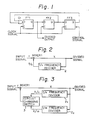
- FIG. 1 shows a typical prior art frequency dividing apparatus comprised of flip-flops FF1, FF2, FF3, and a gate circuit G1.
- the flip-flops FF1, FF2, FF3 are D-type flip-flops having an input D, input C, and output Q (only FF3 has an input M), and the gate circuit G1 is an OR-gate.
- Each of the flip-flops FF1, FF2, FF3 is a 1/2 frequency divider, and the output Q of the flip-flop FF1 is connected to the input D of the flip-flop FF2, the output Q of the flip-flop FF2 is connected to the input D of the flip-flop FF3 and one input of the OR gate G1, and the output Q of the flip-flop FF3 is connected to the other input of OR gate G1.
- the outputs Q of the flip-flops FF2, FF3 are fedback to the input D of the flip-flop FF1 through the OR gate G1.
- the inputs C of the flip-flops FF1, FF2, FF3 are used as common clock signal to be divided, and the inputs D are used for data or as delay signals.
- the input M of the flip-flop FF3 is used as a control signal and an output divided from the output Q of the flip-flop FF1 is made 1/4 or 1/5 by the control signal.
- a 1/4 divided output frequency or a 1/5 divided output frequency can be selected by halting the operation of the flip-flop FF1 intermittently, by controlling the timing of a signal input to the input M of the flip-flop FF3. That is, when the flip-flop FF1 is reset to stop the dividing operation, at a suitable timing obtained by counting the number of clocks, the clock frequency is divided into 1/5 and appears as a divided output of the flip-flop FF1, and when the flip-flop FF1 is activated to start the dividing operation, the clock frequency is divided into 1/4 and appears as a divided output of the flip-flop FF1.
- the clock signal input in the flip-flop FF1 is returned through the flip-flop FF2, FF3 and the gate G1 with a certain delay time, which depends upon the number of gates the signal must pass through, thereby limiting the speed at which the frequency is divided in the dividing apparatus. In other words, when the dividing speed of the dividing apparatus is low, the dividing apparatus can not divide high frequencies.
- the object of the present invention is to provide a frequency dividng apparatus for a high frequency which can divide the frequencies in the microwave band.
- the frequency dividing apparatus is composed of a divider having a fixed dividing ratio, and a mixer for analogically mixing input signals, so that a frequency dividing apparatus able to divide higher frequencies than can be divided by the frequency divider of the prior art conmposed of logical circuits, is realized.
- the presetnt invention provides a frequency dividing apparatus having at least two dividers each having a different fixed dividing ratio, a mixer for analogically mixing input signals, and a circuit changing switch for selecting the divider required, and thus realizes a more reliable variable frequency divider than the variable frequency dividing apparatus of the prior art, in which the output is varied by adjusting the timing of the counting action.
- FIG. 2 is a block diagram showing a first embodiment of a frequency dividing apparatus for high frequencies according to the present invention.
- This frequency dividing apparatus is provided with a mixer 1 and a frequency divider 2.
- the mixer 1 has two input terminals for mixing and one output terminal, and an input terminal of the frequency divider 2 is connected to the output terminal of the mixer 1 and an output terminal of the frequency divider 2 is connected to one input terminal of the mixer 1. An input signal is applied to the other input terminal of the mixer 1.
- Equation (2-1) can be modified as follows.
- the frequency dividing apparatus as shown in Fig. 2 operates as a fractional divider.
- the output signal of the mixer 1 includes frequencies of (f+x/n), x/n, and f other than the frequency of (f-x/n)
- the frequencies x/n and f can be excluded by adopting an balance-type mixer, and the frequency of f+x/n can be excluded by installing a filter or the like in the mixer 1.
- FIG. 3 is a block diagram showing a second embodiment of a frequency dividing apparatus for high frequencies, the output frequency of which is variable, according to the present invention.
- This frequency dividing apparatus is provided with the mixer 1, two frequency dividers 21 and 22 having different dividing ratios, and a circuit changing switch 3.
- the input terminals of the frequency dividers 21 and 22 are connected to one output terminal of the mixer 1, and the output terminals thereof are connected to each input terminal of the circuit changing switch 3.
- An output terminal of the circuit changing switch 3 is connected to the other of the input terminal of the mixer 1.
- the frequency dividing apparatus in Fig. 3 is a basic construction of a variable frequency dividing apparatus for high frequencies.
- the circuit changing switch can be provided with more input terminals, and the frequency dividers connected thereto, to provide a frequency dividing apparatus which can produce three or more divided frequencies.
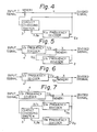
- Figure 4 is a block diagram showing a modification of the second embodiment as shown in Fig. 3.
- the dividing ratio of the frequency divider 21 is set to 1 instead of 1/n, i.e. the frequency divider 21 is replaced by a conductive circuit.
- the divided frequency of 1/2 or m/(m+1) is obtained by switching the circuit changing switch 3.
- FIG. 5 is a block diagram showing a third embodiment of a frequency dividing apparatus according to the present invention.
- a pre-frequency divider 4 is added at a front stage of the frequency dividing apparatus as shown in Fig. 2, and the input signal is applied to the pre-frequency divider 4 and the output signal of the pre-frequency divider 4 is applied to the mixer 3 of the frequency divider shown in Fig. 2.
- Equation (5-1) can be modified as follows. Therefore, the frequency dividing apparatus as shown in Fig. 2 also operates as a fractional divider. Note, if the dividing ratio 1/p of the pre-frequency-divider 4 is equal to the dividing ratio 1/n of the frequency divider 2, the divided frequency x will be 1/(n+1). Namely, the input frequency to the frequency dividing apparatus as shown in Fig. 5 is divided by an integral number.
- Figure 6 is a block diagram showing a modification of the third embodiment as shown in Fig. 5.
- the dividing ratio of the frequency divider 2 is set to 1 instead of 1/n, i.e., the frequency divider 2 is replaced by a conductive circuit.
- the divided frequency of f/2P is obtained.
- FIG. 7 is a block diagram showing a fourth embodiment of the frequency divider according to the present invention.
- a pre-frequency divider 4 is added at a front stage of the frequency dividing apparatus as shown in Fig. 3, and thus the input signal applied to the pre-frequency divider 4 is divided before it is applied to the mixer 1.
- an input frequency is f
- an output frequency is x
- the dividing ratios of the frequency dividers 21 and 22 are 1/n and 1/m
- a dividing ratio of the pre-frequency divider 4 is 1/P
- the divided frequency of fn/p(n+1) or fm/p(m+1) is obtained by switching the circuit changing switch 3, as explained in Fig. 3.
- Figure 8 is a block diagram showing a modification of the fourth embodiment as shown in Fig. 6.
- the dividing ratio of the frequency divider 21 is set to 1 instead of 1/n, i.e., the frequency divider 21 is replaced by a conductive circuit.
- the divided frequency of f/2P or fm/p(m+1) is obtained by switching the circuit changing switch 3.
- Figure 9 is a a concrete embodiment of the frequency dividing apparatus as shown in Fig. 8, which can be realized as an IC (Integrated circuit) by forming a MESFET (Metal Electrode Semiconductor Field Effect Transistor) on a substrate made of GaAs (Gallium arsenide).
- MESFET Metal Electrode Semiconductor Field Effect Transistor
- reference numeral 11 designates a dynamic-type frequency divider (shown in Japanese Patent Application No.
- reference numeral 12 designates a mixer composed of flip-flops
- reference numerals 13, 14 designate differential amplifiers which compensate the mixing loss at the mixer 12 (the amplifier 14 is called a buffer)
- reference numeral 15 designates a circuit changing switch
- reference numeral 16 designates a static-type frequency divider usually composed of flip-flops and operating as a 1/2 frequency divider.
- Figure 10 is a example of a circuit constitution of a dynamic-type frequency divider 11 of Fig.9.
- reference numerals 21, 22 designate differential amplifier and reference numerals 23 to 26 designate switches composed of FET's.
- a normal output terminal of the differential amplifier 21 is connected to an inverted input terminal (-) of the differential amplifier 22 via the FET switch 23, and an inverted output terminal of the differential amplifier 21 is connected to a normal input terminal (+) of the differential amplifier 22 via the FET switch 24, to invert the phase of the output signal of the differential amplifier 22.
- a normal output terminal of the differential amplifier 22 is fedback to a normal input terminal (+) of the differential amplifier 21 via the FET switch 25 and an inverted output terminal of the differential amplifier 22 is fedback to an inverted input terminal (-) of the differential amplifier 21 via the FET switch 26.
- a normal output terminal Q and an inverted output terminal QB of the dynamic-type frequency divider 11 are connected to the input terminals of the differential amplifier 22.
- the FET switches 23 to 26 are turned ON (made conductive) when a high level input signal is applied to each gate.
- a 1/2 frequency of the input signal C can be obtained as an output signal at the output terminals Q and QB when pairs of FET switches 23 and 24, and 25 and 26, are alternately turned ON by the input signal C.
- Figure 11 is a known example of a circuit constitution of the differential amplifier as shown in Fig. 10.
- the differential amplifier in Fig.11 is composed of seven FET's 28 to 30 and 37 to 39, series-connected diodes D1,D2 for shifting the level of the output voltage, a diode D2, and two resistors R1,R2.
- a normal input terminal IN is connected to a gate of the FET 27 and an inverted input terminal INB is connected to a gate of the FET 28, and a normal output terminal OUT is connected to a cathode of the series-connected diode D2 and an inverted output terminal OUTB is connected to a cathode of series-connected diode D1.
- Figure 12 is a example of a circuit constitution of the mixer 12 of Fig.9.
- reference numerals 31, 32, 34,and 35 designate AND gates
- reference numerals 33 and 36 designate NOR gates
- references LOCAL, LOCALB, SIGNAL, and SIGNALB designate input signals to the mixture 12.
- the input signals LOCAL, LOCALB, SIGNAL, and SIGNALB are a normal signal and an inverted output signal of the dynamic-type frequency divider, and a normal output and an inverted output of the circuit changing switch, respectively.
- a logical product of the signals LOCAL and SIGNAL is obtained by the AND gate 31, a logical product of the signals LOCALB and SIGNALB is obtained by the AND gate 32, a logical product of the signals LOCALB and SIGNAL is obtained by the AND gate 34, and a logical product of the signals LOCAL and SIGNALB is obtained by the AND gate 32.
- the NOR gate 33 then logically adds the output signals of the AND gates 31 and 32 and outputs the added signal after inverting same, and the NOR gate 36 also logically adds the output signals of the AND gates 34 and 35 and outputs the added signal after inverting same.
- the logical circuit in Fig. 12 is constructed as a exclusive OR circuit, and thus is made to operate as a mixer by the multiplicative action of the exclusive OR circuit.
- Figure 13 is a example of a circuit constitution of the circuit changing switch 15 of Fig.9.
- reference numerals 41, 42, 44, and 45 designate AND gates
- reference numerals 43 and 46 designate NOR gates
- references Da, Db, DaB, and DbB designate data signals
- references M and MB designate control signals.
- the data signals Da, Db, DaB, and DbB are input to one input terminal of the AND gates 41, 42, 44, and 45 respectively
- the control signal M is input to the other input terminal of the AND gates 41 and 44
- the control signal MB is input to the other input terminal of the AND gates 42 and 45.
- the output signals of the AND gates 41 and 42 are input to the NOR gate 43, and the output signals of the AND gates 44 and 45 are input to the NOR gate 46, and as a result, when the control signal M is high level and the control signal MB is low level, the data signals Da and DaB appear at the outputs of the NOR gates 46 and 43, respectively, and when the control signal M is low level and the control signal MB is high level, the data signals Db and DbB appear at the outputs of the NOR gates 46 and 43, respectively. Accordingly, the logical circuit in Fig. 13 operates as a circuit changing switch.
- FIG 14 is a circuit diagram of the constitution of the static-type frequency divider 16 of Fig. 9.
- the static-type frequency divider 16 is composed of two RS flip-flops 51 and 52, each of which is constructed by a pair of logical circuits composed of two AND gates and a NAND gate.
- An input S of the flip-flop 51 is connected to a normal output Q of the flip-flop 52
- an input R of the flip-flop 51 is connected to an inverted output QB of the flip-flop 52
- an input S of the flip-flop 52 is connected to an inverted output QB of the flip-flop 51
- an input R of the flip-flop 52 is connected to a normal output Q of the flip-flop 52.
- signals C and CB are input to each logical circuit.
- the output of the flip-flops 51 and 52 are inverted alternately by the input of the control signals C and CB, and thus the frequencies of the signals C and CB are divided into 1/2 and appear at the outputs Q and QB of the flip-flop 52.
- FIG. 15 is a circuit diagram showing the constitution of the flip-flop shown in Fig. 14.
- the flip-flop in Fig. 15 is composed of three differential amplifiers each of which comprises a pair of FET's 53 and 54, 55 and 56, and 57 and 58.
- the source of the FET's 53 and 56, the phases of which are different, and the drain of the FET 57 are connected together, and the source of the FET's 54 and 55, the phases of which are different, and the drain of the FET 58 are connected together.
- the drain of FET's 53 and 54 and the drain of FET's 55 and 56 are connected together, and each of the connecting points is connected respectively to the gates of the FET's 59 and 60, which constitute a source follower.
- the input R is connected to the gate of the FET 53
- the input S is connected to the gate of the FET 56
- the output Q is connected to the connecting point of the source of the FET 60 and the gate of the FET 54
- the output QB is connected to the connecting point of the source of the FET 59 and the gate of FET 55.
- the signals C and CB are input to the bases of the FET's 57 and 58, respectively, and the output signals Q and QB are inverted at every input of the signals C and CB, and thus the flip-flop circuit operates as a master-slave type flip-flop.
- Figure 16 shows wave forms for explaining the operation of the frequency dividing apparatus as shown in Fig. 8. These wave forms are obtained by a simulation, wherein each gate is made of Au/WSi and each gate length is 1 ⁇ m. In this simulation, a frequency of 7 GHz is input as an input signal, and the dividing ratio of the frequency divider 2 and the pre-frequency divider 4 are both set to 1/2, so that a 7/3 GHz or 7/4 GHz divided frequency is obtained as an output signal.
- the wave form f indicates an input frequency
- the wave form x indicates an output frequency
- the wave form y indicates a signal input to the circuit changing switch 15.
- the time t3 indicates the switching of the circuit changing switch 15, and the feedback frequency from the amplifier 13 is directly applied to the mixer 12 before the time t3 where the total dividing ratio of the input frequency is 1/4, and then the frequency fedback from the amplifier 13 is applied via the static-type frequency divider 16, where the total dividing ratio of the input frequency is 1/3.
- the input frequency f has four cycles and one frequency is output
- the input frequency f has three cycles and one frequency is output. Accordingly, it can be understood that the divided frequency of f/3 or f/4 is obtained by switching the circuit changing switch 3.
- Au/WSi gate is explained in: [Au/TiN/WSi-Gate Seef-Aligned GaAs MESFETs Using Rapid Terminal Annealing Method ] Electronics Letters 1985, Vol. 21 No. 18 p804, by Shigaki et al.
- a dynamic-type frequency divider having a fixed frequency dividing ratio can be used as shown in Fig. 9, or a static-type frequency divider having a fixed frequency dividing ratio, or an analog-type frequency dividing apparatus having a variable frequency dividing ratio as shown in Fig. 7 of the present invention, can be used.
Landscapes
- Stabilization Of Oscillater, Synchronisation, Frequency Synthesizers (AREA)
- Superheterodyne Receivers (AREA)
Applications Claiming Priority (2)
| Application Number | Priority Date | Filing Date | Title |
|---|---|---|---|
| JP62125578A JPS63290408A (ja) | 1987-05-22 | 1987-05-22 | 高速可変分周器 |
| JP125578/87 | 1987-05-22 |
Publications (2)
| Publication Number | Publication Date |
|---|---|
| EP0292002A2 true EP0292002A2 (fr) | 1988-11-23 |
| EP0292002A3 EP0292002A3 (fr) | 1990-12-19 |
Family
ID=14913651
Family Applications (1)
| Application Number | Title | Priority Date | Filing Date |
|---|---|---|---|
| EP19880108129 Withdrawn EP0292002A3 (fr) | 1987-05-22 | 1988-05-20 | Diviseur de fréquence pour fréquence élevée |
Country Status (3)
| Country | Link |
|---|---|
| US (1) | US4855895A (fr) |
| EP (1) | EP0292002A3 (fr) |
| JP (1) | JPS63290408A (fr) |
Cited By (1)
| Publication number | Priority date | Publication date | Assignee | Title |
|---|---|---|---|---|
| FR2828599A1 (fr) * | 2001-08-13 | 2003-02-14 | Stepmind | Circuit melangeur a rejection de frequence image, notamment pour un recepteur rf a frequence intermediaire nulle ou faible |
Families Citing this family (7)
| Publication number | Priority date | Publication date | Assignee | Title |
|---|---|---|---|---|
| JPH06104289A (ja) * | 1992-09-18 | 1994-04-15 | Hitachi Ltd | 半導体装置およびそれを用いた増幅回路 |
| JPH0738423A (ja) * | 1993-07-23 | 1995-02-07 | Mitsubishi Electric Corp | 分周回路 |
| US7164122B2 (en) * | 2000-02-29 | 2007-01-16 | Ionwerks, Inc. | Ion mobility spectrometer |
| JP3990123B2 (ja) * | 2001-07-17 | 2007-10-10 | 日本電気株式会社 | サンプラーおよび計測方法 |
| US20050104634A1 (en) * | 2003-11-19 | 2005-05-19 | Minoru Fujishima | Frequency divider, PLL circuit and semiconductor integrated circuit |
| US7564276B2 (en) * | 2006-06-28 | 2009-07-21 | Qualcomm Incorporated | Low-power modulus divider stage |
| US7952399B1 (en) * | 2009-01-19 | 2011-05-31 | Lockheed Martin Corporation | Low phase noise high speed digital divider |
Family Cites Families (7)
| Publication number | Priority date | Publication date | Assignee | Title |
|---|---|---|---|---|
| CA611727A (en) * | 1961-01-03 | Western Electric Company, Incorporated | Frequency divider circuits | |
| JPS60172807A (ja) * | 1984-02-13 | 1985-09-06 | Nippon Telegr & Teleph Corp <Ntt> | 分周回路 |
| JPS60172808A (ja) * | 1984-02-13 | 1985-09-06 | Nippon Telegr & Teleph Corp <Ntt> | 分周回路 |
| US4638180A (en) * | 1984-03-09 | 1987-01-20 | Matsushita Electric Industrial Co., Ltd. | Frequency divider circuits |
| US4631500A (en) * | 1984-04-24 | 1986-12-23 | The United States Of America As Represented By The Secretary Of The Navy | Microwave frequency divider having regenerative oscillation |
| DE3579365D1 (de) * | 1984-05-16 | 1990-10-04 | Siemens Ag | Breitbandfrequenzteiler. |
| DE3509327A1 (de) * | 1985-03-15 | 1986-09-25 | Telefunken electronic GmbH, 7100 Heilbronn | Dynamischer frequenzteiler mit mischstufe und verstaerker |
-
1987
- 1987-05-22 JP JP62125578A patent/JPS63290408A/ja active Pending
-
1988
- 1988-05-19 US US07/196,620 patent/US4855895A/en not_active Expired - Fee Related
- 1988-05-20 EP EP19880108129 patent/EP0292002A3/fr not_active Withdrawn
Cited By (4)
| Publication number | Priority date | Publication date | Assignee | Title |
|---|---|---|---|---|
| FR2828599A1 (fr) * | 2001-08-13 | 2003-02-14 | Stepmind | Circuit melangeur a rejection de frequence image, notamment pour un recepteur rf a frequence intermediaire nulle ou faible |
| WO2003017465A1 (fr) * | 2001-08-13 | 2003-02-27 | Stepmind | Circuit melangeur a rejection de frequence image, notamment pour un recepteur rf a frequence intermediaire nulle ou faible |
| US7043221B2 (en) | 2001-08-13 | 2006-05-09 | Stepmind | Mixer circuit with image frequency rejection, in particular for an RF receiver with zero or low intermediate frequency |
| CN100448164C (zh) * | 2001-08-13 | 2008-12-31 | 斯德普曼德公司 | 具有镜频抑制的混合器电路,尤其对于零或低中频的射频接收机 |
Also Published As
| Publication number | Publication date |
|---|---|
| US4855895A (en) | 1989-08-08 |
| JPS63290408A (ja) | 1988-11-28 |
| EP0292002A3 (fr) | 1990-12-19 |
Similar Documents
| Publication | Publication Date | Title |
|---|---|---|
| US4951303A (en) | High speed digital programmable frequency divider | |
| US6970025B2 (en) | Programmable frequency divider | |
| US6194947B1 (en) | VCO-mixer structure | |
| US5004933A (en) | Phase-selectable flip-flop | |
| EP0973262B1 (fr) | Circuit logique fonctionnant en mode de commutation de courant | |
| EP0276130A2 (fr) | Circuits mélangeurs de signaux électriques | |
| KR830004002A (ko) | Fsk신호용 무선수신기 | |
| EP0292002A2 (fr) | Diviseur de fréquence pour fréquence élevée | |
| US6154077A (en) | Bistable flip-flop | |
| US6282255B1 (en) | Frequency divider with variable modulo | |
| EP1020031B1 (fr) | Circuit integre | |
| JPS59168706A (ja) | アナログ型非同調1/2分周回路 | |
| US5086441A (en) | Frequency divider circuit | |
| EP0020778A1 (fr) | Circuit amplificateur | |
| JPH0430762B2 (fr) | ||
| KR940009333B1 (ko) | 집적 전자 다중 회로 | |
| KR100273862B1 (ko) | 이중수퍼헤테로다인형수신회로 | |
| US5557649A (en) | Circuit configuration for dividing a clock signal | |
| KR20010053564A (ko) | 텔레커뮤니케이션 ic용 다중 주파수 저전력 발진기 | |
| EP0899878A1 (fr) | Bascube bistable à surface d'intégration réduite | |
| JPH0352041Y2 (fr) | ||
| JP3429657B2 (ja) | 分周器 | |
| JPH0326929B2 (fr) | ||
| GB1231350A (fr) | ||
| JP2985483B2 (ja) | モノリシック半導体集積回路化した周波数分周器 |
Legal Events
| Date | Code | Title | Description |
|---|---|---|---|
| PUAI | Public reference made under article 153(3) epc to a published international application that has entered the european phase |
Free format text: ORIGINAL CODE: 0009012 |
|
| AK | Designated contracting states |
Kind code of ref document: A2 Designated state(s): DE FR GB IT |
|
| PUAL | Search report despatched |
Free format text: ORIGINAL CODE: 0009013 |
|
| AK | Designated contracting states |
Kind code of ref document: A3 Designated state(s): DE FR GB IT |
|
| 17P | Request for examination filed |
Effective date: 19901220 |
|
| 17Q | First examination report despatched |
Effective date: 19921020 |
|
| STAA | Information on the status of an ep patent application or granted ep patent |
Free format text: STATUS: THE APPLICATION HAS BEEN WITHDRAWN |
|
| 18W | Application withdrawn |
Withdrawal date: 19950713 |
|
| R18W | Application withdrawn (corrected) |
Effective date: 19950713 |