EP0295683A2 - Schutzschaltung für eine Batteriespeiseschaltung - Google Patents
Schutzschaltung für eine Batteriespeiseschaltung Download PDFInfo
- Publication number
- EP0295683A2 EP0295683A2 EP88109654A EP88109654A EP0295683A2 EP 0295683 A2 EP0295683 A2 EP 0295683A2 EP 88109654 A EP88109654 A EP 88109654A EP 88109654 A EP88109654 A EP 88109654A EP 0295683 A2 EP0295683 A2 EP 0295683A2
- Authority
- EP
- European Patent Office
- Prior art keywords
- circuit
- transistor
- battery feed
- voltage
- current
- Prior art date
- Legal status (The legal status is an assumption and is not a legal conclusion. Google has not performed a legal analysis and makes no representation as to the accuracy of the status listed.)
- Granted
Links
Images


Classifications
-
- H—ELECTRICITY
- H04—ELECTRIC COMMUNICATION TECHNIQUE
- H04M—TELEPHONIC COMMUNICATION
- H04M3/00—Automatic or semi-automatic exchanges
- H04M3/18—Automatic or semi-automatic exchanges with means for reducing interference or noise; with means for reducing effects due to line faults with means for protecting lines
-
- H—ELECTRICITY
- H02—GENERATION; CONVERSION OR DISTRIBUTION OF ELECTRIC POWER
- H02H—EMERGENCY PROTECTIVE CIRCUIT ARRANGEMENTS
- H02H9/00—Emergency protective circuit arrangements for limiting excess current or voltage without disconnection
- H02H9/02—Emergency protective circuit arrangements for limiting excess current or voltage without disconnection responsive to excess current
- H02H9/025—Current limitation using field effect transistors
-
- H—ELECTRICITY
- H04—ELECTRIC COMMUNICATION TECHNIQUE
- H04M—TELEPHONIC COMMUNICATION
- H04M19/00—Current supply arrangements for telephone systems
- H04M19/001—Current supply source at the exchanger providing current to substations
Definitions
- the present invention relates to a switching system, more specifically it relates to a protection circuit for protecting a battery feed circuit in a line circuit from a ground fault and a false connection.
- a protection circuit is fitted to the battery feed circuit to protect the same when a ground fault or false connection occurs, by limiting the amount of overcurrent flowing therethrough.
- a prior art protection circuit is realized by inserting a well known limiting resistor between the subscriber's line and the battery feed circuit, only when a fault such as ground fault or false connection is detected, and another prior art protection circuit is realized by a plurality of auxiliary power transistors, connected in parallel with a main battery feed transistor, to cope with an overcurrent.
- an object of the present invention is to provide a protection circuit for a battery feed circuit, which protection circuit can be minituarized in the form of an integrated circuit (IC).
- IC integrated circuit
- the protection circuit according to the present invention is realized by a voltage limiting circuit which limits the voltage across a battery feed resistor to a predetermined value when a fault is detected.
- FIG. 1 is a block diagram of a protection circuit according to a first embodiment of the present invention.
- R 1 denotes a battery feed resistor for determining a DC current supplied to the subscriber's line.
- the resistor R 1 is connected to a power source (not shown) via a battery feed transistor Q 1 .
- the base of the transistor Q 1 is connected to the output of an operational amplifier OP 1 , one of the inputs of which is connected to an intermediate connecting point between resistors R 2 and R 3 for determining an AC impedance of the battery feed circuit.
- a voltage limiting circuit 12′ for the resistor R 1 is employed, which is controlled by a supervising circuit 11. Namely, if a fault occurs and an overcurrent is generated, the overcurrent is detected at the resistor R 1 by the supervising circuit 11, and the circuit 11 commands the circuit 12′ to clamp the voltage across the resistor R 1 at a predetermined voltage.
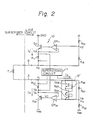
- FIG. 2 is a detailed circuit diagram of the first embodiment shown in Fig. 1.
- Fig. 2 only a protection circuit for a protection against a ground fault is illustrated for brevity, but a protection circuit for protection against a false connection also can be mounted.
- a battery feed circuit 10 is illustrated, which is mounted in a corresponding line circuit for a related telephone terminal equipment T connected via the subscriber's lines, i.e., the A line and the B line.
- the battery feed circuit 10 has a symmetric construction with respect to the A and B lines, and therefore, the following explanation will be made with reference mainly to the circuit part of the A line, i.e., the bottom half portion of the Figure.
- Resistors R 12 and R 13 (B line side) comprising a voltage divider are connected between a ground GND and the B line.
- resistors R 22 and R 23 are connected between a power source V BB , e.g., -48 V, and the A line.
- V BB power source
- a DC current flows from the ground GND to the power source V BB via the resistors R 12 and R 13 , the telephone terminal T, and the resistors R 23 and R 22 . Accordingly, a voltage V B appears at the intermediate connecting point between the resistors R 23 and R 22 .
- the battery feed transistor Q 21 is connected, via the battery feed resistor R 21 , between the A line and the power source V BB .
- the connection point V B is connected to a noninverting input terminal (+) of the operational amplifier OP 21 , the inverting input terminal (-) of which is connected to the emitter of the battery feed transistor Q 21 and the base of which is connected to the output of the amplifier Q 21 .
- the DC resistance value, at the B line side, of the battery feed circuit 10 is made equal to the constant value of the A line side by a suitable circuit arrangement.
- the DC resistance values of the A and B line sides are usually made equal and selected to be a relatively low value, such as about 200 ⁇ .
- the AC voltage across the A and B lines is divided by the resistors R22 and R23 and produces a voltage V b at the intermediate connecting point therebetween.
- the voltage V b induces an AC voltage V b at the inverting input (-) of the operational amplifier OP21.
- the AC voltage on the B line is divided by the resistors R12 and R13 to produce a voltage V b ′.
- the voltage V b ′ is applied to the non inverting input (+) of an operational amplifier OP11 to produce an identical AC voltage V b ′ at the inverting input (-) thereof.
- the AC voltages appearing at the emitters of the battery feed transistors Q21 and Q11 are identical to those appearing on the A and B lines, respectively, and thus an AC current (speech current) does not flow through the transistors Q21 and Q11. Therefore, the respective AC impedances are defined by the resistors R22 and R23 (A line side) and the resistors R12 and R13 (B line side), respectively, to obtain a relatively high constant value, such as several tens of k ⁇ .
- the voltage limiting circuit 12′ is comprised of three transistors connected in series, each having the same conductivity type (a PNP type is used in Fig. 2).
- the first transistor is a saturation transistor having a resistor between the base and the emitter thereof, the base receiving a first control signal, i.e., a detection current I0.
- the second and third transistors are each connected in the form of a diode. If a ground fault does not occur at the A line, a detection current I0 , i.e., a first control signal, is not provided from the supervising circuit 11.
- the voltage limiting circuit 12′ a current does not flow through the transistor Q22 , but if a ground fault does occur at the A line side, the current I A is increased.
- the current I A is equal to V BB /2 x R21 and larger than a rated current value.
- the transistor Q21 and the resistor R21 may be damaged by burning. In the circuit of Fig. 2, this possibility is eliminated because the voltage limiting circuit 12′ is employed.
- the voltage limiting circuit 12′ is directly incorporated into a portion at which the high impedance against the AC voltage is created. Accordingly, during protection against the ground fault, the voltage across the resistor R23 is limited by the circuit 12′, and therefore, the AC impedances at the A and B lines are unbalanced. This condition is worsened because the unbalance impedances induce an oscillation inside the battery feed circuit 10, and this undesired oscillation current is superimposed onto the DC current I A .
- the protection circuit according to the present invention eliminates the above-mentioned problem of undesired oscillation.
- FIG. 3 is a block diagram of a protection circuit according to a second embodiment of the present invention.
- the protection circuit of the second embodiment is comprised of the aforesaid supervising circuit 11, a voltage limiting circuit 12 which is slightly different from the aforesaid circuit 12′, and an operational amplifier control circuit 13.
- the supervising circuit 11 detects the voltage across the battery feed resistor R1 to produce a first control signal and a second control signal, I0 and I S , respectively.
- the voltage limiting circuit 12 is connected between both ends of the battery feed resistor R1 to limit the voltage across the battery feed resistor R1 in accordance with the first control signal I0 (detection current), and the operational amplifier control circuit 13 stops the operation of the amplifier OP1 in accordance with the second control signal I S , i.e., a stop control current.
- the voltage limiting circuit 12 is not directly connected with the resistors R2 and R3 , both defining the aforesaid AC impedance, and accordingly, the AC impedance is not varied by the addition of the circuit 12. Therefore, an imbalance in the AC impedance between the A and B lines is not created, and thus a deleterious oscillation is not generated in the battery feed circuit.
- Figure 4 is a detailed circuit diagram of the second embodiment shown in Fig. 3. It should be understood that the protection circuit of Fig. 4 is designed to cope with, for example, a ground fault, and members identical to those explained before are given the same reference numerals or symbols (as for all later figures).
- the voltage limiting circuit 12 is comprised of a first saturation transistor receiving, at the base thereof, the first control signal I0 , a second transistor connected in the form of a diode, both of which have the same conductivity type and are connected in series, and a third transistor having another conductivity type, the base of which is connected with the emitter of the battery feed transistor, and these three series-connected transistors are connected between the subscriber's line and the base of the battery feed transistor.
- the voltage limiting circuit 12 is comprised of transistors Q25 and Q26 , both of which are NPN type, a PNP type transistor Q27 , and resistors R25 and R27.
- the transistors Q25 through Q27 are inserted between the A line and the base of the battery feed transistor Q21 , and the transistor Q26 is connected in the form of a diode. Further, the base of the transistor Q27 is connected to the emitter of the transistor Q21.
- the operational amplifier control circuit 13 is connected between the supervising circuit 11 and the operational amplifier OP21.
- the operation of the battery feed circuit 10 shown in Fig. 4 is substantially the same as that of the corresponding circuit shown in Fig. 2.
- the supervising circuit 11 does not provides a current I0 , and accordingly, a current does not flow through the transistor Q25 , and thus there is no operational change in the battery feed circuit 10.
- the battery feed current I A is increased, and the related increase is detected as an increased voltage across the battery feed resistor R21 which then produces the current I0. Accordingly, the transistor Q25 is saturated and the interval resistance value thereof is reduced. Therefore, the voltage V A at the battery feed resistor R21 is limited to the sum of the base-emitter voltages V BE26 and V BE27 of the corresponding transistors Q26 and Q27.
- the ground fault current I G equals V BB /2xR21 , which is larger than the rated current value.
- the output current of the operational amplifier OP21 is very large, and therefore, the base current I BE21 of the transistor Q21 and the current flowing through the transistors Q25 through Q27 become large.
- the supervising circuit 11 produces a second control signal, i.e., a stop control current I S , and supplies that signal to an operational amplifier control circuit 13. Accordingly, the circuit 13 makes a current source OFF, which current source supplies power to the operational amplifier OP21 , and thus, during the protection against a ground fault, the operation of the operational amplifier OP21 is stopped.
- the currents I B21 and I Q are made small and the ground fault current I G is limited by the transistors Q25 through Q27 to the current I0 flowing through the resistor R25.
- the resistor R27 (as for a resistor R17 in Fig. 5) maintains the battery feed transistor Q21 in an active state, and the base current of Q21 flows through resistor R27.
- the resistor R27 acts as a hold resistor for holding the transistor Q27 in an active state.
- Figure 5 is a circuit diagram of an example of an application of the second embodiment of the present invention.
- the protection circuit can cope with not only a ground fault on the A line, but also with a false connection of the B line to the power source V BB , e.g., -48 V.
- reference numeral 12-1 is a voltage limiting circuit which contains transistors Q15 , Q16 , and Q17 and resistors R15 and R17
- reference numeral 13-1 represents an operational amplifier control circuit.
- Fig. 5 the construction and the operation of the battery feed circuit 10 for the A and B lines are substantially the same as those explained before with reference to Figs. 2 and 4. Also, the construction and the operation of the voltage limiting circuit 12-2, containing the transistors Q25 , Q26 , Q27 and the resistors R25 and R27 , and the control circuit 13-2, are identical to those explained before with reference to Fig. 4.
- the voltage limiting circuit 12-1 comprised of the transistors Q15 , Q16 , Q17 and the resistors R15 and R18 is used for protection against an overcurrent produced when a false connection occurs.
- the transistors Q15 through Q17 are connected between the B line and the base of the transistor Q11 , the transistor Q16 is connected in the form of a diode, and the transistor Q17 is connected, at the base thereof, with the emitter of the battery feed transistor Q11.
- a false connection current I C is expressed as follows.
- the current I C is reduced to the above defined value, and thus the purpose of the present invention is realized.
- the supervising circuit 11 must also supply a second control signal, i.e., a stop control current I S1 , to the control circuit 13-1, at the same time as the detection current I01 is absorbed by the circuit 11, so that the circuit 13-1 makes a current source OFF, which current source supplies power to the operational amplifier OP11 , and thus, the operation of the amplifier OP11 is stopped.
- a second control signal i.e., a stop control current I S1
- Figure 6 is a circuit diagram of an example of the supervising circuit.
- Reference characters R11 and R21 denote the aforesaid battery feed resistors
- Q31 through Q39 are transistors
- R33 , R34 and R35 are resistors
- M a1 , M a2 , M a3 and M b1 , M b2 and M b3 are current mirror circuits.
- This current flows via the transistor Q35 and creates a voltage drop across the resistor R35 , and this voltage drop is composed with a threshold voltage V th at a comparator comprised of the transistors Q38 and Q39.
- V th a threshold voltage
- a signal is output to the mirror circuit M a3 to make the M a3 ON and thus output the detection current I02.
- the current I02 is supplied, as explained with reference to Figs. 4 and 5, to the voltage limiting circuit 12 upon the detection of a ground fault.
- the ON-OFF control of the operational amplifiers OP21 and OP11 can be effected by the second control signals, i.e., the stop control currents, which can be produced in the same manner as the aforesaid currents I01 and I02 , which stop control currents are output to the respective control circuits 13-1 and 13-2, which make the corresponding current sources OFF to stop the operation of the operational amplifiers.
- the second control signals i.e., the stop control currents
- FIG. 7 is a circuit diagram of another type of battery feed circuit.
- the battery feed circuit is equipped with resistors R41 , R42 , R43 , and R44 and a capacitor C0.
- the battery feed circuit of Fig. 7 contains the protection circuit shown in Fig. 2.
- the supervising circuit 11 issues an indication to an operator that a short-circuit exists in the battery feed circuit. According to the indication, the operator starts the restoration of the circuit from a ground fault or a false connection condition. Note, the restoration per se is not the object of the present invention.
- the operational amplifier control circuit 13 of Fig. 4 (same as the circuits 13-1 and 13-2 of Fig. 5). Namely, in one method, they connected a limiting resistor in series with the output of the operational amplifier, and in the other method, they cut off the power source (V CC , V BB ) for the operational amplifier; i.e., when the operational amplifier is to be stopped, the power source is cut off.
- the first method had a defect in that the limiting resistor was not suitable for practical use; since such a limiting resistor must have a considerably high resistance, and such a high resistance value element is not easily fabricated in a large scale integration circuit (LSI).
- LSI large scale integration circuit
- the second method had a defect in that the manufacturing process became complicated, since first a relatively wide power line must be partially removed and then an analog switch must be inserted into the removed part. Further, it is not preferable to cut off the power line, since the thus cut power line is liable to induce noise.
- control circuit 13,13-1,13-2 which can smoothly stop or limit the output current of the operational amplifier and can be constructed with a simple design.
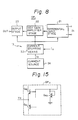
- FIG 8 is a block diagram of a control circuit according to the present invention and an operational amplifier.
- the operational amplifier OP1 (same for OP11 and OP21) includes a differential input stage 21, a high gain amplifier stage 22, an output stage 23, and a current source 24 providing a driving current I D for driving the above-mentioned three stages 21, 22, and 23.
- the driving current I D can be made ON or OFF by a current stopping means 30.
- the current stopping means 30 corresponds to the aforesaid operational amplifier control circuit 13 (13-1,13-2) and receives the second control signal, i.e., the stop control current I S (see I S in Fig. 4, and I S1 I S2 in Fig. 5).
- the operational amplifier OP1 is supplied with a driving current from the current source 24 and then performs the required operational amplifying function. Taking this into consideration, the driving current I D from the current source 24 is stopped to stop the operation of the operational amplifier per se, and thus the current stopping means 30 is incorporated into the well known operational amplifier OP1.
- the operation of the operational amplifier can be smoothly stopped without using the aforesaid limiting resistor at the output of the operational amplifier or inserting the aforesaid analog switch into the power line (V CC , V BB ).
- Figure 9 is a circuit diagram of an operational amplifier incorporating an example of an operational amplifier control circuit according to the present invention.
- a well known differential input stage 21 is comprised of transistors Q46 and Q47
- a well known high gain amplifier stage 22 is comprised of transistors Q42 , Q48 , and Q49
- a well known output stage 23 is comprised of transistors Q40 and Q41.
- a well known current source 24 is provided with a constant current source 24-1, comprised of a current mirror circuit 41, and a current supply element 24-2 connected therewith via a current line L1.
- the supply element 24-2 is provided with a current mirror circuit 42.
- the constant current source 24-1 contains a diode D1 which produces the aforesaid driving current I D having a value which is determined by a division of the forward voltage of the diode D1 by the resistance value of a resistor R50.
- the driving current I D is given to each of the stages (21, 22, 23), via the current supply element 24-2, to drive the same.
- the bypassing means 31 is made conductive by the second control signal, i.e., the stop control current I S , to bypass the current flowing through an input transistor Q51 of the current mirror circuit 41. Accordingly, the driving current I D flowing through an output transistor Q50 is also stopped, and thus the operation of the operational amplifier OP1 is stopped.
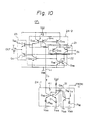
- FIG. 10 is detailed circuit diagram of an operational amplifier and control circuit of Fig. 9.
- the bypassing means 31 of Fig. 9 is specifically realized as a transistor Q52 , to which the stop control current I S is input at the base thereof, to saturate the transistor Q52 , and thus the collector-emitter voltage V CE is reduced, for example, to about 0.1 V through 0.2 V.
- the aforesaid forward voltage, usually about 0.7 V, of the diode D1 is not applied to the resistor R50 , and thus the driving current I D is not generated.
- the operation of the operational amplifier OP1 is stopped by the stop control current I S .
- a commercially available operational amplifier is not equipped with an external terminal suitable for connection with the bypassing means 31 (transistor Q52 and resistor R52), and thus it is advisable to prefabricate the bypassing means 31 during the LSI process of the related circuit.
- the LSI package should be provided with an input terminal (pin) for receiving the current I S .
- Figure 11 is simple circuit diagram representing a battery feed circuit.
- the battery feed circuit 10 is substantially the same as that described previously.
- Figure 12 is a schematic circuit diagram representing the circuit of Fig.11 in which a B line ground fault has occurred.
- the characters Q11 , OP11 , B, T, A, V CC , V BB and GND represent the same elements as in previous Figures.
- the circuit In the battery feed circuit 10, if a B line ground fault occurs, the circuit is in the state shown in Fig. 12.
- the dynamic range in the voltage of the operational amplifier OP11 is smaller than the positive power source voltage to be actually applied to the OP11 , and accordingly, a voltage higher than the ground level is used for the positive power source voltage to obtain an operational margin, which higher voltage is, for example, +5 V, i.e., V CC . Due to the higher voltage V CC , the output voltage of the operational amplifier OP11 becomes higher than the ground level by a base-emitter voltage V BE11 of the transistor Q11 , and accordingly, a positive voltage, sent from the base to the collector of the Q11 , appears.
- the protection circuit for limiting the current through the battery feed transistor Q11 which does not produce the disadvantage mentioned above, will be described below with reference to Figs. 13 and 14.
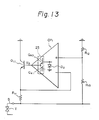
- Figure 13 is a general circuit diagram of a battery feed circuit containing a protection circuit for a B line false connection.
- the clamping means can be specifically realized as a diode (referenced by D2), i.e., a voltage clamping diode.
- D2 referenced by D2
- the transistor Q40 of the output stage 23 (Fig. 9) is grounded, at the base thereof, by the voltage clamping diode for D2.
- a transistor connected in the form of a diode, can be used (described hereinafter), and thus the output voltage of the output stage 23 can be limited to suppress the aforesaid undesired current.
- the voltage, applied to the base of the Q40 can be lower than the voltage across the diode D2 , i.e., the output voltage V0 of the amplifier OP11 is made lower than the voltage across the diode D2 by the base-emitter voltage of the transistor Q40. Therefore, the voltage V0 is limited to the ground level, and the undesired current produced from the transistor Q11 is stopped, even if the B line is erroneously grounded.
- FIG 14 is a detailed circuit diagram of an operational amplifier containing a protection circuit for the B line ground fault.
- the operational amplifier of Fig.14 is slightly different from that disclosed before, but the function thereof is substantially the same as previously described.
- reference numeral 25 represents a bias generating circuit for the output stage 23, which circuit 25 is comprised of transistors Q54 and Q56.
- the base of the transistor Q40 is connected to the ground GND by the voltage clamping diode D2 , to limit the potential at a point "a". Accordingly, the voltage potential at the point "a", relative to the ground GND, is lower by the forward voltage V F .
- this voltage V F is usually about 0.6 V through 0.7 V, when a silicon diode is used.
- the output voltage V0 of the amplifier OP11 can be expressed as follows. V0 ⁇ V a - V BE40 where V BE40 denotes the base-emitter voltage of the transistor Q40 , and V a is a voltage at the point "a". If the value V BE40 is equal to the formed voltage V F , the output voltage V0 of the amplifier OP11 can be made lower than zero volt, by suitably setting the transistor Q40 and the diode D2.
- the output voltage V0 of the amplifier OP11 does not become higher than the ground level, even if a B line ground fault occurs, which prevents the generation of the aforesaid undesired current of the transistor Q11.
- Figure 15 shows another type voltage clamping diode wherein the ground level clamping means is fabricated by a transistor Q60 connected in the form of a diode.
- the transistor Q60 is an NPN type and the emitter thereof is grounded, and the base and the collector thereof are connected to each other.
- the base-emitter voltage is utilized as the clamping voltage, which is usually about 0.6 V through 0.7 V, when silicon is used. If the transistors Q40 and Q60 have the same base-emitter voltage V BE , the output voltage V0 can be set lower than zero volt. Accordingly, a same conductivity type transistor as the transistor Q40 is used, i.e., the NPN transistor Q60. As is well known, transistors of the same conductivity type exhibit almost the same base-emitter voltage, on the same IC chip.
- Figure 16 is a circuit diagram representing a part of the circuit shown in Fig. 5, and all members thereof, except for a detection circuit 51, have been already explained. Note, the detection circuit 51 has also been disclosed as the circuit of Fig. 6, except for the addition of the current mirror circuit M b3 .
- the detection circuit 51 detects the voltage across the battery feed resistor R11 and the first control signal, i.e., the detection current I01 , is output therefrom.
- a current, identical to I01 flows through a transistor Q62 , and through a transistor Q63 , and thus the transistor Q15 is saturated.
- V R V BE16 + V BE17 + V CE15(SAT)
- V BE16 and V BE17 denote the base-emitter voltages of the corresponding transistors Q16 and Q17
- the collector-emitter voltage V CE63 of the transistor Q63 can be fully maintained, so that the mirror circuit M b3 can operate normally.
- the voltage at the point "b" of Fig. 16 becomes substantially equal to the voltage of V BB .
- the collector-emitter voltage V CE63 of the transistor Q63 cannot be fully obtained, and thus the mirror circuit M b3 cannot operate normally. Accordingly, it is not possible to saturate transistor Q15 , and thus the transistor Q15 cannot operate to limit the voltage V R across the battery feed resistor R11. Namely, an overcurrent continues to flow.
- the present inventors further propose a circuit arrangement of the protection circuit which will firmly suppress an overcurrent even if a false connection occurs, which false connection does not include the resistor component (r).
- Figure 17 depicts a circuit arrangement of a protection circuit to cope with a false connection not including a resistor component.
- the difference between Fig. 17 and Fig.16 is that the order of arrangement of the transistors Q15 - Q16 - Q17 in Fig.16 is changed to Q16 - Q15 - Q17 in Fig.17.
- the collector-emitter voltage of the transistor Q63 comprising the mirror circuit M b3 becomes nearly equal to the base-emitter voltage of the transistor Q16 connected in the form of a diode.
- the voltage across the battery feed resistor R11 when an overcurrent flows therethrough, is detected by the detection circuit 51, and the thus-detected current I01 is output to the transistor Q62 comprising the mirror circuit M b3 .
- An identical current I01 is output through the transistor Q63 to saturate transistor Q15.
- the voltage V R across the battery feed resistor R11 is limited by the sum of the base-emitter voltages of the respective transistors Q17 and Q16 and the collector-emitter saturation voltage of the transistor Q15.
- the transistor Q15 is saturation transistor, and the resistor R15 connected between the base and emitter of Q15 is used to divert a surplus current which is not needed for the saturation of Q15.
- the transistor Q16 is connected between the B line and the transistor Q15 , and thus the transistors Q16 , Q15 , and Q17 operate to limit the voltage across the resistor R11 in accordance with the detection current I01 flowing through the mirror circuit M b3 .
- the voltage across the resistor R11 is low, and accordingly, the detection current I01 is not produced from the detection circuit 51, and therefore, a current does not flow through the transistors Q62 and Q63 , and thus the transistor Q15 is not saturated, and the voltage across the resistor R11 is not limited.
- V R V BE17 + V BE16 + V CE15(SAT)
- V BE17 and V BE16 denote the base-emitter voltages of the transistor Q17 and Q16
- V CE15(SAT) is the collector-emitter saturation voltage of the transistor Q15.
- the present invention provides a protection circuit for a battery feed circuit in a switching system.
- the protection circuit can counteract a ground fault and/or false connection to limit an overcurrent flowing through each battery feed resistor.
- the protection circuit can be fabricated as an IC, and therefore, the protection circuit can have a very small size and a low power consumption.
Landscapes
- Engineering & Computer Science (AREA)
- Signal Processing (AREA)
- Power Engineering (AREA)
- Emergency Protection Circuit Devices (AREA)
- Protection Of Static Devices (AREA)
- Amplifiers (AREA)
- Devices For Supply Of Signal Current (AREA)
Applications Claiming Priority (8)
| Application Number | Priority Date | Filing Date | Title |
|---|---|---|---|
| JP150806/87 | 1987-06-17 | ||
| JP62150806A JPS63314062A (ja) | 1987-06-17 | 1987-06-17 | 加入者回路の保護回路 |
| JP312033/87 | 1987-12-11 | ||
| JP62312033A JP2535362B2 (ja) | 1987-12-11 | 1987-12-11 | 加入者回路 |
| JP62326122A JPH0671296B2 (ja) | 1987-12-22 | 1987-12-22 | 過電流保護回路 |
| JP326122/87 | 1987-12-22 | ||
| JP55329/88 | 1988-03-09 | ||
| JP5532988A JPH01231623A (ja) | 1988-03-09 | 1988-03-09 | 過電流保護回路 |
Publications (3)
| Publication Number | Publication Date |
|---|---|
| EP0295683A2 true EP0295683A2 (de) | 1988-12-21 |
| EP0295683A3 EP0295683A3 (en) | 1990-04-18 |
| EP0295683B1 EP0295683B1 (de) | 1993-09-22 |
Family
ID=27463191
Family Applications (1)
| Application Number | Title | Priority Date | Filing Date |
|---|---|---|---|
| EP88109654A Expired - Lifetime EP0295683B1 (de) | 1987-06-17 | 1988-06-16 | Schutzschaltung für eine Batteriespeiseschaltung |
Country Status (5)
| Country | Link |
|---|---|
| US (1) | US4862309A (de) |
| EP (1) | EP0295683B1 (de) |
| AU (1) | AU604130B2 (de) |
| CA (1) | CA1333189C (de) |
| DE (1) | DE3884283T2 (de) |
Cited By (3)
| Publication number | Priority date | Publication date | Assignee | Title |
|---|---|---|---|---|
| EP0482466A1 (de) * | 1990-10-24 | 1992-04-29 | STMicroelectronics S.r.l. | Schutzeinrichtung für elektronische und/oder elektrische Fernsprechschaltungen zur Begrenzung der internen Leitungsverluste |
| WO2000036809A1 (en) * | 1998-12-17 | 2000-06-22 | Nortel Networks Limited | Voltage and current protection arrangement for a telephone subscriber line interface circuit |
| US6563926B1 (en) | 1999-07-27 | 2003-05-13 | Nortel Networks Limited | Resetting surge protection in telephone line interface circuits |
Families Citing this family (8)
| Publication number | Priority date | Publication date | Assignee | Title |
|---|---|---|---|---|
| CA2025014C (en) * | 1989-01-19 | 1994-11-22 | Kazumi Kinoshita | Ground fault detector |
| JPH03296359A (ja) * | 1990-04-16 | 1991-12-27 | Fujitsu Ltd | Isdnインタフェース回路 |
| US5189697A (en) * | 1990-04-30 | 1993-02-23 | Northern Telecom Limited | Line interface circuit |
| US5392349A (en) * | 1992-05-18 | 1995-02-21 | At&T Corp. | Overvoltage protection scheme for subscriber loops and method of performing same |
| US6088446A (en) * | 1998-05-06 | 2000-07-11 | Actiontec Electronics, Inc. | Protection circuit for use with a telephone appliance and methods of use |
| AU2002950581A0 (en) * | 2002-08-02 | 2002-09-12 | Wayne Callen | Electrical safety circuit |
| TW200713733A (en) * | 2005-09-14 | 2007-04-01 | Richtek Techohnology Corp | Protecting device and method for protecting power supply system |
| US8139329B2 (en) * | 2007-08-03 | 2012-03-20 | Linear Technology Corporation | Over-voltage protection circuit |
Family Cites Families (9)
| Publication number | Priority date | Publication date | Assignee | Title |
|---|---|---|---|---|
| FR2382810A1 (fr) * | 1977-03-02 | 1978-09-29 | Labo Cent Telecommunicat | Circuit d'alimentation de ligne telephonique avec protection |
| JPS6022571B2 (ja) * | 1979-12-05 | 1985-06-03 | 株式会社日立製作所 | 地絡保護方式 |
| SE423659B (sv) * | 1980-09-26 | 1982-05-17 | Ericsson Telefon Ab L M | Kopplingsanordning |
| US4398066A (en) * | 1981-08-19 | 1983-08-09 | Siemens Corporation | Automatic power denial circuit for a subscriber line interface circuit |
| US4495536A (en) * | 1982-12-27 | 1985-01-22 | Motorola, Inc. | Voltage transient protection circuit |
| CA1233580A (en) * | 1984-05-26 | 1988-03-01 | Kenji Takato | Battery feed circuit for subscriber line |
| DE3503932A1 (de) * | 1985-02-06 | 1986-08-07 | Telefonbau Und Normalzeit Gmbh, 6000 Frankfurt | Stromversorgungseinrichtung fuer ein, ueber eine teilnehmeranschlussleitung mit einer fernmeldevermittlungsanlage verbundenes endgeraet |
| US4715058A (en) * | 1986-04-23 | 1987-12-22 | Siemens Aktiengesellschaft | Protective circuit for the overvoltage protection of a subscriber line interconnect circuit |
| SE455146B (sv) * | 1986-10-28 | 1988-06-20 | Ericsson Telefon Ab L M | Spenningsskyddskrets |
-
1988
- 1988-06-14 CA CA000569417A patent/CA1333189C/en not_active Expired - Fee Related
- 1988-06-16 US US07/207,635 patent/US4862309A/en not_active Expired - Lifetime
- 1988-06-16 DE DE88109654T patent/DE3884283T2/de not_active Expired - Fee Related
- 1988-06-16 EP EP88109654A patent/EP0295683B1/de not_active Expired - Lifetime
- 1988-06-17 AU AU18120/88A patent/AU604130B2/en not_active Ceased
Cited By (5)
| Publication number | Priority date | Publication date | Assignee | Title |
|---|---|---|---|---|
| EP0482466A1 (de) * | 1990-10-24 | 1992-04-29 | STMicroelectronics S.r.l. | Schutzeinrichtung für elektronische und/oder elektrische Fernsprechschaltungen zur Begrenzung der internen Leitungsverluste |
| US5519775A (en) * | 1990-10-24 | 1996-05-21 | Sgs-Thomson Microelectronics, S.R.L. | Device for electrical and/or electronic telephone circuits, designed to limit the power dissipated within them |
| WO2000036809A1 (en) * | 1998-12-17 | 2000-06-22 | Nortel Networks Limited | Voltage and current protection arrangement for a telephone subscriber line interface circuit |
| US6885745B1 (en) | 1998-12-17 | 2005-04-26 | Nortel Networks, Ltd. | Voltage and protection arrangement for a telephone subscriber line interface circuit |
| US6563926B1 (en) | 1999-07-27 | 2003-05-13 | Nortel Networks Limited | Resetting surge protection in telephone line interface circuits |
Also Published As
| Publication number | Publication date |
|---|---|
| DE3884283T2 (de) | 1994-02-24 |
| DE3884283D1 (de) | 1993-10-28 |
| AU604130B2 (en) | 1990-12-06 |
| CA1333189C (en) | 1994-11-22 |
| US4862309A (en) | 1989-08-29 |
| EP0295683A3 (en) | 1990-04-18 |
| EP0295683B1 (de) | 1993-09-22 |
| AU1812088A (en) | 1988-12-22 |
Similar Documents
| Publication | Publication Date | Title |
|---|---|---|
| US4771357A (en) | Power driver having short circuit protection | |
| US4004242A (en) | Apparatus for supplying symmetrically limited bidirectional signal currents | |
| EP0295683A2 (de) | Schutzschaltung für eine Batteriespeiseschaltung | |
| KR900007921B1 (ko) | 음성증폭기의 충격음방지회로 | |
| EP0622943B1 (de) | Leistungs-Steuerschaltung für eine Teilnehmerleitungsschnittstellenschaltung | |
| WO1984002622A1 (en) | Comparator circuit having reduced input bias current | |
| EP0632632A2 (de) | Teilnehmerschaltung versehen mit einer Schaltung zur Überwachung eines Teilnehmergerätes | |
| EP0280327A2 (de) | Tonfrequenzausgangsverstärker | |
| USRE33941E (en) | Power driver having short circuit protection | |
| JPH09190229A (ja) | 電気通信端末装置および集積回路 | |
| US4368436A (en) | Overload protection device for power output circuits | |
| KR100309407B1 (ko) | 보호 회로 | |
| KR930002108B1 (ko) | 전화기용 전원회로 | |
| CA1151331A (en) | Amplifier for use in a line circuit | |
| US5337354A (en) | Tip-ring voltage correction circuit | |
| US5550700A (en) | Interchange circuit overload protection using driver current limiting | |
| JP2535362B2 (ja) | 加入者回路 | |
| US6184742B1 (en) | Current distribution circuit having an additional parallel DC-current sinking branch | |
| KR100378515B1 (ko) | 설정값으로부터의 세로신호성분의 편차를 결정하는 방법 및 장치 | |
| JPH0360222B2 (de) | ||
| JPH0714130B2 (ja) | 信号線路に生じる障害電圧に対するモノリシック集積化された保護回路装置 | |
| JPH0455016B2 (de) | ||
| JPH0670444A (ja) | 過電流保護回路 | |
| JPH0851652A (ja) | 電話システム用回路、インピーダンス設定回路、加入者線インタフェース回路、並びに接地キー検出器 | |
| JPH01231623A (ja) | 過電流保護回路 |
Legal Events
| Date | Code | Title | Description |
|---|---|---|---|
| PUAI | Public reference made under article 153(3) epc to a published international application that has entered the european phase |
Free format text: ORIGINAL CODE: 0009012 |
|
| AK | Designated contracting states |
Kind code of ref document: A2 Designated state(s): DE FR GB SE |
|
| PUAL | Search report despatched |
Free format text: ORIGINAL CODE: 0009013 |
|
| AK | Designated contracting states |
Kind code of ref document: A3 Designated state(s): DE FR GB SE |
|
| 17P | Request for examination filed |
Effective date: 19900509 |
|
| 17Q | First examination report despatched |
Effective date: 19920703 |
|
| GRAA | (expected) grant |
Free format text: ORIGINAL CODE: 0009210 |
|
| AK | Designated contracting states |
Kind code of ref document: B1 Designated state(s): DE FR GB SE |
|
| REF | Corresponds to: |
Ref document number: 3884283 Country of ref document: DE Date of ref document: 19931028 |
|
| ET | Fr: translation filed | ||
| PLBE | No opposition filed within time limit |
Free format text: ORIGINAL CODE: 0009261 |
|
| STAA | Information on the status of an ep patent application or granted ep patent |
Free format text: STATUS: NO OPPOSITION FILED WITHIN TIME LIMIT |
|
| 26N | No opposition filed | ||
| EAL | Se: european patent in force in sweden |
Ref document number: 88109654.9 |
|
| PGFP | Annual fee paid to national office [announced via postgrant information from national office to epo] |
Ref country code: GB Payment date: 19980608 Year of fee payment: 11 |
|
| PGFP | Annual fee paid to national office [announced via postgrant information from national office to epo] |
Ref country code: FR Payment date: 19980609 Year of fee payment: 11 |
|
| PGFP | Annual fee paid to national office [announced via postgrant information from national office to epo] |
Ref country code: SE Payment date: 19980616 Year of fee payment: 11 |
|
| PGFP | Annual fee paid to national office [announced via postgrant information from national office to epo] |
Ref country code: DE Payment date: 19980622 Year of fee payment: 11 |
|
| PG25 | Lapsed in a contracting state [announced via postgrant information from national office to epo] |
Ref country code: GB Free format text: LAPSE BECAUSE OF NON-PAYMENT OF DUE FEES Effective date: 19990616 |
|
| PG25 | Lapsed in a contracting state [announced via postgrant information from national office to epo] |
Ref country code: SE Free format text: THE PATENT HAS BEEN ANNULLED BY A DECISION OF A NATIONAL AUTHORITY Effective date: 19990629 |
|
| PG25 | Lapsed in a contracting state [announced via postgrant information from national office to epo] |
Ref country code: FR Free format text: THE PATENT HAS BEEN ANNULLED BY A DECISION OF A NATIONAL AUTHORITY Effective date: 19990630 |
|
| GBPC | Gb: european patent ceased through non-payment of renewal fee |
Effective date: 19990616 |
|
| EUG | Se: european patent has lapsed |
Ref document number: 88109654.9 |
|
| PG25 | Lapsed in a contracting state [announced via postgrant information from national office to epo] |
Ref country code: DE Free format text: LAPSE BECAUSE OF NON-PAYMENT OF DUE FEES Effective date: 20000503 |
|
| REG | Reference to a national code |
Ref country code: FR Ref legal event code: ST |