EP0295690A2 - System zum Steuern der Anzeigezone für ein Plasmaanzeigegerät - Google Patents
System zum Steuern der Anzeigezone für ein Plasmaanzeigegerät Download PDFInfo
- Publication number
- EP0295690A2 EP0295690A2 EP88109670A EP88109670A EP0295690A2 EP 0295690 A2 EP0295690 A2 EP 0295690A2 EP 88109670 A EP88109670 A EP 88109670A EP 88109670 A EP88109670 A EP 88109670A EP 0295690 A2 EP0295690 A2 EP 0295690A2
- Authority
- EP
- European Patent Office
- Prior art keywords
- display
- timing signal
- resolution
- dots
- display apparatus
- Prior art date
- Legal status (The legal status is an assumption and is not a legal conclusion. Google has not performed a legal analysis and makes no representation as to the accuracy of the status listed.)
- Granted
Links
- 230000004075 alteration Effects 0.000 claims abstract description 3
- 230000002401 inhibitory effect Effects 0.000 claims abstract description 3
- 239000011159 matrix material Substances 0.000 claims description 6
- 230000005764 inhibitory process Effects 0.000 claims description 4
- 230000006870 function Effects 0.000 claims description 2
- 235000019557 luminance Nutrition 0.000 description 8
- 238000012545 processing Methods 0.000 description 5
- 230000003935 attention Effects 0.000 description 1
- 239000003086 colorant Substances 0.000 description 1
- 230000000593 degrading effect Effects 0.000 description 1
- 238000011161 development Methods 0.000 description 1
- 230000018109 developmental process Effects 0.000 description 1
- 238000010586 diagram Methods 0.000 description 1
Images


Classifications
-
- G—PHYSICS
- G09—EDUCATION; CRYPTOGRAPHY; DISPLAY; ADVERTISING; SEALS
- G09G—ARRANGEMENTS OR CIRCUITS FOR CONTROL OF INDICATING DEVICES USING STATIC MEANS TO PRESENT VARIABLE INFORMATION
- G09G1/00—Control arrangements or circuits, of interest only in connection with cathode-ray tube indicators; General aspects or details, e.g. selection emphasis on particular characters, dashed line or dotted line generation; Preprocessing of data
-
- G—PHYSICS
- G09—EDUCATION; CRYPTOGRAPHY; DISPLAY; ADVERTISING; SEALS
- G09G—ARRANGEMENTS OR CIRCUITS FOR CONTROL OF INDICATING DEVICES USING STATIC MEANS TO PRESENT VARIABLE INFORMATION
- G09G3/00—Control arrangements or circuits, of interest only in connection with visual indicators other than cathode-ray tubes
- G09G3/20—Control arrangements or circuits, of interest only in connection with visual indicators other than cathode-ray tubes for presentation of an assembly of a number of characters, e.g. a page, by composing the assembly by combination of individual elements arranged in a matrix no fixed position being assigned to or needed to be assigned to the individual characters or partial characters
- G09G3/22—Control arrangements or circuits, of interest only in connection with visual indicators other than cathode-ray tubes for presentation of an assembly of a number of characters, e.g. a page, by composing the assembly by combination of individual elements arranged in a matrix no fixed position being assigned to or needed to be assigned to the individual characters or partial characters using controlled light sources
- G09G3/28—Control arrangements or circuits, of interest only in connection with visual indicators other than cathode-ray tubes for presentation of an assembly of a number of characters, e.g. a page, by composing the assembly by combination of individual elements arranged in a matrix no fixed position being assigned to or needed to be assigned to the individual characters or partial characters using controlled light sources using luminous gas-discharge panels, e.g. plasma panels
-
- G—PHYSICS
- G09—EDUCATION; CRYPTOGRAPHY; DISPLAY; ADVERTISING; SEALS
- G09G—ARRANGEMENTS OR CIRCUITS FOR CONTROL OF INDICATING DEVICES USING STATIC MEANS TO PRESENT VARIABLE INFORMATION
- G09G5/00—Control arrangements or circuits for visual indicators common to cathode-ray tube indicators and other visual indicators
- G09G5/36—Control arrangements or circuits for visual indicators common to cathode-ray tube indicators and other visual indicators characterised by the display of a graphic pattern, e.g. using an all-points-addressable [APA] memory
- G09G5/363—Graphics controllers
- G09G5/366—Graphics controllers with conversion of CRT control signals to flat panel control signals, e.g. adapting the palette memory
-
- G—PHYSICS
- G09—EDUCATION; CRYPTOGRAPHY; DISPLAY; ADVERTISING; SEALS
- G09G—ARRANGEMENTS OR CIRCUITS FOR CONTROL OF INDICATING DEVICES USING STATIC MEANS TO PRESENT VARIABLE INFORMATION
- G09G2310/00—Command of the display device
- G09G2310/02—Addressing, scanning or driving the display screen or processing steps related thereto
- G09G2310/0232—Special driving of display border areas
-
- G—PHYSICS
- G09—EDUCATION; CRYPTOGRAPHY; DISPLAY; ADVERTISING; SEALS
- G09G—ARRANGEMENTS OR CIRCUITS FOR CONTROL OF INDICATING DEVICES USING STATIC MEANS TO PRESENT VARIABLE INFORMATION
- G09G2340/00—Aspects of display data processing
- G09G2340/04—Changes in size, position or resolution of an image
- G09G2340/0407—Resolution change, inclusive of the use of different resolutions for different screen areas
- G09G2340/0414—Vertical resolution change
-
- G—PHYSICS
- G09—EDUCATION; CRYPTOGRAPHY; DISPLAY; ADVERTISING; SEALS
- G09G—ARRANGEMENTS OR CIRCUITS FOR CONTROL OF INDICATING DEVICES USING STATIC MEANS TO PRESENT VARIABLE INFORMATION
- G09G2340/00—Aspects of display data processing
- G09G2340/04—Changes in size, position or resolution of an image
- G09G2340/0407—Resolution change, inclusive of the use of different resolutions for different screen areas
- G09G2340/0421—Horizontal resolution change
-
- G—PHYSICS
- G09—EDUCATION; CRYPTOGRAPHY; DISPLAY; ADVERTISING; SEALS
- G09G—ARRANGEMENTS OR CIRCUITS FOR CONTROL OF INDICATING DEVICES USING STATIC MEANS TO PRESENT VARIABLE INFORMATION
- G09G2340/00—Aspects of display data processing
- G09G2340/04—Changes in size, position or resolution of an image
- G09G2340/0464—Positioning
- G09G2340/0485—Centering horizontally or vertically
-
- G—PHYSICS
- G09—EDUCATION; CRYPTOGRAPHY; DISPLAY; ADVERTISING; SEALS
- G09G—ARRANGEMENTS OR CIRCUITS FOR CONTROL OF INDICATING DEVICES USING STATIC MEANS TO PRESENT VARIABLE INFORMATION
- G09G2360/00—Aspects of the architecture of display systems
- G09G2360/02—Graphics controller able to handle multiple formats, e.g. input or output formats
Definitions
- the present invention relates to a display area control system for a plasma display apparatus, for changing a display area in correspondence with a plurality of different display modes having different display resolutions in a single plasma display apparatus.
- a cathode ray tube As a conventional display apparatus, a cathode ray tube (CRT) is normally used. Therefore, many application programs are programmed for a CRT display apparatus. In this case, an application program is programmed so that data can be displayed in a variety of display modes of different display resolutions. Examples of a display resolution are 640 x 400 dots, 640 x 350 dots, 720 x 350 dots, and the like. If a display resolution is changed, a CRT controller displays data on a CRT display apparatus while changing the size of dots.
- a plasma display apparatus is receiving a lot of attention as a display apparatus. If a display resolution is changed, the plasma display apparatus cannot change the size of dots. Therefore, when an application program which is developed for a CRT display apparatus is executed using the plasma display apparatus, a display area is undesirably deviated on the screen.
- a display area control system for a plasma display apparatus which comprises a cathode ray tube (CRT) controller having a function of generating different display timing signals and displaying data in correspondence with different display resolutions, comprising: first memory means for storing a plurality of parameters for generating the different display timing signals in correspondence with a plurality of display resolutions; second memory means for storing the parameter for generating the display timing signal read out from the first memory means; means for designating the display resolution; setting means, responsive to the means for designating the display resolution, for reading out the parameter for generating the display timing signal from the first memory means and for setting the readout parameter in the second memory means; and inhibition means for inhibiting the setting means from setting the parameter for generating the display timing signal in the second memory means.
- CTR cathode ray tube
- a display timing signal generating parameter corresponding to the designated display resolution is set in a display timing register in a CRT controller. Thereafter, the content of the display timing register is inhibited from being changed until the execution of the application program is completed.
- a display timing signal is generated so that the effective display screen is located at the center of the physical screen.
- a display timing signal is generated such that the luminance of the remaining non-display area is set to be lower than that of a non-display state of the effective display screen, and a boundary between the effective display screen and the nondisplay area can be easily distinguished.
- central processing unit (CPU) 1 is connected to system bus 3.
- Read only memory (ROM) 5 stores parameters for generating display timing signals for a plasma display apparatus, and pallet data.
- the display timing signal generating parameters can be changed in correspondence with different display mode resolutions. More specifically, in the plasma display apparatus, when the display resolution is changed, the arrangement of a display screen is also changed as shown in Figs. 2A through 2D.
- Fig. 2A shows a physical dis- play screen of the plasma display apparatus when a dot matrix corresponds to 720 x 400 dots.
- Fig. 2B shows a display screen when the display resolution corresponds to 720 x 750 dots.
- Fig. 2C shows a display screen when the display resolution corresponds to 640 x 400 dots.
- FIG. 2D shows a display screen when the display re- solution corresponds to 640 x 350 dots.
- the display timing parameters must correspondingly be changed when a display screen is changed.
- the CRT display apparatus and the plasma display apparatus have different sync signal timings.
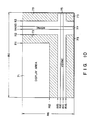
- Fig. 7 shows an example of display timing signal generating parameters for the CRT.
- the correspondence between parameters R0 via R16, shown in Fig. 7, and the display screen is shown in Fig. 10.
- reference numeral 71 denotes a display area; 73, border areas; and 77 and 75, horizontal and vertical sync periods, respectively.
- parameter R0 represents a total horizontal period of the display screen.
- Parameter R1 represents the end timing of a horizontal display period.
- Parameters R2 and R3 represent the start and end timings of a horizontal blank period, respectively.
- Parameters R2 and R3 constitute a boundary control parameter.
- Parameters R4 and R5 represent start and end timings of a horizontal sync signal, respectively.
- Parameter R6 represents a total vertical period of the display screen.
- Parameter R7 represents the overflowing portion of the parameter when the parameter is too lengthy to be stored in a single register.
- Parameters R10 and R11 represent the start and end timings of a vertical sync signal, respectively.
- Parameter R12 represents the end timing of a vertical display.
- parameters R15 and R16 represent the start and end timings of a vertical blank period, respectively.
- a horizontal total parameter is set to be "5B”; a horizontal display end parameter, "4F”; a horizontal blank start parameter, "53”; a horizontal blank end parameter, "17”; an H sync start parameter, "50”; an H sync end parameter, "BA”; a vertical total parameter, "6C”; an overflow parameter, "1F”; a V sync start parameter, "5E”; a V sync end parameter, "2B”; a vertical display end parameter, "5D”; a vertical blank start parameter, "5F”; and a vertical blank end parameter, "0A”.
- the panel resolution of the plasma display apparatus is selected to be 720 x 400 dots
- data non-display areas each consisting of the same number of dots, are formed on the left and right and/or the upper and lower portions of the physical screen, so that the display screen is located at the center of the physical screen.
- the parameter stored in ROM 5 is also used for generating a display timing signal for forming the non-display area.
- Pallet data is used for converting display data for CRT color display read out from V-RAM 9 into tone display data for the plasma display. In this embodiment, 16 colors are expressed by four tonal levels.
- tonal level "0" is a nondisplay level having no luminance; "1", a tone having a low luminance level; and "3", a tone having a high luminance level.
- pallet data A for displaying the data non-display area at tonal level "0” and pallet data B for displaying the non-display area at tonal level “1” are stored in ROM 5, and one of these pallet data is selected and set in pallet 11 (to be described later).
- CRT controller (CRTC) 13 is connected to CPU 1 through system bus 3.
- CRTC 13 has display timing register 14.
- CRTC 13 generates a display timing signal based on the received parameter, and outputs the signal to pallet 11.
- CRTC 13 fetches display data DD from V-RAM 9, and supplies this data to pallet 11.
- Pallet 11 receives either pallet data A or B stored in ROM 5 through system bus 3 and converts display data for CRT color display read out from V-RAM 9 into four tonal levels of display data, and supplies it to plasma display 7.
- BIOS 21 is connected to system bus 3, and stores a display area control program shown in Fig. 8 and a display mode set routine (not shown).
- Keyboard 23 for inputting various data including a BIOS command is connected to system bus 3.
- CPU 1 executes the display area control processing routine in BIOS 21.
- BIOS 21 When the power switch of the system is turned on, CPU 1 executes the display area control processing routine in BIOS 21.
- CPU 1 sets a default mode (having a display resolution of 640 x 400 dots shown in Fig. 2C) as a display mode for plasma display 7. More specifically, CPU 1 reads out the display timing signal generating parameters (PD) in the default display mode from ROM 5, and sets the readout parameters in display timing register 14 of CRTC 13 through system bus 3.
- PD display timing signal generating parameters
- CPU 1 reads out the currently set pallet data from ROM 5, and sets the readout data in pallet 11 through system bus 3.
- CPU 1 protects a display timing. More specifically, CPU 1 supplies control signal E/D of logic "0" to flip-flop 17 through system bus 3.
- CPU 1 supplies the I/O device address of CRTC 13 to decoder 19 through system bus 3.
- Decoder 19 decodes the input I/O device address, and supplies clock signal C to the clock input terminal of flip-flop 17.
- flip-flop 17 is reset, and outputs a signal of logic "0" from its Q output terminal to one input terminal of AND gate 15. Therefore, even if a new display timing set command is input from CPU 1 to the other input terminal of AND gate 15 through system bus 3, AND gate 15 blocks supply of command A to CRTC 13.
- step 35 an application program is executed.
- the flow then advances to step 37.
- CPU 1 supplies display mode set command A to one input terminal of AND gate 15 through system bus 3, and executes the display mode set routine in BIOS 21. If it is determined in step 41 that the display mode is not altered, the flow advances to step 55, and CPU 1 executes initialization including clearing of V-RAM 9.
- step 41 determines whether the display mode is altered. If it is determined in step 41 that the display mode is altered, the flow advances to step 43, and CPU 1 controls flip-flop 17 and decoder 19, so that new display timing parameters can be set in display timing register 14. More specifically, CPU 1 supplies control data E/D of logic "1" to flip-flop 17 through system bus 3, and sets the I/O device address of CRTC 13 in decoder 19. As a result, decoder 19 decodes the input I/O device address, and supplies high-level clock signal C to the clock input terminal of flip-flop 17. As a result, flip-flop 17 is set in synchronism with clock signal C. Therefore, a high-level Q output signal is supplied from flip-flop 17 to the other input terminal of AND gate 15.
- step 45 CPU 1 discriminates the display mode. If the display mode is the default mode, i.e., if the display resolution is 720 x 350 dots, the flow advances to step 47. In step 47, CPU 1 reads out display timing signal generating parameters PD for 720 x 350 dots from ROM 5, and sets them in display timing register 14 of CRTC 13 through system bus 3. If it Is determined in step 45 that the display mode corresponds to 640 x 400 dots, the flow advances to step 49.
- step 49 display timing signal generating parameters PD for 640 x 400 dots are read out from ROM 5, and are set in display timing register 14 through system bus 3. Similarly, when the display mode corresponds to 640 x 350 dots, display timing signal generating parameters PD for 640 x 350 dots are read out from ROM 5, and are set in display timing register 14 through system bus 3.
- step 53 The same processing as in step 33 is executed in step 53 to protect the display timing.
- step 55 initialization including clearing of V-RAM 9 is executed.
- the flow then returns to step 35, and CPU 1 executes the next application program. In this manner, in one application program, the display timing signal generating parameters can be altered only once, and thereafter, are inhibited from being altered until the application program ends.
- the display screen when data is displayed on a plasma display apparatus using an application program developed for a CRT display apparatus, if a display mode is altered, the display screen can be set at the center of the plasma display apparatus.
- Display timing signal generating parameters (PD) having display timings for forming upper and lower nondisplay areas of 25 dots, as shown in Fig.
- ROM 5 read out from ROM 5, and are set in display timing register 14 of CRTC 13 through system bus 3.
- CRTC 13 generates display timing signals based on input parameters PD, and supplies the signals to plasma display apparatus 7 through pallet 11.
- display timing signal generating parameters (PD) having display timings for forming upper and lower nondisplay areas consisting of 25 dots and right and left nondisplay areas consisting of 40 dots are read out from ROM 5, and are set in display timing register 14 of CRTC 13 through system bus 3.
- CRTC 13 generates display timing signals based on input parameters PD, and supplies them to plasma display apparatus 7 through pallet 11.
- a screen having an effective display screen indicated by a hatched portion and having the same upper and lower, and right and left data nondisplay areas is formed on plasma display apparatus 7.
- step 61 of Fig. 9 CPU 1 sets plasma display apparatus 7 in the default display mode.
- step 63 CPU 1 inhibits alteration of the display mode.
- the flow then advances to step 65, and CPU 1 executes an application program. It is checked in step 67 if a boundary display switching command (a command from keyboard 23 or a command on a program) is input during execution of the application program. If YES in step 67, CPU 1 rewrites pallet data set in pallet 11 in step 69.
- a boundary display switching command a command from keyboard 23 or a command on a program
- pallet data A for displaying the data nondisplay area at a nondisplay level having no luminance (tone level "0")
- pallet data B for displaying the data nondisplay area in tone of low luminance level (tone level "1").
- pallet data B is set, it is rewritten to be pallet data A.
Landscapes
- Engineering & Computer Science (AREA)
- Physics & Mathematics (AREA)
- Computer Hardware Design (AREA)
- General Physics & Mathematics (AREA)
- Theoretical Computer Science (AREA)
- Plasma & Fusion (AREA)
- Computer Graphics (AREA)
- Radar, Positioning & Navigation (AREA)
- Remote Sensing (AREA)
- Control Of Indicators Other Than Cathode Ray Tubes (AREA)
- Controls And Circuits For Display Device (AREA)
- Control Of Gas Discharge Display Tubes (AREA)
Applications Claiming Priority (6)
| Application Number | Priority Date | Filing Date | Title |
|---|---|---|---|
| JP152703/87 | 1987-06-19 | ||
| JP15270387 | 1987-06-19 | ||
| JP62276052A JP2635627B2 (ja) | 1987-06-19 | 1987-10-31 | 表示制御方式 |
| JP62276051A JPH01105296A (ja) | 1987-06-19 | 1987-10-31 | フラットディスプレイの表示エリア切換制御方式 |
| JP276051/87 | 1987-10-31 | ||
| JP276052/87 | 1987-10-31 |
Publications (3)
| Publication Number | Publication Date |
|---|---|
| EP0295690A2 true EP0295690A2 (de) | 1988-12-21 |
| EP0295690A3 EP0295690A3 (de) | 1991-03-27 |
| EP0295690B1 EP0295690B1 (de) | 1994-11-30 |
Family
ID=27320330
Family Applications (1)
| Application Number | Title | Priority Date | Filing Date |
|---|---|---|---|
| EP88109670A Expired - Lifetime EP0295690B1 (de) | 1987-06-19 | 1988-06-16 | System zum Steuern der Anzeigezone für ein Plasmaanzeigegerät |
Country Status (4)
| Country | Link |
|---|---|
| US (1) | US4990902A (de) |
| EP (1) | EP0295690B1 (de) |
| KR (1) | KR910005368B1 (de) |
| DE (1) | DE3852215T2 (de) |
Cited By (6)
| Publication number | Priority date | Publication date | Assignee | Title |
|---|---|---|---|---|
| EP0456165A3 (en) * | 1990-05-07 | 1992-04-01 | Kabushiki Kaisha Toshiba | Color lcd display control system |
| WO1995025299A1 (en) * | 1994-03-14 | 1995-09-21 | Apple Computer, Inc. | System for managing the display of information in a computer |
| EP0807919A1 (de) * | 1996-05-13 | 1997-11-19 | Hitachi, Ltd. | Anzeigevorrichtung und -verfahren |
| EP1617404A3 (de) * | 2004-07-13 | 2009-07-01 | Samsung Electronics Co., Ltd. | Vorrichtung zum Anpassen der Größe eines Displays und zugehöriges Verfahren |
| US8809613B2 (en) | 2009-07-24 | 2014-08-19 | Saudi Basic Industries Corporation | Method for preparing linear alpha-olefins |
| US9593055B2 (en) | 2008-01-30 | 2017-03-14 | Saudi Basic Industries Corporation | Method for preparing linear alpha-olefins |
Families Citing this family (42)
| Publication number | Priority date | Publication date | Assignee | Title |
|---|---|---|---|---|
| DE3852149T2 (de) * | 1987-06-19 | 1995-04-06 | Toshiba Kawasaki Kk | Kathodenstrahlröhre-/Plasmaanzeigesteuergerät. |
| US5592194A (en) * | 1988-04-27 | 1997-01-07 | Seiko Epson Corporation | Display controller |
| JP2634866B2 (ja) * | 1988-07-19 | 1997-07-30 | 株式会社日立製作所 | 液晶表示装置 |
| US5293485A (en) * | 1988-09-13 | 1994-03-08 | Kabushiki Kaisha Toshiba | Display control apparatus for converting color/monochromatic CRT gradation into flat panel display gradation |
| US5285192A (en) * | 1988-09-16 | 1994-02-08 | Chips And Technologies, Inc. | Compensation method and circuitry for flat panel display |
| JP3126360B2 (ja) * | 1989-09-01 | 2001-01-22 | キヤノン株式会社 | 表示システム及びその表示制御方法 |
| US6124842A (en) * | 1989-10-06 | 2000-09-26 | Canon Kabushiki Kaisha | Display apparatus |
| JPH03164791A (ja) * | 1989-11-24 | 1991-07-16 | Hitachi Ltd | 映像表示装置 |
| KR940004138B1 (en) * | 1990-04-06 | 1994-05-13 | Canon Kk | Display apparatus |
| JPH0455890A (ja) * | 1990-06-25 | 1992-02-24 | Canon Inc | 画像データ制御装置及び表示システム |
| DE69123407T2 (de) * | 1990-09-06 | 1997-04-30 | Canon Kk | Elektronisches Gerät |
| JPH07101917B2 (ja) * | 1991-05-14 | 1995-11-01 | 富士ゼロックス株式会社 | 領域制御装置 |
| JP3211969B2 (ja) * | 1991-06-27 | 2001-09-25 | ソニー株式会社 | 表示装置 |
| JPH06318060A (ja) * | 1991-07-31 | 1994-11-15 | Toshiba Corp | 表示制御装置 |
| US5285197A (en) * | 1991-08-28 | 1994-02-08 | Nec Technologies, Inc. | Method and apparatus for automatic selection of scan rates for enhanced VGA-compatible monitors |
| DE4129459A1 (de) * | 1991-09-05 | 1993-03-11 | Thomson Brandt Gmbh | Verfahren und vorrichtung zur ansteuerung von matrixdisplays |
| JPH05119734A (ja) * | 1991-10-28 | 1993-05-18 | Canon Inc | 表示制御装置 |
| JPH05127616A (ja) * | 1991-10-31 | 1993-05-25 | Canon Inc | 電気光学表示装置および電気光学素子駆動装置 |
| KR940004737B1 (ko) * | 1991-11-22 | 1994-05-28 | 삼성전관 주식회사 | 슈퍼 브이지에이 모니터 인터페이스 회로 |
| EP0554975B1 (de) * | 1992-02-03 | 1999-03-31 | Hewlett-Packard Company | Gerätunabhängige Schnittstelle für graphische Anzeigegeräte |
| JP2735451B2 (ja) * | 1993-01-05 | 1998-04-02 | 日本電気株式会社 | マルチスキャン型液晶ディスプレイ装置 |
| JP2531426B2 (ja) * | 1993-02-01 | 1996-09-04 | 日本電気株式会社 | マルチスキャン型液晶ディスプレイ装置 |
| US5954560A (en) * | 1993-06-02 | 1999-09-21 | Spectron Corporation Of America, L.L.C. | Method for making a gas discharge flat-panel display |
| US5469021A (en) * | 1993-06-02 | 1995-11-21 | Btl Fellows Company, Llc | Gas discharge flat-panel display and method for making the same |
| JP3363529B2 (ja) * | 1993-07-22 | 2003-01-08 | 富士通株式会社 | 動画表示装置 |
| EP0674207B1 (de) * | 1993-09-09 | 2001-11-28 | Kabushiki Kaisha Toshiba | Anzeigevorrichtung |
| US5739808A (en) * | 1994-10-28 | 1998-04-14 | Canon Kabushiki Kaisha | Display control method and apparatus |
| US5977933A (en) * | 1996-01-11 | 1999-11-02 | S3, Incorporated | Dual image computer display controller |
| US5801678A (en) * | 1996-04-26 | 1998-09-01 | Industrial Technology Research Institute | Fast bi-linear interpolation pipeline |
| KR100190841B1 (ko) * | 1996-07-08 | 1999-06-01 | 윤종용 | 화면정보전송기능을 갖는 모니터화면제어장치 및 그 제어방법 |
| JP3813689B2 (ja) * | 1996-07-11 | 2006-08-23 | 株式会社東芝 | 表示装置及びその駆動方法 |
| TW312764B (en) * | 1997-02-05 | 1997-08-11 | Acer Peripherals Inc | Method and device for calibrating monitor mode |
| US7554510B1 (en) * | 1998-03-02 | 2009-06-30 | Ati Technologies Ulc | Method and apparatus for configuring multiple displays associated with a computing system |
| US6295048B1 (en) * | 1998-09-18 | 2001-09-25 | Compaq Computer Corporation | Low bandwidth display mode centering for flat panel display controller |
| US7158094B2 (en) * | 1998-10-30 | 2007-01-02 | Ati International Srl | Method and apparatus for supporting multiple displays |
| US6823525B1 (en) * | 2000-01-21 | 2004-11-23 | Ati Technologies Inc. | Method for displaying single monitor applications on multiple monitors driven by a personal computer |
| US20020067337A1 (en) * | 2000-12-01 | 2002-06-06 | Klink Kristopher Allyn | Liquid crystal display imager and clock reduction method |
| JP2004205725A (ja) * | 2002-12-25 | 2004-07-22 | Semiconductor Energy Lab Co Ltd | 表示装置および電子機器 |
| US7180531B2 (en) * | 2004-02-27 | 2007-02-20 | Microsoft Corporation | Method and apparatus for enabling application program compatibility with display devices having improved pixel density |
| TWI236657B (en) * | 2004-09-01 | 2005-07-21 | Au Optronics Corp | Timing controller with external interface and apparatuses based thereon |
| US20100033509A1 (en) * | 2007-03-01 | 2010-02-11 | Panasonic Corporation | Image display device |
| US20110166968A1 (en) * | 2010-01-06 | 2011-07-07 | Richard Yin-Ching Houng | System and method for activating display device feature |
Family Cites Families (18)
| Publication number | Priority date | Publication date | Assignee | Title |
|---|---|---|---|---|
| US3928845A (en) * | 1974-12-11 | 1975-12-23 | Rca Corp | Character generator system selectively providing different dot-matrix size symbols |
| US4121283A (en) * | 1977-01-17 | 1978-10-17 | Cromemco Inc. | Interface device for encoding a digital image for a CRT display |
| JPS56122132U (de) * | 1980-02-18 | 1981-09-17 | ||
| US4454593A (en) * | 1981-05-19 | 1984-06-12 | Bell Telephone Laboratories, Incorporated | Pictorial information processing technique |
| US4422163A (en) * | 1981-09-03 | 1983-12-20 | Vend-A-Copy, Inc. | Power down circuit for data protection in a microprocessor-based system |
| DE3206451A1 (de) * | 1982-02-23 | 1983-09-08 | Siemens AG, 1000 Berlin und 8000 München | Verfahren zur reduzierung der untergrundhelligkeit im unteren bildbereich einer gasentladungsanzeigevorrichtung |
| US4536856A (en) * | 1982-06-07 | 1985-08-20 | Sord Computer Systems, Inc. | Method of and apparatus for controlling the display of video signal information |
| US4574279A (en) * | 1982-11-03 | 1986-03-04 | Compaq Computer Corporation | Video display system having multiple selectable screen formats |
| US4566005A (en) * | 1983-03-07 | 1986-01-21 | International Business Machines Corporation | Data management for plasma display |
| US4562450A (en) * | 1983-03-07 | 1985-12-31 | International Business Machines Corporation | Data management for plasma display |
| JPS6085678A (ja) * | 1983-10-17 | 1985-05-15 | Canon Inc | 画像表示装置 |
| US4611203A (en) * | 1984-03-19 | 1986-09-09 | International Business Machines Corporation | Video mode plasma display |
| KR930009159B1 (ko) * | 1984-04-20 | 1993-09-23 | 가부시기가이샤 히다찌세이사꾸쇼 | 입력일체화 평면 디스플레이시스템 |
| US4628534A (en) * | 1984-07-06 | 1986-12-09 | Honeywell Information Systems Inc. | Method for changing the resolution of compressed image data |
| US4764975A (en) * | 1984-12-06 | 1988-08-16 | Dainippon Screen Mfg. Co., Ltd. | Method of and apparatus for compressing image data |
| JPS61213896A (ja) * | 1985-03-19 | 1986-09-22 | 株式会社 アスキ− | デイスプレイコントロ−ラ |
| JPH0736104B2 (ja) * | 1985-03-27 | 1995-04-19 | 株式会社アスキ− | デイスプレイコントロ−ラ |
| US4763279A (en) * | 1985-12-26 | 1988-08-09 | International Business Machines Corporation | Method and apparatus for converting dot matrix display data of one resolution to a format for displaying on a display device having a different resolution |
-
1988
- 1988-06-16 DE DE3852215T patent/DE3852215T2/de not_active Expired - Lifetime
- 1988-06-16 EP EP88109670A patent/EP0295690B1/de not_active Expired - Lifetime
- 1988-06-17 US US07/207,790 patent/US4990902A/en not_active Expired - Lifetime
- 1988-06-18 KR KR1019880007433A patent/KR910005368B1/ko not_active Expired
Cited By (9)
| Publication number | Priority date | Publication date | Assignee | Title |
|---|---|---|---|---|
| EP0456165A3 (en) * | 1990-05-07 | 1992-04-01 | Kabushiki Kaisha Toshiba | Color lcd display control system |
| US5448260A (en) * | 1990-05-07 | 1995-09-05 | Kabushiki Kaisha Toshiba | Color LCD display control system |
| WO1995025299A1 (en) * | 1994-03-14 | 1995-09-21 | Apple Computer, Inc. | System for managing the display of information in a computer |
| US5682529A (en) * | 1994-03-14 | 1997-10-28 | Apple Computer, Inc. | System for dynamically accommodating changes in display configuration by notifying changes to currently running application programs to generate information by application programs to conform to changed configuration |
| EP0807919A1 (de) * | 1996-05-13 | 1997-11-19 | Hitachi, Ltd. | Anzeigevorrichtung und -verfahren |
| US6151000A (en) * | 1996-05-13 | 2000-11-21 | Hitachi, Ltd. | Display apparatus and display method thereof |
| EP1617404A3 (de) * | 2004-07-13 | 2009-07-01 | Samsung Electronics Co., Ltd. | Vorrichtung zum Anpassen der Größe eines Displays und zugehöriges Verfahren |
| US9593055B2 (en) | 2008-01-30 | 2017-03-14 | Saudi Basic Industries Corporation | Method for preparing linear alpha-olefins |
| US8809613B2 (en) | 2009-07-24 | 2014-08-19 | Saudi Basic Industries Corporation | Method for preparing linear alpha-olefins |
Also Published As
| Publication number | Publication date |
|---|---|
| US4990902A (en) | 1991-02-05 |
| KR890001013A (ko) | 1989-03-17 |
| KR910005368B1 (ko) | 1991-07-29 |
| EP0295690A3 (de) | 1991-03-27 |
| EP0295690B1 (de) | 1994-11-30 |
| DE3852215T2 (de) | 1995-04-06 |
| DE3852215D1 (de) | 1995-01-12 |
Similar Documents
| Publication | Publication Date | Title |
|---|---|---|
| EP0295690A2 (de) | System zum Steuern der Anzeigezone für ein Plasmaanzeigegerät | |
| EP0295691B1 (de) | Anzeigemodusumschaltsystem für ein Plasmaanzeigegerät | |
| EP0295689B1 (de) | Anzeigesteuergerät für eine Kathodenstrahlröhre-/Plasmaanzeigeeinheit | |
| US4574277A (en) | Selective page disable for a video display | |
| US5784037A (en) | Display system | |
| JPH0830948B2 (ja) | イメージ表示装置 | |
| US5467470A (en) | Computer able to determine whether or not a display is connected to it, in accordance with the status data stored in a register, and method of detecting whether or not a display is connected to a computer | |
| US7176874B2 (en) | Controller and control method for liquid-crystal display panel, and liquid-crystal display device | |
| JPS5960480A (ja) | デイスプレイ装置 | |
| US6140992A (en) | Display control system which prevents transmission of the horizontal synchronizing signal for a predetermined period when the display state has changed | |
| US6028587A (en) | Display device for controlling display gradation in display dots by writing image data in image memory | |
| JPS642955B2 (de) | ||
| CA1235534A (en) | Crt display control system | |
| KR970003090B1 (ko) | 표시 데이터 기입제어장치 | |
| JP2761335B2 (ja) | 画面表示装置 | |
| US6239775B1 (en) | Driving circuit of plasma display panel | |
| JPH10232645A (ja) | 映像表示装置 | |
| CN100357877C (zh) | 荧屏显示的控制方法 | |
| JP3461063B2 (ja) | 文字表示装置 | |
| JP2635627B2 (ja) | 表示制御方式 | |
| JP3789537B2 (ja) | キャラクタエリアアクセス制御回路 | |
| JP2674145B2 (ja) | 表示制御装置 | |
| JPH1185123A (ja) | カーソル表示制御回路 | |
| KR100214836B1 (ko) | Pdp-tv의 정지화상 표시장치. | |
| KR20000014526A (ko) | 저해상도 화상 데이터를 확대 표시하는 고해상도 액정 표시 장치 및 그 방법 |
Legal Events
| Date | Code | Title | Description |
|---|---|---|---|
| PUAI | Public reference made under article 153(3) epc to a published international application that has entered the european phase |
Free format text: ORIGINAL CODE: 0009012 |
|
| 17P | Request for examination filed |
Effective date: 19880713 |
|
| AK | Designated contracting states |
Kind code of ref document: A2 Designated state(s): DE FR GB |
|
| PUAL | Search report despatched |
Free format text: ORIGINAL CODE: 0009013 |
|
| AK | Designated contracting states |
Kind code of ref document: A3 Designated state(s): DE FR GB |
|
| 17Q | First examination report despatched |
Effective date: 19930315 |
|
| GRAA | (expected) grant |
Free format text: ORIGINAL CODE: 0009210 |
|
| AK | Designated contracting states |
Kind code of ref document: B1 Designated state(s): DE FR GB |
|
| REF | Corresponds to: |
Ref document number: 3852215 Country of ref document: DE Date of ref document: 19950112 |
|
| ET | Fr: translation filed | ||
| PLBE | No opposition filed within time limit |
Free format text: ORIGINAL CODE: 0009261 |
|
| STAA | Information on the status of an ep patent application or granted ep patent |
Free format text: STATUS: NO OPPOSITION FILED WITHIN TIME LIMIT |
|
| 26N | No opposition filed | ||
| REG | Reference to a national code |
Ref country code: GB Ref legal event code: IF02 |
|
| PGFP | Annual fee paid to national office [announced via postgrant information from national office to epo] |
Ref country code: DE Payment date: 20070614 Year of fee payment: 20 |
|
| PGFP | Annual fee paid to national office [announced via postgrant information from national office to epo] |
Ref country code: GB Payment date: 20070613 Year of fee payment: 20 |
|
| PGFP | Annual fee paid to national office [announced via postgrant information from national office to epo] |
Ref country code: FR Payment date: 20070608 Year of fee payment: 20 |
|
| REG | Reference to a national code |
Ref country code: GB Ref legal event code: PE20 Expiry date: 20080615 |
|
| PG25 | Lapsed in a contracting state [announced via postgrant information from national office to epo] |
Ref country code: GB Free format text: LAPSE BECAUSE OF EXPIRATION OF PROTECTION Effective date: 20080615 |