EP0300524A1 - Regelbares Dämpfungsglied zum Einfügen zwischen einem Emitterkreis und einem Belastungskreis - Google Patents
Regelbares Dämpfungsglied zum Einfügen zwischen einem Emitterkreis und einem Belastungskreis Download PDFInfo
- Publication number
- EP0300524A1 EP0300524A1 EP88201248A EP88201248A EP0300524A1 EP 0300524 A1 EP0300524 A1 EP 0300524A1 EP 88201248 A EP88201248 A EP 88201248A EP 88201248 A EP88201248 A EP 88201248A EP 0300524 A1 EP0300524 A1 EP 0300524A1
- Authority
- EP
- European Patent Office
- Prior art keywords
- circuit
- attenuation
- variable
- diodes
- parallel
- Prior art date
- Legal status (The legal status is an assumption and is not a legal conclusion. Google has not performed a legal analysis and makes no representation as to the accuracy of the status listed.)
- Granted
Links
- 230000037431 insertion Effects 0.000 title 1
- 238000003780 insertion Methods 0.000 title 1
- 230000006978 adaptation Effects 0.000 claims description 4
- 239000000969 carrier Substances 0.000 claims description 2
- 239000003990 capacitor Substances 0.000 description 7
- 238000010586 diagram Methods 0.000 description 2
- 238000002955 isolation Methods 0.000 description 2
- 230000000903 blocking effect Effects 0.000 description 1
- 238000012886 linear function Methods 0.000 description 1
Images
Classifications
-
- H—ELECTRICITY
- H03—ELECTRONIC CIRCUITRY
- H03H—IMPEDANCE NETWORKS, e.g. RESONANT CIRCUITS; RESONATORS
- H03H7/00—Multiple-port networks comprising only passive electrical elements as network components
- H03H7/24—Frequency- independent attenuators
- H03H7/25—Frequency- independent attenuators comprising an element controlled by an electric or magnetic variable
- H03H7/253—Frequency- independent attenuators comprising an element controlled by an electric or magnetic variable the element being a diode
- H03H7/255—Frequency- independent attenuators comprising an element controlled by an electric or magnetic variable the element being a diode the element being a PIN diode
Definitions
- the present invention relates to a variable attenuation device intended to be inserted between a transmitter circuit having a certain internal impedance and a load circuit, device formed by at least one parallel attenuation branch formed from a resistance element.
- variable PIN diode
- a bias circuit to vary the resistance of the element as a function of an attenuation control quantity.
- Such devices are well known and find important applications in particular as an amplitude modulator of a radio transmitter, the modulation acting as an attenuation control quantity. Efforts are made in this type of application, in order to obtain good modulation dynamics, to be able to withstand relatively high powers of the transmitter circuit.
- the object of the present invention is to provide an attenuation device capable of withstanding high power.
- the parallel attenuation branch comprises a dissipative element which is placed in series with the variable resistance element and whose value ensures the adaptation of the internal impedance of the transmitter circuit.
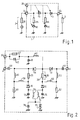
- Figure 1 shows the block diagram of the attenuation device according to the invention.
- FIG. 2 represents the diagram of the preferred embodiment of the attenuation device according to the invention.
- the reference 1 indicates the attenuation device to be inserted between an emitter circuit 2 which is connected between the input terminal 4 and the earth and a load circuit 5 which is connected between the output terminal 6 and the earth.
- the device is made up of P.I.N. 10, 11, 12 and 13 placed either in parallel (diodes 10 and 12), or in series (diodes 11 and 13).
- a bias circuit has been provided, shown simply in dotted lines in this FIG. 1, which allows the PIN diodes to be suitably biased from a control voltage applied to the control terminal. 20.
- resistive elements 25 and 26 have been arranged in series with the diodes 10 and 12 and the value of the resistance of these elements is such that it ensures both the adaptation of the internal resistance of the emitter circuit 2 , represented by the reference 30, than that of the charging circuit 5.
- FIG. 2 shows the embodiment of the device and details the diode bias circuit 10, 11, 12, 13 well.
- the references representing the elements already described in FIG. 1 remain unchanged.
- a first isolation capacitor 40 has been arranged between terminal 4 and the cathode of the diode 11 and a second isolation capacitor. 41 between terminal 6 and the cathode of diode 13.
- the anodes of diodes 11 and 13 are connected to terminal 20 by means of a blocking inductor 42 and an RC circuit formed by a resistor 43 and a capacitor 45 in parallel.
- a capacitor 48 connects the common point of the choke 42 and the RC circuit to ground.
- the anodes of diodes 11 and 13 are connected to ground for direct current via element 26, by a choke 50 and a resistor 52.
- the cathode of diode 13 is connected to ground via of a choke 55 and of the aforementioned resistor 52.
- the cathode of the diode 11 is connected to the earth always with regard to the direct current by means of a first circuit formed of the element 25, of a inductor 58 and a resistor 60 and a second circuit formed by an inductor 62 and the aforementioned resistor 60.
- the anodes of diodes 10 and 12 receive a DC voltage from a voltage generator 69 and via inductors 70 and 72 respectively.
- Capacitors 73 and 75 connected between the anodes of diodes 10 and 12 provide a path to earth for high frequency currents. It is also possible to provide for the connection of a capacitor 78 in parallel on the generator 69.
- the applicant has noticed that by connecting a capacitor 80 of relatively low capacity across the terminals of element 26, the adaptation of the device.
- the generator 69 supplies, in the absence of control voltage to terminal 20, a voltage such that the diodes 10 and 12 are in the on state and the diodes 11 and 13 in the state blocked; the attenuation is then maximum, the emitter circuit 2 is looped by the element 25 whose value corresponds to its internal resistance.
- the diodes 11 and 13 start to drive and the diodes 10 and 12 are less busy.
- the diodes 11 and 13 are completely on and the diodes 10 and 12 completely blocked, the attenuation is minimal.
- the R.O.S. (standing wave ratio) remains less than 1.6 for an attenuation varying from less than 2 dB to more than 50 dB - the power at the input being several watts - modulation frequencies ranging from 0 to 25 kHz with a voltage at terminal 20 ranging from 0 to 10 Volts.
- the attenuation is not a linear function of the voltage applied to the control terminal 20 and it is up to the user to provide, before terminal 20, any non-linear circuit which will give it the characteristic d desired attenuation.
Landscapes
- Attenuators (AREA)
- Transmitters (AREA)
Applications Claiming Priority (2)
| Application Number | Priority Date | Filing Date | Title |
|---|---|---|---|
| FR8709208A FR2617655B1 (fr) | 1987-06-30 | 1987-06-30 | Dispositif d'attenuation variable destine a etre insere entre un circuit emetteur et un circuit de charge |
| FR8709208 | 1987-06-30 |
Publications (2)
| Publication Number | Publication Date |
|---|---|
| EP0300524A1 true EP0300524A1 (de) | 1989-01-25 |
| EP0300524B1 EP0300524B1 (de) | 1993-09-08 |
Family
ID=9352676
Family Applications (1)
| Application Number | Title | Priority Date | Filing Date |
|---|---|---|---|
| EP88201248A Expired - Lifetime EP0300524B1 (de) | 1987-06-30 | 1988-06-17 | Regelbares Dämpfungsglied zum Einfügen zwischen einem Emitterkreis und einem Belastungskreis |
Country Status (5)
| Country | Link |
|---|---|
| US (1) | US4942375A (de) |
| EP (1) | EP0300524B1 (de) |
| JP (1) | JPS6432713A (de) |
| DE (1) | DE3883883T2 (de) |
| FR (1) | FR2617655B1 (de) |
Cited By (3)
| Publication number | Priority date | Publication date | Assignee | Title |
|---|---|---|---|---|
| FR2676150A1 (fr) * | 1991-05-03 | 1992-11-06 | Thomson Csf | Circuit attenuateur limiteur commandable a diode a zone intermediaire asga et utilisation d'un tel circuit. |
| US6362704B1 (en) | 1998-10-07 | 2002-03-26 | Nokia Corporation | Circuit arrangement improving the control characteristics of an attenuator |
| RU2354016C1 (ru) * | 2007-08-06 | 2009-04-27 | Открытое акционерное общество "ОКБ-Планета" | Ограничитель мощности свч |
Families Citing this family (14)
| Publication number | Priority date | Publication date | Assignee | Title |
|---|---|---|---|---|
| JPH0475423U (de) * | 1990-11-14 | 1992-07-01 | ||
| US5332981A (en) * | 1992-07-31 | 1994-07-26 | Emc Technology, Inc. | Temperature variable attenuator |
| US5345123A (en) * | 1993-07-07 | 1994-09-06 | Motorola, Inc. | Attenuator circuit operating with single point control |
| JP3063513B2 (ja) * | 1994-02-10 | 2000-07-12 | 松下電器産業株式会社 | マイクロ波検波給電回路 |
| SE508506C2 (sv) * | 1997-02-25 | 1998-10-12 | Ericsson Telefon Ab L M | Anordning och förfarande vid telekommunikation |
| US6144265A (en) * | 1997-11-26 | 2000-11-07 | Honeywell Inc. | Calibrated high power radio frequency step attenuator |
| US5969561A (en) * | 1998-03-05 | 1999-10-19 | Diablo Research Company, Llc | Integrated circuit having a variable RF resistor |
| KR20000045594A (ko) * | 1998-12-30 | 2000-07-25 | 김영환 | 초단파 및 극초단파 대역용 소형 가변 감쇠기 |
| US6919774B2 (en) * | 2001-10-03 | 2005-07-19 | Microtune (Texas), L.P. | Broadband PIN diode attenuator bias network |
| DE10234479A1 (de) * | 2002-07-29 | 2004-02-12 | Infineon Technologies Ag | Übertragungssystem |
| US8212648B2 (en) * | 2004-10-13 | 2012-07-03 | Yantel Corporation | Variable attenuator |
| WO2010095296A1 (ja) | 2009-02-20 | 2010-08-26 | 株式会社村田製作所 | 抵抗記憶素子およびその使用方法 |
| WO2010095295A1 (ja) | 2009-02-20 | 2010-08-26 | 株式会社村田製作所 | 抵抗記憶素子およびその使用方法 |
| US8903344B2 (en) * | 2010-11-30 | 2014-12-02 | Qualcomm Incorporated | Programmable attenuator |
Citations (3)
| Publication number | Priority date | Publication date | Assignee | Title |
|---|---|---|---|---|
| DE2912434A1 (de) * | 1979-03-29 | 1980-10-09 | Bosch Gmbh Robert | Vorrichtung zur amplitudenregelung hochfrequenter signale |
| US4378536A (en) * | 1981-06-09 | 1983-03-29 | Rca Corporation | High power, low frequency, electronically adjustable attenuator |
| US4621244A (en) * | 1984-05-17 | 1986-11-04 | At&T Bell Laboratories | Broadband variable attenuator using transmission lines series coupled by adjustable pin diodes |
Family Cites Families (16)
| Publication number | Priority date | Publication date | Assignee | Title |
|---|---|---|---|---|
| US3529266A (en) * | 1968-08-12 | 1970-09-15 | Us Army | Continuously and dynamically variable pin diode attenuator |
| US3846724A (en) * | 1973-07-25 | 1974-11-05 | Saba Gmbh | Adjustable attenuator with p-i-n diodes |
| NL7506265A (nl) * | 1975-05-28 | 1976-11-30 | Philips Nv | Regelbare hf-signaalverzwakker. |
| US4097827A (en) * | 1977-02-04 | 1978-06-27 | The United States Of America As Represented By The Secretary Of The Air Force | Constant impedance, constant phase pin diode with attenuator |
| US4216445A (en) * | 1978-12-22 | 1980-08-05 | The United States Of America As Represented By The Secretary Of The Army | Variable resistance attenuator |
| US4236126A (en) * | 1979-04-25 | 1980-11-25 | Cincinnati Electronics Corporation | Variable RF attenuator |
| SU866618A1 (ru) * | 1980-01-18 | 1981-09-23 | Предприятие П/Я В-2640 | Электрически управл емый аттенюатор |
| JPS5744314A (en) * | 1980-08-29 | 1982-03-12 | Nec Corp | Variable attenuator |
| JPS59216311A (ja) * | 1983-05-24 | 1984-12-06 | Matsushita Electric Ind Co Ltd | 可変抵抗減衰器 |
| JPS60160716A (ja) * | 1984-02-01 | 1985-08-22 | Nec Corp | 電圧制御減衰器 |
| JPS60260220A (ja) * | 1984-06-06 | 1985-12-23 | Sharp Corp | Rf可変減衰回路 |
| JPH0247127B2 (ja) * | 1984-06-13 | 1990-10-18 | Nippon Electric Co | Daioodogensuiki |
| JPS6173054A (ja) * | 1984-09-17 | 1986-04-15 | メデイカル テクノロジ− コ−ポレ−シヨン | 試料調整用小瓶 |
| SU1293773A1 (ru) * | 1985-04-01 | 1987-02-28 | Предприятие П/Я В-8150 | Электрически управл емый аттенюатор |
| JPH0672837B2 (ja) * | 1985-12-25 | 1994-09-14 | アンドレアス・スツアバドス | ペースト状試料物質用の検査容器 |
| JPS62200809A (ja) * | 1986-02-28 | 1987-09-04 | Fujitsu Ltd | 電圧制御形可変減衰器 |
-
1987
- 1987-06-30 FR FR8709208A patent/FR2617655B1/fr not_active Expired - Fee Related
-
1988
- 1988-06-17 EP EP88201248A patent/EP0300524B1/de not_active Expired - Lifetime
- 1988-06-17 DE DE88201248T patent/DE3883883T2/de not_active Expired - Fee Related
- 1988-06-28 JP JP63158210A patent/JPS6432713A/ja active Pending
-
1989
- 1989-09-15 US US07/408,455 patent/US4942375A/en not_active Expired - Fee Related
Patent Citations (3)
| Publication number | Priority date | Publication date | Assignee | Title |
|---|---|---|---|---|
| DE2912434A1 (de) * | 1979-03-29 | 1980-10-09 | Bosch Gmbh Robert | Vorrichtung zur amplitudenregelung hochfrequenter signale |
| US4378536A (en) * | 1981-06-09 | 1983-03-29 | Rca Corporation | High power, low frequency, electronically adjustable attenuator |
| US4621244A (en) * | 1984-05-17 | 1986-11-04 | At&T Bell Laboratories | Broadband variable attenuator using transmission lines series coupled by adjustable pin diodes |
Non-Patent Citations (1)
| Title |
|---|
| ELECTRONIC DESIGN, vol. 25, no. 7, 29 mars 1977, pages 100-102, Rochelle Park, US; R.S. VILES: "Need a PIN-diode attenuator" * |
Cited By (3)
| Publication number | Priority date | Publication date | Assignee | Title |
|---|---|---|---|---|
| FR2676150A1 (fr) * | 1991-05-03 | 1992-11-06 | Thomson Csf | Circuit attenuateur limiteur commandable a diode a zone intermediaire asga et utilisation d'un tel circuit. |
| US6362704B1 (en) | 1998-10-07 | 2002-03-26 | Nokia Corporation | Circuit arrangement improving the control characteristics of an attenuator |
| RU2354016C1 (ru) * | 2007-08-06 | 2009-04-27 | Открытое акционерное общество "ОКБ-Планета" | Ограничитель мощности свч |
Also Published As
| Publication number | Publication date |
|---|---|
| FR2617655B1 (fr) | 1994-05-20 |
| FR2617655A1 (fr) | 1989-01-06 |
| EP0300524B1 (de) | 1993-09-08 |
| DE3883883T2 (de) | 1994-04-14 |
| JPS6432713A (en) | 1989-02-02 |
| US4942375A (en) | 1990-07-17 |
| DE3883883D1 (de) | 1993-10-14 |
Similar Documents
| Publication | Publication Date | Title |
|---|---|---|
| EP0300524B1 (de) | Regelbares Dämpfungsglied zum Einfügen zwischen einem Emitterkreis und einem Belastungskreis | |
| EP0348283A1 (de) | Frequenzvervielfacher mit einem programmierbaren Koeffizienten | |
| EP0660512A1 (de) | Phasenschiebverstärker und seine Verwendung in einer Zusammenführungsschaltung | |
| EP0720292A1 (de) | Mobilfunkendgerät mit einem Schaltkreis | |
| FR3013537A1 (fr) | Commande de condensateur bst | |
| EP0612141B1 (de) | Leistungsregelungsverfahren und -vorrichtung für eine Schaltung mit einem Resonanzumrichter | |
| EP0377205B1 (de) | Strombegrenzer und seine Verwendung in einem optischen Empfänger | |
| FR2737065A1 (fr) | Dispositif semiconducteur incluant un amplificateur de puissance et appareil de telecommunication mobile incluant un tel dispositif semiconducteur | |
| FR2460576A1 (fr) | Circuit d'alimentation a trois bornes pour appareil telephonique | |
| EP0277855B1 (de) | Binärer-bipolarer Umsetzer | |
| EP0301635B1 (de) | Schaltvorrichtung für Hochfrequenzsignale | |
| EP0203663B1 (de) | Hyperfrequenzleistungsoszillator, der in einem grossen Frequenzgebiet linear moduliert ist | |
| EP0120756B1 (de) | Hochfrequenzbandpassverstärker mit einem eine anpassbare Impedanz enthaltenden Oszillator | |
| FR2581275A1 (fr) | Recepteur de signaux optiques a tres large bande. | |
| EP0046421B1 (de) | Empfänger für Signalübertragungssystem mittels elektromagnetischer, insbesondere infraroter Strahlung | |
| EP0103520B1 (de) | Eingangs- und Speisungsschaltung für einen Filter, insbesondere einen Filter für einen Rundsteuerungsempfänger | |
| EP0119927A1 (de) | Hochspannungsverstärker für kapazitive Last | |
| FR2532799A1 (fr) | Filtre passe-haut a condensateur commute | |
| EP0021909A1 (de) | Stabilisierter Hyperfrequenzoszillator mit Frequenzumsetzung und seine Festkörperausführung | |
| EP0165640A1 (de) | Vorrichtung zur galvanischen Isolierung zwischen einem Impulsgeber und einer Belastung | |
| FR2473230A1 (fr) | Generateur de signaux electriques a puissance elevee | |
| WO2023144200A1 (fr) | Amplificateur audio haute performance | |
| EP0166643A1 (de) | Taktstarkstromzuführung | |
| FR2605816A1 (fr) | Oscillateur hyperfrequence a transistor, accordable par tension et generateur hyperfrequence a large bande comportant de tels oscillateurs | |
| CH631034A5 (en) | Modulation circuit |
Legal Events
| Date | Code | Title | Description |
|---|---|---|---|
| PUAI | Public reference made under article 153(3) epc to a published international application that has entered the european phase |
Free format text: ORIGINAL CODE: 0009012 |
|
| AK | Designated contracting states |
Kind code of ref document: A1 Designated state(s): DE FR GB IT SE |
|
| 17P | Request for examination filed |
Effective date: 19890713 |
|
| 17Q | First examination report despatched |
Effective date: 19910812 |
|
| ITTA | It: last paid annual fee | ||
| GRAA | (expected) grant |
Free format text: ORIGINAL CODE: 0009210 |
|
| AK | Designated contracting states |
Kind code of ref document: B1 Designated state(s): DE FR GB IT SE |
|
| REF | Corresponds to: |
Ref document number: 3883883 Country of ref document: DE Date of ref document: 19931014 |
|
| ITF | It: translation for a ep patent filed | ||
| GBT | Gb: translation of ep patent filed (gb section 77(6)(a)/1977) |
Effective date: 19931207 |
|
| PLBE | No opposition filed within time limit |
Free format text: ORIGINAL CODE: 0009261 |
|
| STAA | Information on the status of an ep patent application or granted ep patent |
Free format text: STATUS: NO OPPOSITION FILED WITHIN TIME LIMIT |
|
| 26N | No opposition filed | ||
| EAL | Se: european patent in force in sweden |
Ref document number: 88201248.7 |
|
| ITPR | It: changes in ownership of a european patent |
Owner name: CAMBIO RAGIONE SOCIALE;PHILIPS ELECTRONICS N.V. |
|
| PGFP | Annual fee paid to national office [announced via postgrant information from national office to epo] |
Ref country code: FR Payment date: 19970620 Year of fee payment: 10 |
|
| PGFP | Annual fee paid to national office [announced via postgrant information from national office to epo] |
Ref country code: GB Payment date: 19980601 Year of fee payment: 11 |
|
| PGFP | Annual fee paid to national office [announced via postgrant information from national office to epo] |
Ref country code: SE Payment date: 19980625 Year of fee payment: 11 |
|
| PGFP | Annual fee paid to national office [announced via postgrant information from national office to epo] |
Ref country code: DE Payment date: 19980824 Year of fee payment: 11 |
|
| PG25 | Lapsed in a contracting state [announced via postgrant information from national office to epo] |
Ref country code: FR Free format text: LAPSE BECAUSE OF NON-PAYMENT OF DUE FEES Effective date: 19990226 |
|
| REG | Reference to a national code |
Ref country code: FR Ref legal event code: ST |
|
| PG25 | Lapsed in a contracting state [announced via postgrant information from national office to epo] |
Ref country code: GB Free format text: LAPSE BECAUSE OF NON-PAYMENT OF DUE FEES Effective date: 19990617 |
|
| PG25 | Lapsed in a contracting state [announced via postgrant information from national office to epo] |
Ref country code: SE Free format text: THE PATENT HAS BEEN ANNULLED BY A DECISION OF A NATIONAL AUTHORITY Effective date: 19990629 |
|
| GBPC | Gb: european patent ceased through non-payment of renewal fee |
Effective date: 19990617 |
|
| EUG | Se: european patent has lapsed |
Ref document number: 88201248.7 |
|
| PG25 | Lapsed in a contracting state [announced via postgrant information from national office to epo] |
Ref country code: DE Free format text: LAPSE BECAUSE OF NON-PAYMENT OF DUE FEES Effective date: 20000503 |
|
| PG25 | Lapsed in a contracting state [announced via postgrant information from national office to epo] |
Ref country code: IT Free format text: LAPSE BECAUSE OF NON-PAYMENT OF DUE FEES;WARNING: LAPSES OF ITALIAN PATENTS WITH EFFECTIVE DATE BEFORE 2007 MAY HAVE OCCURRED AT ANY TIME BEFORE 2007. THE CORRECT EFFECTIVE DATE MAY BE DIFFERENT FROM THE ONE RECORDED. Effective date: 20050617 |