EP0317124B1 - Silizium-auf-Isolator-Halbleiter-Komponenten, die dünne Schichten aus synthetischem Diamant enthalten - Google Patents
Silizium-auf-Isolator-Halbleiter-Komponenten, die dünne Schichten aus synthetischem Diamant enthalten Download PDFInfo
- Publication number
- EP0317124B1 EP0317124B1 EP88310313A EP88310313A EP0317124B1 EP 0317124 B1 EP0317124 B1 EP 0317124B1 EP 88310313 A EP88310313 A EP 88310313A EP 88310313 A EP88310313 A EP 88310313A EP 0317124 B1 EP0317124 B1 EP 0317124B1
- Authority
- EP
- European Patent Office
- Prior art keywords
- layer
- silicon
- diamond
- grooves
- semiconductor
- Prior art date
- Legal status (The legal status is an assumption and is not a legal conclusion. Google has not performed a legal analysis and makes no representation as to the accuracy of the status listed.)
- Expired - Lifetime
Links
Images


Classifications
-
- H—ELECTRICITY
- H10—SEMICONDUCTOR DEVICES; ELECTRIC SOLID-STATE DEVICES NOT OTHERWISE PROVIDED FOR
- H10P—GENERIC PROCESSES OR APPARATUS FOR THE MANUFACTURE OR TREATMENT OF DEVICES COVERED BY CLASS H10
- H10P14/00—Formation of materials, e.g. in the shape of layers or pillars
- H10P14/20—Formation of materials, e.g. in the shape of layers or pillars of semiconductor materials
- H10P14/29—Formation of materials, e.g. in the shape of layers or pillars of semiconductor materials characterised by the substrates
- H10P14/2901—Materials
- H10P14/2902—Materials being Group IVA materials
- H10P14/2903—Carbon, e.g. diamond-like carbon
-
- H—ELECTRICITY
- H10—SEMICONDUCTOR DEVICES; ELECTRIC SOLID-STATE DEVICES NOT OTHERWISE PROVIDED FOR
- H10P—GENERIC PROCESSES OR APPARATUS FOR THE MANUFACTURE OR TREATMENT OF DEVICES COVERED BY CLASS H10
- H10P14/00—Formation of materials, e.g. in the shape of layers or pillars
- H10P14/20—Formation of materials, e.g. in the shape of layers or pillars of semiconductor materials
- H10P14/29—Formation of materials, e.g. in the shape of layers or pillars of semiconductor materials characterised by the substrates
- H10P14/2901—Materials
- H10P14/2902—Materials being Group IVA materials
- H10P14/2905—Silicon, silicon germanium or germanium
-
- H—ELECTRICITY
- H10—SEMICONDUCTOR DEVICES; ELECTRIC SOLID-STATE DEVICES NOT OTHERWISE PROVIDED FOR
- H10P—GENERIC PROCESSES OR APPARATUS FOR THE MANUFACTURE OR TREATMENT OF DEVICES COVERED BY CLASS H10
- H10P14/00—Formation of materials, e.g. in the shape of layers or pillars
- H10P14/20—Formation of materials, e.g. in the shape of layers or pillars of semiconductor materials
- H10P14/32—Formation of materials, e.g. in the shape of layers or pillars of semiconductor materials characterised by intermediate layers between substrates and deposited layers
- H10P14/3202—Materials thereof
- H10P14/3204—Materials thereof being Group IVA semiconducting materials
- H10P14/3206—Carbon, e.g. diamond-like carbon
-
- H—ELECTRICITY
- H10—SEMICONDUCTOR DEVICES; ELECTRIC SOLID-STATE DEVICES NOT OTHERWISE PROVIDED FOR
- H10P—GENERIC PROCESSES OR APPARATUS FOR THE MANUFACTURE OR TREATMENT OF DEVICES COVERED BY CLASS H10
- H10P14/00—Formation of materials, e.g. in the shape of layers or pillars
- H10P14/20—Formation of materials, e.g. in the shape of layers or pillars of semiconductor materials
- H10P14/32—Formation of materials, e.g. in the shape of layers or pillars of semiconductor materials characterised by intermediate layers between substrates and deposited layers
- H10P14/3202—Materials thereof
- H10P14/3204—Materials thereof being Group IVA semiconducting materials
- H10P14/3211—Silicon, silicon germanium or germanium
-
- H—ELECTRICITY
- H10—SEMICONDUCTOR DEVICES; ELECTRIC SOLID-STATE DEVICES NOT OTHERWISE PROVIDED FOR
- H10P—GENERIC PROCESSES OR APPARATUS FOR THE MANUFACTURE OR TREATMENT OF DEVICES COVERED BY CLASS H10
- H10P14/00—Formation of materials, e.g. in the shape of layers or pillars
- H10P14/20—Formation of materials, e.g. in the shape of layers or pillars of semiconductor materials
- H10P14/32—Formation of materials, e.g. in the shape of layers or pillars of semiconductor materials characterised by intermediate layers between substrates and deposited layers
- H10P14/3242—Structure
- H10P14/3244—Layer structure
- H10P14/3251—Layer structure consisting of three or more layers
-
- H—ELECTRICITY
- H10—SEMICONDUCTOR DEVICES; ELECTRIC SOLID-STATE DEVICES NOT OTHERWISE PROVIDED FOR
- H10P—GENERIC PROCESSES OR APPARATUS FOR THE MANUFACTURE OR TREATMENT OF DEVICES COVERED BY CLASS H10
- H10P14/00—Formation of materials, e.g. in the shape of layers or pillars
- H10P14/20—Formation of materials, e.g. in the shape of layers or pillars of semiconductor materials
- H10P14/34—Deposited materials, e.g. layers
- H10P14/3402—Deposited materials, e.g. layers characterised by the chemical composition
- H10P14/3404—Deposited materials, e.g. layers characterised by the chemical composition being Group IVA materials
- H10P14/3411—Silicon, silicon germanium or germanium
-
- H—ELECTRICITY
- H10—SEMICONDUCTOR DEVICES; ELECTRIC SOLID-STATE DEVICES NOT OTHERWISE PROVIDED FOR
- H10P—GENERIC PROCESSES OR APPARATUS FOR THE MANUFACTURE OR TREATMENT OF DEVICES COVERED BY CLASS H10
- H10P14/00—Formation of materials, e.g. in the shape of layers or pillars
- H10P14/20—Formation of materials, e.g. in the shape of layers or pillars of semiconductor materials
- H10P14/34—Deposited materials, e.g. layers
- H10P14/3402—Deposited materials, e.g. layers characterised by the chemical composition
- H10P14/3414—Deposited materials, e.g. layers characterised by the chemical composition being group IIIA-VIA materials
- H10P14/3421—Arsenides
-
- H—ELECTRICITY
- H10—SEMICONDUCTOR DEVICES; ELECTRIC SOLID-STATE DEVICES NOT OTHERWISE PROVIDED FOR
- H10P—GENERIC PROCESSES OR APPARATUS FOR THE MANUFACTURE OR TREATMENT OF DEVICES COVERED BY CLASS H10
- H10P50/00—Etching of wafers, substrates or parts of devices
- H10P50/60—Wet etching
- H10P50/64—Wet etching of semiconductor materials
- H10P50/642—Chemical etching
-
- Y—GENERAL TAGGING OF NEW TECHNOLOGICAL DEVELOPMENTS; GENERAL TAGGING OF CROSS-SECTIONAL TECHNOLOGIES SPANNING OVER SEVERAL SECTIONS OF THE IPC; TECHNICAL SUBJECTS COVERED BY FORMER USPC CROSS-REFERENCE ART COLLECTIONS [XRACs] AND DIGESTS
- Y10—TECHNICAL SUBJECTS COVERED BY FORMER USPC
- Y10S—TECHNICAL SUBJECTS COVERED BY FORMER USPC CROSS-REFERENCE ART COLLECTIONS [XRACs] AND DIGESTS
- Y10S148/00—Metal treatment
- Y10S148/135—Removal of substrate
Definitions
- the present invention is directed to a method for making semiconductor elements comprising a single crystal layer of silicon on a diamond insulator.
- the present invention is further directed to novel semiconductor elements made according to that process.
- a component useful for integrated circuits is an active semiconductor film on an insulating substrate, since it has superior operational characteristics compared to a noninsulated active semiconductor film.
- a conventional noninsulated active semiconductor film made of silicon which itself is not an insulator, suffers from the problem of cross-talk, which is the transportation of charge carriers along the silicon substrate between adjacent transistors in an integrated circuit.
- silicon semiconductor films on insulators have been developed, which include the formation of single-crystal silicon films on insulating substrates such as sapphire, spinale and on amorphous silicon dioxide, followed by recrystallization of the polysilicon films.
- SOI silicon on insulator
- CMOS complementary metallic oxide semiconductor
- the problems with current SOI technology include the following.
- sapphire is used as the insulator
- the quality of epitaxial silicon films deposited on sapphire are inferior to conventional Czochralski crystals, or expitaxial films deposited on single-crystal silicon.
- Very thin (on the order of 1-2 micrometers) silicon epitaxial films are typically poor in quality with a large density of defects which severely limit the capabilities of circuits built with them.
- the achievement of high-quality thin epitaxial silicon films is required to maximize the advantage of SOI technology, but such thin films have heretofore not been achievable with acceptable performance.
- Silicon on sapphire technology is also extremely expensive since it requires the growth of a single sapphire crystal, slicing of the single crystals into wafers, polishing the wafers, and depositing the silicon on the wafers by CVD (chemical vapor deposition) techniques.
- CVD chemical vapor deposition
- the present invention provides semiconductor elements comprising a single crystal layer of silicon on a diamond insulator.
- a basic element is formed by the steps of diffusing into one surface of a substrate an etch-stop material which is not etchable by at least one etching process which etches the substrate, to form a diffusion-prepared layer; epitaxially depositing a silicon layer onto the diffusion prepared layer of the substrate; depositing a diamond layer onto the epitaxial silicon layer; removing the substrate by an etching process which does not etch the etch-stop material whereby the etching ceases at the diffusion-prepared layer; and selectively removing the diffusion-prepared layer to form the semiconductor element.
- a support layer may also be deposited upon the surface of the diamond insulator which is not in contact with the silicon layer. This basic element is further processed to provide novel semiconductor elements comprising single layers of silicon on diamond for various applications.
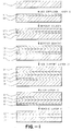
- FIG. 1 schematically shows the steps in a preferred embodiment according to the process of the present invention for making a semiconductor element comprising a single layer of silicon on a diamond film.
- FIG. 2 schematically shows the steps in a preferred embodiment for making a semiconductor element comprising silicon wafers separated by diamond insulator.
- FIG. 3 illustrates an embodiment of a semiconductor device embodying the silicon wafers shown in FIG. 2.
- FIG. 4 schematically shows the steps of the preferred embodiment for making gallium-arsenide wafers separated by silicon diamond insulators.
- FIG. 5 schematically shows the steps of a preferred embodiment for making stacked silicon semiconductors applicable for three-dimensional integrated circuits.
- the use of a silicon on a sapphire insulator as a semiconductor element is feasible because it is possible to grow a single-crystal sapphire which can be sliced into wafers and polished to provide an essentially smooth surface on which to grow a single crystal silicon layer.
- single-crystal diamonds made by synthetic routes are not feasible, and even if it would be possible to make a synthetic single-crystal diamond, there is a likelihood that the lattice mismatch between diamond and silicon would preclude the growth of a high-quality single-layer silicon on such a diamond surface. Therefore, the present invention provides a novel method for providing a single-crystal silicon layer on a synthetic diamond insulator where the single-crystal silicon is of suitable quality to serve as a semiconductor surface for integrated circuits.
- the first step is to apply etch-stop layer 11 to one surface of a substrate 10.
- etch-stop layer 11 will enable one at a later stage as described hereinbelow to etch away the substrate by an etching process which stops at the etch-stop layer.
- the substrate 10 will be a silicon wafer and one surface of it will be diffusion-prepared by diffusing a high concentration of boron into the surface to form etch-stop layer 11. Processes for diffusing boron into a silicon surface are known as, for example, B2H6 phase diffusion or ion implantation followed by annealing.
- silicon 12 is epitaxially deposited upon the diffusion-prepared layer by conventional methods.
- the processes for epitaxial deposition of silicon are well known.
- the thickness of the epitaxial silicon layer 12 will preferably be within the range of about 1-2 micrometers, which is a thickness useful for semiconductor applications.
- a layer of diamond 13 is deposited upon the epitaxial silicon film 12.
- the thickness of the diamond depends on whether the final structure is to be self-supporting, in which case the diamond layer should be deposited to the thickness of about 0.38 to 0.51 mm (15 to 20 mils), or if the final structure is to be supported by a substrate to be subsequently deposited upon the diamond layer as shown in FIG. 1. If a substrate is to ultimately support the structure, the diamond layer may be deposited in somewhat thinner thicknesses, such as in the range of 1 to 2 micrometers . Then a thicker polysilicon layer 14 may be deposited upon a diamond layer which will confer rigidity to the structure.
- etching process is utilized to etch away the substrate 10 (which is preferably silicon).
- the etching process is chosen such that the boron-diffused layer 11 will function as an etch-stop.
- Conventional etching reagents used for etching silicon include potassium hydroxide, mixtures of hydrofluoric acid and nitric acid, and a mixture of ethylenediamine-pyrocatechol-water.
- the epitaxial silicon film 12 is exposed by removing the etch-stop layer 11 which is preferably a diffused boron-silicon layer.
- the diffused boron-silicon layer 11 may be removed, for example, by ion etching or by selective oxidation with subsequent removal of the oxide, by known techniques.
- the resulting structure is a thin, high-quality single-crystal layer silicon (12) on insulating diamond (13).
- the bottom layer of the diamond may be supported by a supporting structure (14) such as polysilicon.
- this multilayer structure is utilized for application in the technology of radiation-hardened integrated circuits where there is the requirement for multiple single-crystal silicon elements electrically isolated from each other, typically provided by providing back-to-back diodes around regions of silicon wafers, forming individual silicon islands surrounded by moats.
- the air in the moats functions as a dielectric; or dielectric isolation is attained when each silicon wafer is fabricated in a manner such as to provide individual islands of silicon surrounded by a dielectric such as polysilicon.
- dielectric isolation is preferable because of the superior dielectric strength of polysilicon as compared to back-to-back diodes or air.
- a problem in the prior art is that the creation of dielectrically isolated wafers is complex and therefore it has heretofore been utilized mainly in only specialized applications.
- the present invention provides another embodiment of making silicon wafers isolated from each other by synthetic diamond.
- An advantage of the structure is the superior electrical resistivity and thermal conductivity of diamond.
- the preferred process for making such a device is shown in FIG. 2.
- a multilayer silicon on diamond component as fabricated, for example, as shown in connection with FIG. 1, is provided comprising the silicon layer 22 on the thin synthetic diamond film 23 supported on a support such as polysilicon 24.
- a predetermined pattern is etched into the silicon layer 22 forming grooves 25A, 25B, etc., of which the bottom surfaces 26A, 26B, etc. consist of unexposed area of the underlying synthetic diamond film 23.
- individual epitaxial silicon wafers 22A, 22B, 22C, etc. are formed.
- Synthetic diamond is then deposited around and over the epitaxial silicon islands 22A, 22B and 22C whereby the grooves 25A, 25B, etc. become solid diamond channels 27A, 27B, etc. and the silicon wafers 22A, 22B, 22C, etc. are covered with a thin diamond layer 27.
- a conventional photoresist 28 is then applied over the layer 27, then the photoresist is partially removed by utilizing the negative of the pattern used to form grooves 25A, 25B, etc. By removing the photoresist in this manner, photoresist islands 28A and 28B, etc. remain over the diamond channels 27A, 27B, etc., while the remainder of layer 27 becomes exposed.
- the exposed areas of layer 27 are then plasma etched to reveal the upper surfaces of the silicon wafers 22A, 22B, 22C, etc. Finally, the remaining photoresist islands 28A, 28B are removed to complete the fabrication of the dielectrically isolated silicon wafers, 22A, 22B, 22C separated by diamond channels 27A, 27B, etc., all of which overlay a synthetic diamond film 23 which in turn is supported by a substrate such as polysilicon 24.
- FIG. 3 One of the applications of a structure produced in accordance with the method described in connection with FIG. 2 is to form BIMOS circuits where bipolar power transistors are built adjacent to MOS devices.
- a device is shown in FIG. 3 where one of the silicon wafers 30 is shown as accommodating an MOS transistor 34 and the other silicon wafer 31 is shown as accommodating a bipolar power transistor 35. Wafers 30 and 31 and insulated from each other and from the support 33 by synthetic diamond layer 32.
- the silicon on diamond layers may be utilized to form components containing gallium-arsenide semiconductors.
- a particular problem with gallium-arsenide components is dealing with the dissipation of heat generated from the device.
- the present invention provides an advantage in that synthetic diamond may be utilized as a heat sink and in accordance with this aspect of the present invention a monolithic structure may be created in which the diamond forms an integral part of the gallium arsenide wafer.
- a thin silicon layer 42 on a synthetic diamond layer 43, which is in turn supported by support 44 is provided as, for example, in accordance with FIG. 1.
- a second diamond layer 45 is deposited upon the silicon layer 42. Then the diamond layer 45 is exposed to a predetermined pattern and etched, by processes described above, to provide islands of synthetic diamond 45A, 45B, 45C, 45D, etc. surrounded by exposed surfaces 42A, 42B, 42C, 42D, etc. of the silicon layer 42.
- the grooves between the diamond are then filled with gallium-arsenide by one of the conventional techniques for growing gallium-arsenide, such as liquid face epitaxy methods, chemical vapor deposition, and the like.
- the completed structure comprises on its upper surface, wafers of gallium-arsenide 46A, 46B, 46C, 46D, etc., separated by areas of diamond insulation, 45A, 45B, 45C, 45D, etc. all of which are in contact with a lower silicon layer 42.
- a silicon layer 42 is insulated from the support 44 by a diamond insulating layer 43.
- the diamond, 45A, 45B, etc., surrounding the gallium-arsenide and the diamond layer 43 beneath the silicon layer 42 function as heat sinks and dielectrics.
- the silicon layer 42 should be as thin as possible (on the order of less than 1 micrometer) to minimize the barrier effect to heat transfer between the gallium-arsenide wafers 46A, 46B, etc. and the diamond layer 43.
- the silicon on diamond components may be utilized to fabricate three-dimensional integrated circuits wherein active elements of the circuits are built on top of each other.
- One of the advantages of the present invention is that in building smaller circuits, the smaller device geometries call for thinner dielectrics, higher doping densities, shallower junctions and higher conductivities. These requirements become increasingly difficult to achieve because of material and device limitations.
- One of the advantages features in the present invention is that many of these inherent problems from scaling down conventional structures into three-dimensional integration become readily adaptable and practical utilizing diamond insulators in accordance with the present invention.
- FIG. 5 there is shown a silicon layer 52 on diamond insulating layer 53 on a support 54, as produced, for example, as shown in accordance with FIG. 1 above.
- a second layer of diamond 55 is deposited upon silicon layer 52.
- a pattern is etched into layer 55 (not shown) to form a series of diamond island 55A, 55B, 55C, etc. upon the silicon layer 52. Areas between the islands 55A, etc. are filled and the islands are covered simultaneously by depositing polysilicon 56 over the wafers 55A, etc.
- the polysilicon in then converted to a single crystal by seeded, lateral liquid phase epitaxial growth by, for example, laterally moving a strip heater 60 near the surface of the polysilicon 56.
- the same pattern utilized to form the islands 55A, 55B, 55C is utilized to etch through the single crystal layer 57 and the silicon layer 52 to form isolated stacks comprising single-crystal silicon 57A on diamond insulator 55A and second silicon layer 52A.
- the stacks are all in contact with a common diamond layer 53.
- the ultimate device comprises multiple layers of single-crystal interleaved with diamond for use in three-dimensional integrated circuits.
- the semiconductor elements according to the present invention may be used as semiconductor elements in integrated circuits with the problems of cross-talk and latch-up being essentially eliminated due to the presence of the insulating diamond layer. Moreover, the insulating diamond layer is obtained without the necessity of forming a single-crystal diamond by synthetic methods, which in any case would be technologically inachievable given the present state-of-the-art of diamond synthesis.
Landscapes
- Crystals, And After-Treatments Of Crystals (AREA)
- Element Separation (AREA)
- Recrystallisation Techniques (AREA)
- Formation Of Insulating Films (AREA)
- Thin Film Transistor (AREA)
- Carbon And Carbon Compounds (AREA)
- Laminated Bodies (AREA)
- Drying Of Semiconductors (AREA)
Claims (13)
- Verfahren zum Herstellen eines Halbleiterelements mit einer Einkristallschicht aus Silicium auf einem Isolator, welches die folgenden Schritte umfaßt:Hineindiffundieren eines Ätzschutzmaterials in eine Oberfläche eines Substrats (10), welches von mindestens einem Ätzvorgang nicht weggeätzt werden kann, bei dem das Substrat geätzt wird, wodurch eine durch Diffusion hergestellte Schicht (11) gebildet wird,epitaxisches Ablagern einer Siliciumschicht (12) auf der durch Diffusion hergestellten Schicht des Substrats,Vorsehen eines Isolators (13) auf der Siliciumschicht, Ablagern mindestens einer Stützschicht (14) auf dem Isolator,Entfernen des Substrats (10) durch einen Ätzvorgang, durch den das Ätzschutzmittel nicht weggeätzt wird, so daß das Ätzen an der durch Diffusion hergestellten Schicht aufhört, undwahlweise das Entfernen der durch Diffusion hergestellten Schicht (11), um das Halbleiterelement zu bilden, dadurch gekennzeichnet, daß der Isolator dadurch vorgesehen wird, daß eine Diamantschicht auf der Siliciumschicht abgelagert wird.
- Verfahren nach Anspruch 1, bei dem die Siliciumschicht (12) eine einheitliche Dicke aufweist, die in dem Bereich von 1 bis 2 Mikrometer liegt.
- Verfahren nach Anspruch 1 oder 2, bei dem das Substrat (10) Silicium umfaßt, und bei dem das Ätzschutzmaterial eine mit Bor diffundierte Schicht auf dem Siliciumsubstrat aufweist.
- Verfahren nach Anspruch 1, 2 oder 3, bei dem die Stützschicht (14) Polysilicium umfaßt.
- Verfahren zum Herstellen eines Halbleiterelements, welches eine Vielzahl von Siliciumscheiben umfaßt, die durch isolierende Diamantkanäle voneinander getrennt sind, wobei das Verfahren folgendes umfaßt:Herstellen eines mehrschichtigen Bauteils, das der Reihe nach eine Siliciumschicht (22), eine synthetische Diamantschicht (23) und eine Stützschicht (24) nach dem Verfahren eines der Ansprüche 1-4 umfaßt, wobei das Verfahren die folgenden weiteren Schritte umfaßt:Einätzen eines vorbestimmten Musters von Rillen (25a, 25b) in die Siliciumschicht, um ein entsprechendes belichtetes Muster auf einer Oberfläche der Diamantschichtablagerung zu bilden, wobei sich eine synthetische Diamantschicht auf der sich ergebenden Rillensiliciumfläche befindet, wobei die Rillen und die Siliciumfläche mit Diamant (27, 27a, 27b) gefüllt und abgedeckt werden, um verdeckte Inseln aus Silicium (22a, 22b, 22c) zu bilden,Auftragen eines Photoresistlacks (28) auf der sich ergebenden Diamantfläche und Belichten und Entwickeln des Photoresistlacks, wodurch der Photoresistlack (28b) nur auf den mit Diamant gefüllten Rillen verbleibt,Wegätzen des belichteten Diamantfilms, und Entfernen des verbleibenden Photoresistlacks.
- Verfahren zum Herstellen eines Halbleiterelements, das eine Vielzahl von Galliumarsenid-Scheiben auf einer gemeinsamen Siliciumschicht umfaßt, wobei jede Scheibe seitlich von angrenzenden Scheiben durch einen isolierenden synthetischen Diamantfilm getrennt ist, wobei das Verfahren die folgenden Schritte umfaßt:Herstellen eines mehrschichtigen Bauteils, das der Reihe nach eine erste synthetische Diamantschicht (45), eine Siliciumschicht (42), eine zweite synthetische Diamantschicht (43) und eine Stützschicht (44) gemäß einem Verfahren umfaßt, das die Schritte von jedem der Ansprüche 1-4 umfaßt, wobei dieses Verfahren die weiteren Schritte des Einätzens eines vorbestimmten Rillenmusters in die erste Diamantschicht, so daß die Oberfläche des Bodens der Rillen die Siliciumschicht umfaßt, und das Füllen der Rillen mit Galliumarsenid (46a, 46b, etc.) umfaßt.
- Verfahren zum Herstellen eines Halbleiterelements mit einer Vielzahl von gestapelten Halbleitern, wobei jeder dieser Stapel von dem anderen durch einen synthetischen Diamantfilm getrennt ist, und wobei benachbarte Stapel durch Luft oder durch ein geeignetes nichtleitendes Material getrennt sind, wobei das Verfahren die folgenden Schritte umfaßt: Herstellen eines mehrschichtigen Bauteils, das der Reihe nach eine erste synthetische Diamantschicht (53), eine Siliciumschicht (52) und eine zweite synthetische Diamantschicht (55) gemäß einem Verfahren umfaßt, das die Schritte eines der Ansprüche 1-4 beinhaltet, wobei das Verfahren die folgenden weiteren Schritte umfaßt: Einätzen eines vorbestimmten Musters von Rillen durch die zweite Diamantschicht zur Bildung von Rillen, wodurch die Oberfläche und der Boden der Rillen Silicium umfassen, Ablagern von Polysilicium (56), so daß die Rillen gefüllt werden und die zweite Diamantschicht von der Polysiliciumschicht überlagert wird, Aushärten des Polysiliciums mit Hitze, um einen einkristallinen Monolithen (57) zu bilden, Einätzen eines vorbestimmten Musters durch den Einkristall-Siliciummonolithen und die Siliciumschicht, um Mulden zu bilden, so daß die Oberflächen an dem Boden der Mulden die erste Diamantschicht umfassen.
- Halbleiterlement mit einem Halbleitermaterial (12), das von einem Substrat (14) getragen wird, dadurch gekennzeichnet, daß eine Diamantschicht (13) zwischen dem Halbleitermaterial und dem Substrat und im direkten Kontakt mit dem Halbleitermaterial angeordnet ist.
- Mehrschichtiges Halbleiterbauteil mit einer Vielzahl von Halbleiterelementen nach Anspruch 8, wobei das Halbleitermaterial in getrennten Abschnitten (22a, 22b, 22c) auf und in Kontakt mit der Diamantschicht (23) aufgebracht ist, die nebeneinanderliegend voneinander durch einen synthetischen Diamantfilm (27a, 27b) isoliert sind, um die Mehrzahl von Halbleiterelementen vorzusehen.
- Mehrschichtiges Halbleiterelektronikbauteil, das ein Halbleiterelement nach Anspruch 8 umfaßt, wobei das Halbleitermaterial Silicium ist und wobei eine mehrlagige Schicht auf der Siliciumschicht vorgesehen ist, wobei diese mehrlagige Schicht eine Scheibe aus Halbleitermaterial umfaßt, die durch eine Diamantisolierung (55) abgetrennt ist.
- Mehrschichtiges Halbleiterelektronikbauteil nach Anspruch 10, bei dem jede Scheibe der Reihe nach eine erste Siliciumscheibe in Kontakt mit der Diamantschicht, eine Diamantscheibe und eine zweite Siliciumscheibe umfaßt.
- Halbleiterkomponente nach einem der Ansprüche 8 bis 10, wobei das Substrat (14; 24) Polysilicium umfaßt.
- Komponente nach Anspruch 10, wobei das Halbleitermaterial, das durch eine Diamantisolierung abgetrennt ist, Galliumarsenid (46) umfaßt.
Applications Claiming Priority (2)
| Application Number | Priority Date | Filing Date | Title |
|---|---|---|---|
| US12130887A | 1987-11-16 | 1987-11-16 | |
| US121308 | 1987-11-16 |
Publications (3)
| Publication Number | Publication Date |
|---|---|
| EP0317124A2 EP0317124A2 (de) | 1989-05-24 |
| EP0317124A3 EP0317124A3 (en) | 1990-02-14 |
| EP0317124B1 true EP0317124B1 (de) | 1996-03-27 |
Family
ID=22395836
Family Applications (1)
| Application Number | Title | Priority Date | Filing Date |
|---|---|---|---|
| EP88310313A Expired - Lifetime EP0317124B1 (de) | 1987-11-16 | 1988-11-02 | Silizium-auf-Isolator-Halbleiter-Komponenten, die dünne Schichten aus synthetischem Diamant enthalten |
Country Status (5)
| Country | Link |
|---|---|
| US (1) | US5131963A (de) |
| EP (1) | EP0317124B1 (de) |
| JP (1) | JPH02110968A (de) |
| AT (1) | ATE136158T1 (de) |
| DE (1) | DE3855154D1 (de) |
Families Citing this family (61)
| Publication number | Priority date | Publication date | Assignee | Title |
|---|---|---|---|---|
| US4981818A (en) * | 1990-02-13 | 1991-01-01 | General Electric Company | Polycrystalline CVD diamond substrate for single crystal epitaxial growth of semiconductors |
| JP2542447B2 (ja) * | 1990-04-13 | 1996-10-09 | 三菱電機株式会社 | 太陽電池およびその製造方法 |
| WO1993001617A1 (en) * | 1991-07-08 | 1993-01-21 | Asea Brown Boveri Ab | Method for the manufacture of a semiconductor component |
| US5256581A (en) * | 1991-08-28 | 1993-10-26 | Motorola, Inc. | Silicon film with improved thickness control |
| JP3255960B2 (ja) * | 1991-09-30 | 2002-02-12 | 株式会社神戸製鋼所 | 冷陰極エミッタ素子 |
| US5561303A (en) * | 1991-11-07 | 1996-10-01 | Harris Corporation | Silicon on diamond circuit structure |
| US5276338A (en) * | 1992-05-15 | 1994-01-04 | International Business Machines Corporation | Bonded wafer structure having a buried insulation layer |
| US5300188A (en) * | 1992-11-13 | 1994-04-05 | Kobe Development Corp. | Process for making substantially smooth diamond |
| DE69225911T2 (de) * | 1992-12-18 | 1999-02-11 | Harris Corp., Melbourne, Fla. | Silizium-auf-diamant-schaltungsstruktur und herstellungsverfahren dafür |
| CA2113336C (en) * | 1993-01-25 | 2001-10-23 | David J. Larkin | Compound semi-conductors and controlled doping thereof |
| US5709745A (en) * | 1993-01-25 | 1998-01-20 | Ohio Aerospace Institute | Compound semi-conductors and controlled doping thereof |
| EP0616047B1 (de) * | 1993-02-16 | 1997-07-23 | Sumitomo Electric Industries, Limited | Polykristallines Substrat aus Diamant sowie Verfahren zur dessen Herstellung |
| US5272104A (en) * | 1993-03-11 | 1993-12-21 | Harris Corporation | Bonded wafer process incorporating diamond insulator |
| US5376579A (en) * | 1993-07-02 | 1994-12-27 | The United States Of America As Represented By The Secretary Of The Air Force | Schemes to form silicon-on-diamond structure |
| US5354717A (en) * | 1993-07-29 | 1994-10-11 | Motorola, Inc. | Method for making a substrate structure with improved heat dissipation |
| FR2708794B1 (fr) * | 1993-08-04 | 1995-09-15 | Pouyet Int | Module d'interconnexion rapide de deux lignes téléphoniques monopaires. |
| US5422901A (en) * | 1993-11-15 | 1995-06-06 | Motorola, Inc. | Semiconductor device with high heat conductivity |
| US5514242A (en) * | 1993-12-30 | 1996-05-07 | Saint Gobain/Norton Industrial Ceramics Corporation | Method of forming a heat-sinked electronic component |
| US5488350A (en) * | 1994-01-07 | 1996-01-30 | Michigan State University | Diamond film structures and methods related to same |
| US5474808A (en) * | 1994-01-07 | 1995-12-12 | Michigan State University | Method of seeding diamond |
| JP3353987B2 (ja) * | 1994-01-10 | 2002-12-09 | 株式会社半導体エネルギー研究所 | 素子作製方法 |
| US5554415A (en) * | 1994-01-18 | 1996-09-10 | Qqc, Inc. | Substrate coating techniques, including fabricating materials on a surface of a substrate |
| US5620754A (en) * | 1994-01-21 | 1997-04-15 | Qqc, Inc. | Method of treating and coating substrates |
| US5731046A (en) * | 1994-01-18 | 1998-03-24 | Qqc, Inc. | Fabrication of diamond and diamond-like carbon coatings |
| US5507987A (en) * | 1994-04-28 | 1996-04-16 | Saint Gobain/Norton Industrial Ceramics Corp. | Method of making a free-standing diamond film with reduced bowing |
| EP0707741A4 (de) * | 1994-05-05 | 1997-07-02 | Siliconix Inc | Oberflächenmontage und flip-chip-technologie |
| US5753529A (en) * | 1994-05-05 | 1998-05-19 | Siliconix Incorporated | Surface mount and flip chip technology for total integrated circuit isolation |
| DE4426420C1 (de) * | 1994-07-26 | 1996-02-01 | Daimler Benz Ag | Substrat mit vergrabener Diamantschicht und Verfahren zu dessen Herstellung |
| DE4427715C1 (de) * | 1994-08-05 | 1996-02-08 | Daimler Benz Ag | Komposit-Struktur mit auf einer Diamantschicht und/oder einer diamantähnlichen Schicht angeordneter Halbleiterschicht sowie ein Verfahren zu deren Herstellung |
| US5767578A (en) * | 1994-10-12 | 1998-06-16 | Siliconix Incorporated | Surface mount and flip chip technology with diamond film passivation for total integated circuit isolation |
| US5620745A (en) * | 1995-12-19 | 1997-04-15 | Saint Gobain/Norton Industrial Ceramics Corp. | Method for coating a substrate with diamond film |
| US5907768A (en) * | 1996-08-16 | 1999-05-25 | Kobe Steel Usa Inc. | Methods for fabricating microelectronic structures including semiconductor islands |
| US5872415A (en) * | 1996-08-16 | 1999-02-16 | Kobe Steel Usa Inc. | Microelectronic structures including semiconductor islands |
| US6082200A (en) * | 1997-09-19 | 2000-07-04 | Board Of Trustees Operating Michigan State University | Electronic device and method of use thereof |
| JP3144387B2 (ja) | 1998-08-17 | 2001-03-12 | 日本電気株式会社 | 半導体装置の製造方法 |
| US6573565B2 (en) * | 1999-07-28 | 2003-06-03 | International Business Machines Corporation | Method and structure for providing improved thermal conduction for silicon semiconductor devices |
| GB2371922B (en) | 2000-09-21 | 2004-12-15 | Cambridge Semiconductor Ltd | Semiconductor device and method of forming a semiconductor device |
| US7132309B2 (en) * | 2003-04-22 | 2006-11-07 | Chien-Min Sung | Semiconductor-on-diamond devices and methods of forming |
| US6770966B2 (en) * | 2001-07-31 | 2004-08-03 | Intel Corporation | Electronic assembly including a die having an integrated circuit and a layer of diamond to transfer heat |
| US20060127599A1 (en) * | 2002-02-12 | 2006-06-15 | Wojak Gregory J | Process and apparatus for preparing a diamond substance |
| US6936497B2 (en) * | 2002-12-24 | 2005-08-30 | Intel Corporation | Method of forming electronic dies wherein each die has a layer of solid diamond |
| US20050017351A1 (en) * | 2003-06-30 | 2005-01-27 | Ravi Kramadhati V. | Silicon on diamond wafers and devices |
| US7012011B2 (en) * | 2004-06-24 | 2006-03-14 | Intel Corporation | Wafer-level diamond spreader |
| US20060113545A1 (en) * | 2004-10-14 | 2006-06-01 | Weber Eicke R | Wide bandgap semiconductor layers on SOD structures |
| JP4641817B2 (ja) * | 2005-02-09 | 2011-03-02 | 株式会社神戸製鋼所 | 半導体装置用積層基板の製造方法及び半導体装置 |
| GB0505752D0 (en) * | 2005-03-21 | 2005-04-27 | Element Six Ltd | Diamond based substrate for gan devices |
| US20070232074A1 (en) * | 2006-03-31 | 2007-10-04 | Kramadhati Ravi | Techniques for the synthesis of dense, high-quality diamond films using a dual seeding approach |
| US8236594B2 (en) * | 2006-10-20 | 2012-08-07 | Chien-Min Sung | Semiconductor-on-diamond devices and associated methods |
| US7799599B1 (en) * | 2007-05-31 | 2010-09-21 | Chien-Min Sung | Single crystal silicon carbide layers on diamond and associated methods |
| US7846767B1 (en) | 2007-09-06 | 2010-12-07 | Chien-Min Sung | Semiconductor-on-diamond devices and associated methods |
| US8395168B2 (en) * | 2008-06-06 | 2013-03-12 | Hong Kong Applied Science And Technology Research Institute Co. Ltd. | Semiconductor wafers and semiconductor devices with polishing stops and method of making the same |
| US20100200880A1 (en) * | 2008-06-06 | 2010-08-12 | Hong Kong Applied Science And Technology Research Institute Co. Ltd. | Semiconductor wafers and semiconductor devices and methods of making semiconductor wafers and devices |
| US8138476B2 (en) * | 2009-11-05 | 2012-03-20 | The Aerospace Corporation | Refraction assisted illumination for imaging |
| US8461532B2 (en) * | 2009-11-05 | 2013-06-11 | The Aerospace Corporation | Refraction assisted illumination for imaging |
| US8450688B2 (en) | 2009-11-05 | 2013-05-28 | The Aerospace Corporation | Refraction assisted illumination for imaging |
| US20120280352A1 (en) * | 2010-01-12 | 2012-11-08 | Novatrans Group Sa | Semiconductor structure with heat spreader and method of its manufacture |
| US9711534B2 (en) | 2011-10-28 | 2017-07-18 | Hewlett Packard Enterprise Development Lp | Devices including a diamond layer |
| GB201121659D0 (en) * | 2011-12-16 | 2012-01-25 | Element Six Ltd | Substrates for semiconductor devices |
| US9007454B2 (en) | 2012-10-31 | 2015-04-14 | The Aerospace Corporation | Optimized illumination for imaging |
| US12176221B2 (en) * | 2019-05-31 | 2024-12-24 | Texas State University | Incorporating semiconductors on a polycrystalline diamond substrate |
| CN115812254A (zh) * | 2020-10-30 | 2023-03-17 | 华为技术有限公司 | 一种半导体器件及其制造方法 |
Family Cites Families (11)
| Publication number | Priority date | Publication date | Assignee | Title |
|---|---|---|---|---|
| JPS5066185A (de) * | 1973-10-12 | 1975-06-04 | ||
| JPS5839062A (ja) * | 1981-09-02 | 1983-03-07 | Toshiba Corp | 半導体装置とその製造方法 |
| US4447497A (en) * | 1982-05-03 | 1984-05-08 | Rockwell International Corporation | CVD Process for producing monocrystalline silicon-on-cubic zirconia and article produced thereby |
| JPS6126236A (ja) * | 1984-07-16 | 1986-02-05 | Matsushita Electric Ind Co Ltd | 半導体基板の製造方法 |
| JPS61144036A (ja) * | 1984-12-18 | 1986-07-01 | Nec Corp | 半導体装置およびその製造方法 |
| EP0221531A3 (de) * | 1985-11-06 | 1992-02-19 | Kanegafuchi Kagaku Kogyo Kabushiki Kaisha | Isoliertes gut wärmeleitendes Substrat und sein Herstellungsverfahren |
| US4768011A (en) * | 1985-12-24 | 1988-08-30 | Nippon Soken, Inc. | Joint structure for diamond body and metallic body |
| US4939043A (en) * | 1987-02-13 | 1990-07-03 | Northrop Corporation | Optically transparent electrically conductive semiconductor windows |
| US4863529A (en) * | 1987-03-12 | 1989-09-05 | Sumitomo Electric Industries, Ltd. | Thin film single crystal diamond substrate |
| US4891329A (en) * | 1988-11-29 | 1990-01-02 | University Of North Carolina | Method of forming a nonsilicon semiconductor on insulator structure |
| US4981818A (en) * | 1990-02-13 | 1991-01-01 | General Electric Company | Polycrystalline CVD diamond substrate for single crystal epitaxial growth of semiconductors |
-
1988
- 1988-08-26 US US07/237,131 patent/US5131963A/en not_active Expired - Lifetime
- 1988-11-02 EP EP88310313A patent/EP0317124B1/de not_active Expired - Lifetime
- 1988-11-02 AT AT88310313T patent/ATE136158T1/de not_active IP Right Cessation
- 1988-11-02 DE DE3855154T patent/DE3855154D1/de not_active Expired - Lifetime
- 1988-11-15 JP JP63288694A patent/JPH02110968A/ja active Pending
Non-Patent Citations (3)
| Title |
|---|
| APPLIED PHYSICS LETTERS Vol.64(14), 4 April 1994, pages 1797-1799 * |
| PATENT ABSTRACTS OF JAPAN Vol.10, No.370 (E-463), 10.12.86 & JP-A-61-166041 * |
| PATENT ABSTRACTS OF JAPAN Vol.5, No.27 (E-406), 18.2.81 & JP-A-55-153389 * |
Also Published As
| Publication number | Publication date |
|---|---|
| DE3855154D1 (de) | 1996-05-02 |
| US5131963A (en) | 1992-07-21 |
| EP0317124A2 (de) | 1989-05-24 |
| EP0317124A3 (en) | 1990-02-14 |
| ATE136158T1 (de) | 1996-04-15 |
| JPH02110968A (ja) | 1990-04-24 |
Similar Documents
| Publication | Publication Date | Title |
|---|---|---|
| EP0317124B1 (de) | Silizium-auf-Isolator-Halbleiter-Komponenten, die dünne Schichten aus synthetischem Diamant enthalten | |
| EP0209173B1 (de) | Verfahren zur Herstellung von Halbleiteranordnungen mittels einer mechanischen Verbindung von zwei Körpern | |
| EP0182651B1 (de) | Halbleitersubstrat | |
| EP0143662B1 (de) | SOI-Typ-Halbleiteranordnung | |
| US4870475A (en) | Semiconductor device and method of manufacturing the same | |
| US3400309A (en) | Monolithic silicon device containing dielectrically isolatng film of silicon carbide | |
| JPS6052037A (ja) | 半導体装置の製法 | |
| US5561303A (en) | Silicon on diamond circuit structure | |
| KR20060033692A (ko) | 변형된 실리콘 기반 층, 이의 제조 방법, 다수의 디바이스및 전자 시스템 | |
| WO1988005600A1 (en) | Process for producing thin single crystal silicon islands on insulator | |
| US3393349A (en) | Intergrated circuits having isolated islands with a plurality of semiconductor devices in each island | |
| US4751561A (en) | Dielectrically isolated PMOS, NMOS, PNP and NPN transistors on a silicon wafer | |
| US3434019A (en) | High frequency high power transistor having overlay electrode | |
| US4704186A (en) | Recessed oxide method for making a silicon-on-insulator substrate | |
| US3390022A (en) | Semiconductor device and process for producing same | |
| US4685199A (en) | Method for forming dielectrically isolated PMOS, NMOS, PNP and NPN transistors on a silicon wafer | |
| WO1994015359A1 (en) | Silicon on diamond circuit structure and method of making same | |
| US4216491A (en) | Semiconductor integrated circuit isolated through dielectric material | |
| US3875657A (en) | Dielectrically isolated semiconductor devices | |
| US4056414A (en) | Process for producing an improved dielectrically-isolated silicon crystal utilizing adjacent areas of different insulators | |
| US3797102A (en) | Method of making semiconductor devices | |
| JP3243071B2 (ja) | 誘電体分離型半導体装置 | |
| EP0134692A2 (de) | Mehrschicht-Halbleiteranordnungen mit einer eingebetteten Leiterstruktur | |
| JPS6358817A (ja) | 複合半導体結晶体構造 | |
| Schubert et al. | A new epitaxy technique for device isolation and advanced device structures |
Legal Events
| Date | Code | Title | Description |
|---|---|---|---|
| PUAI | Public reference made under article 153(3) epc to a published international application that has entered the european phase |
Free format text: ORIGINAL CODE: 0009012 |
|
| AK | Designated contracting states |
Kind code of ref document: A2 Designated state(s): AT BE CH DE ES FR GB GR IT LI LU NL SE |
|
| PUAL | Search report despatched |
Free format text: ORIGINAL CODE: 0009013 |
|
| AK | Designated contracting states |
Kind code of ref document: A3 Designated state(s): AT BE CH DE ES FR GB GR IT LI LU NL SE |
|
| 17P | Request for examination filed |
Effective date: 19900813 |
|
| 17Q | First examination report despatched |
Effective date: 19920807 |
|
| GRAA | (expected) grant |
Free format text: ORIGINAL CODE: 0009210 |
|
| AK | Designated contracting states |
Kind code of ref document: B1 Designated state(s): AT BE CH DE ES FR GB GR IT LI LU NL SE |
|
| PG25 | Lapsed in a contracting state [announced via postgrant information from national office to epo] |
Ref country code: IT Free format text: LAPSE BECAUSE OF FAILURE TO SUBMIT A TRANSLATION OF THE DESCRIPTION OR TO PAY THE FEE WITHIN THE PRE;WARNING: LAPSES OF ITALIAN PATENTS WITH EFFECTIVE DATE BEFORE 2007 MAY HAVE OCCURRED AT ANY TIME BEFORE 2007. THE CORRECT EFFECTIVE DATE MAY BE DIFFERENT FROM THE ONE RECORDED.SCRIBED TIME-LIMIT Effective date: 19960327 Ref country code: AT Effective date: 19960327 Ref country code: NL Free format text: LAPSE BECAUSE OF FAILURE TO SUBMIT A TRANSLATION OF THE DESCRIPTION OR TO PAY THE FEE WITHIN THE PRESCRIBED TIME-LIMIT Effective date: 19960327 Ref country code: LI Effective date: 19960327 Ref country code: ES Free format text: THE PATENT HAS BEEN ANNULLED BY A DECISION OF A NATIONAL AUTHORITY Effective date: 19960327 Ref country code: FR Effective date: 19960327 Ref country code: BE Effective date: 19960327 Ref country code: GR Free format text: LAPSE BECAUSE OF FAILURE TO SUBMIT A TRANSLATION OF THE DESCRIPTION OR TO PAY THE FEE WITHIN THE PRESCRIBED TIME-LIMIT Effective date: 19960327 Ref country code: CH Effective date: 19960327 |
|
| REF | Corresponds to: |
Ref document number: 136158 Country of ref document: AT Date of ref document: 19960415 Kind code of ref document: T |
|
| REF | Corresponds to: |
Ref document number: 3855154 Country of ref document: DE Date of ref document: 19960502 |
|
| PG25 | Lapsed in a contracting state [announced via postgrant information from national office to epo] |
Ref country code: SE Effective date: 19960627 |
|
| PG25 | Lapsed in a contracting state [announced via postgrant information from national office to epo] |
Ref country code: DE Effective date: 19960628 |
|
| EN | Fr: translation not filed | ||
| NLV1 | Nl: lapsed or annulled due to failure to fulfill the requirements of art. 29p and 29m of the patents act | ||
| REG | Reference to a national code |
Ref country code: CH Ref legal event code: PL |
|
| PG25 | Lapsed in a contracting state [announced via postgrant information from national office to epo] |
Ref country code: GB Effective date: 19961102 |
|
| PG25 | Lapsed in a contracting state [announced via postgrant information from national office to epo] |
Ref country code: LU Free format text: LAPSE BECAUSE OF NON-PAYMENT OF DUE FEES Effective date: 19961130 |
|
| PLBE | No opposition filed within time limit |
Free format text: ORIGINAL CODE: 0009261 |
|
| STAA | Information on the status of an ep patent application or granted ep patent |
Free format text: STATUS: NO OPPOSITION FILED WITHIN TIME LIMIT |
|
| 26N | No opposition filed | ||
| GBPC | Gb: european patent ceased through non-payment of renewal fee |
Effective date: 19961102 |