EP0320977A2 - Verfahren zum Herstellen von Halbleiteranordnungen mit Doppelwannen - Google Patents
Verfahren zum Herstellen von Halbleiteranordnungen mit Doppelwannen Download PDFInfo
- Publication number
- EP0320977A2 EP0320977A2 EP88121131A EP88121131A EP0320977A2 EP 0320977 A2 EP0320977 A2 EP 0320977A2 EP 88121131 A EP88121131 A EP 88121131A EP 88121131 A EP88121131 A EP 88121131A EP 0320977 A2 EP0320977 A2 EP 0320977A2
- Authority
- EP
- European Patent Office
- Prior art keywords
- ion
- layer
- conductivity type
- implanting
- substrate
- Prior art date
- Legal status (The legal status is an assumption and is not a legal conclusion. Google has not performed a legal analysis and makes no representation as to the accuracy of the status listed.)
- Withdrawn
Links
Images

Classifications
-
- H—ELECTRICITY
- H10—SEMICONDUCTOR DEVICES; ELECTRIC SOLID-STATE DEVICES NOT OTHERWISE PROVIDED FOR
- H10D—INORGANIC ELECTRIC SEMICONDUCTOR DEVICES
- H10D84/00—Integrated devices formed in or on semiconductor substrates that comprise only semiconducting layers, e.g. on Si wafers or on GaAs-on-Si wafers
- H10D84/01—Manufacture or treatment
- H10D84/0123—Integrating together multiple components covered by H10D12/00 or H10D30/00, e.g. integrating multiple IGBTs
- H10D84/0126—Integrating together multiple components covered by H10D12/00 or H10D30/00, e.g. integrating multiple IGBTs the components including insulated gates, e.g. IGFETs
- H10D84/0165—Integrating together multiple components covered by H10D12/00 or H10D30/00, e.g. integrating multiple IGBTs the components including insulated gates, e.g. IGFETs the components including complementary IGFETs, e.g. CMOS devices
- H10D84/0191—Manufacturing their doped wells
-
- H—ELECTRICITY
- H10—SEMICONDUCTOR DEVICES; ELECTRIC SOLID-STATE DEVICES NOT OTHERWISE PROVIDED FOR
- H10D—INORGANIC ELECTRIC SEMICONDUCTOR DEVICES
- H10D84/00—Integrated devices formed in or on semiconductor substrates that comprise only semiconducting layers, e.g. on Si wafers or on GaAs-on-Si wafers
- H10D84/01—Manufacture or treatment
- H10D84/0107—Integrating at least one component covered by H10D12/00 or H10D30/00 with at least one component covered by H10D8/00, H10D10/00 or H10D18/00, e.g. integrating IGFETs with BJTs
- H10D84/0109—Integrating at least one component covered by H10D12/00 or H10D30/00 with at least one component covered by H10D8/00, H10D10/00 or H10D18/00, e.g. integrating IGFETs with BJTs the at least one component covered by H10D12/00 or H10D30/00 being a MOS device
-
- H—ELECTRICITY
- H10—SEMICONDUCTOR DEVICES; ELECTRIC SOLID-STATE DEVICES NOT OTHERWISE PROVIDED FOR
- H10D—INORGANIC ELECTRIC SEMICONDUCTOR DEVICES
- H10D84/00—Integrated devices formed in or on semiconductor substrates that comprise only semiconducting layers, e.g. on Si wafers or on GaAs-on-Si wafers
- H10D84/01—Manufacture or treatment
- H10D84/02—Manufacture or treatment characterised by using material-based technologies
- H10D84/03—Manufacture or treatment characterised by using material-based technologies using Group IV technology, e.g. silicon technology or silicon-carbide [SiC] technology
- H10D84/038—Manufacture or treatment characterised by using material-based technologies using Group IV technology, e.g. silicon technology or silicon-carbide [SiC] technology using silicon technology, e.g. SiGe
-
- H—ELECTRICITY
- H10—SEMICONDUCTOR DEVICES; ELECTRIC SOLID-STATE DEVICES NOT OTHERWISE PROVIDED FOR
- H10D—INORGANIC ELECTRIC SEMICONDUCTOR DEVICES
- H10D84/00—Integrated devices formed in or on semiconductor substrates that comprise only semiconducting layers, e.g. on Si wafers or on GaAs-on-Si wafers
- H10D84/80—Integrated devices formed in or on semiconductor substrates that comprise only semiconducting layers, e.g. on Si wafers or on GaAs-on-Si wafers characterised by the integration of at least one component covered by groups H10D12/00 or H10D30/00, e.g. integration of IGFETs
- H10D84/82—Integrated devices formed in or on semiconductor substrates that comprise only semiconducting layers, e.g. on Si wafers or on GaAs-on-Si wafers characterised by the integration of at least one component covered by groups H10D12/00 or H10D30/00, e.g. integration of IGFETs of only field-effect components
- H10D84/83—Integrated devices formed in or on semiconductor substrates that comprise only semiconducting layers, e.g. on Si wafers or on GaAs-on-Si wafers characterised by the integration of at least one component covered by groups H10D12/00 or H10D30/00, e.g. integration of IGFETs of only field-effect components of only insulated-gate FETs [IGFET]
- H10D84/85—Complementary IGFETs, e.g. CMOS
- H10D84/859—Complementary IGFETs, e.g. CMOS comprising both N-type and P-type wells, e.g. twin-tub
Definitions
- This invention relates to a method for manufacturing semiconductor devices, and more particularly to a method for manufacturing semiconductor devices having twin wells, such as CMOS semiconductor devices and Bi-CMOS semiconductor devices.
- CMOS semiconductor devices and Bi-CMOS semiconductor devices have P-type and N-type wells formed in a substrate.
- Such semiconductor devices having two wells of different conductivity types are well known in the art as twin well type semiconductor devices.
- an embedded layer of a conductivity type opposite to that of the substrate is formed below a well of the same conductivity type as that of the substrate in order to prevent occurrence of latch-up phenomenon.
- an N-type embedded layer is formed below a P-type well so as to prevent occurrence of latch-up phenomenon.
- an embedded layer is first formed in the surface area of a substrate by a normal photolithographic technique and ion implantation process. Then, an epitaxial layer is formed on the entire surface of the semiconductor structure, and P-type and N-type wells are sequentially formed in the epitaxial layer.
- the P-type well is formed by use of the photolithographic technique and P-type impurity ion implantation process.
- N-type well is formed by use of the photolithographic technique and N-type impurity ion implantation process.
- An object of this invention is to provide a method for manufacturing semiconductor devices having twin wells and an embedded layer in a simple process without repeatedly effecting the photolithographic process and ion implantation process.
- a method for manufacturing semiconductor devices comprising the steps of forming a first layer on a semiconductor substrate of a first conductivity type; selectively removing part of the first layer to expose a predetermined portion of the substrate surface; ion-implanting impurities of a second conductivity type to introduce the impurity of the second conductivity type into the surface area of the substrate under the first layer and into a portion of the substrate deeper than the substrate surface area below the predetermined portion of the substrate surface; ion-implanting impurities of the first conductivity type to introduce the impurity of the first conductivity type into the surface areas of the first layer and the predetermined portion of the substrate; removing the first layer; and effecting heat treatment to diffuse the first and second impurities.
- the first and second impurities are ion-implanted with the first layer used as a common mask, only one patterning process is required to form the mask. Further, since the first impurities are introduced into different regions in different depths, the first conductivity type well and the first conductivity type embedded layer are formed by one ion-implantation process. In this way, a semiconductur device having twin wells can be formed in a simple process without repeatedly effecting the photolithographic process and ion implantation process.
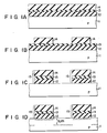
- silicon oxide film (SiO2) 12 with 3 to 4 ⁇ m thickness is first formed on P-type silicon substrate 11. Then, silicon nitride film (Si3N4) 13 with the thickness of 3000 to 5000 ⁇ is formed on silicon oxide film 12, and resist layer 14 containing organic compound as the main component is formed to a thickness of 3 to 8 ⁇ m on silicon nitride film 13.
- resist film 14 is patterned by a photolithographic technique, and then an anisotropic etching process such as RIE process is effected with patterned resist film 14 used as a mask.
- an anisotropic etching process such as RIE process is effected with patterned resist film 14 used as a mask.
- silicon nitride film 13 and silicon oxide film 12 are selectively removed to expose a predetermined portion of the surface of substrate 11.
- an N-type impurity such as phosphorus (P) is ion-implanted with block layer 15, which is formed of the remaining resist layer 14, silicon nitride film 13 and silicon oxide film 12, used as a mask in order to form N-type wells and N-type embedded layers.
- the acceleration voltage in the ion-implantation process is so set that phosphorus can be introduced into the surface area of substrate 11 through block layer 15 as shown by marks x in Fig. 1D and into a portion deeper than the substrate surface area in the exposed predetermined portion.
- an acceleration voltage 1.5 to 2.5 MeV.
- the dose amount of phosphorus at the time of the ion-implantation is preferably set to approx. 3 x 10¹².
- a P-type impurity such as boron (B) is ionimplanted with block layer 15 used as a mask in order to form P-type wells.
- the acceleration voltage in the ion-implantation process is so set that introduction of boron into substrate 11, as shown by marks o in Fig. 1E, is prevented by block layer 15, and at the same time boron can be intoruduced into the substrate surface area in the exposed predetermined portion. It is preferably to ion-implant boron at an acceleration voltage of 80 to 120 KeV. In this condition, boron is not introduced into substrate 11 under block layer 15 and is introduced into substrate 11 in the predetermined portion to substantially the same depth as phosphorus doped into substrate 11 under block layer 15.
- the dose amount of boron at the time of the ion-implantation is preferably set to approx. 2 x 10¹².
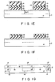
- a wet etching process is effected using a mixture of sulfuric acid solution and hydrogen peroxide solution to remove resist layer 14.
- silicon nitride film 13 is removed by a chemical vapor etching process, and then a wet etching process is effected using ammonium fluoride (NH4F) solution to remove silicon oxide film 12.
- a heat treatment is effected to diffuse phosphorus and boron which has been introduced in substrate 11. The heat treatment is effected for approx. three hours at a temperature of 1000 to 1200°C.
- the phosphorus and boron are diffused to form N-type wells 16, P-type wells 17 and N-type embedded layers 18 as shown in Fig. 1G.
- the impurity concentration of N-type wells 16 and P-type wells 17 is approx. 1 x 10¹⁶ to 1 x 10¹⁷/cm3
- the impurity concentration of N-type embedded layers 18 is approx. 1 x 10¹⁸ to 1 x 10¹⁹/cm3.
- the impurity concentration of N-type embedded layer 18 is set to be higher than that of N-type well 16. This is because phosphorus has been ion-implanted into that part of substrate 11 which corresponds to the N-type well through block layer 15 and phosphorus has been directly ion-implanted into that portion of substrate 11 which corresponds to N-type embedded layer 18. In other words, the amount of phosphorus introduced into substrate 11 under block layer 15 is reduced by the presence of block layer 15.
- N-type embedded layer 18 having a higher impurity concentration than N-type well 16, can be formed by effecting a single ion-implantation process.
- P-channel MOS transistors Tp and PNP transistors Qp are respectively formed in N-type wells 16 and P-type wells 17 by using the normal MOS process and bipolar process which are well known in the art.
- P-type layers 19 and 20 act as the source and drain of transistor T p
- metal film 22 formed on insulation film 21 which is formed on N-type well 16 acts as a gate electrode thereof.
- P-type well 17 acts as a collector of PNP transistor Qp
- N-type layer 23 and P-type layer 24 respectively act as the base and emitter thereof.
- boron is ion-implanted as the P-type impurity after phosphorus of N-type impurity has been ion-implanted.
- ion-implant boron first and then ion-implant phosphorus.
- boron fluoride (BF2) instead of boron and arsenide instead of phosphorus.
- CMOS semiconductor device it is possible to form an N-channel MOS transistor instead of PNP transistor Qp in P-type well 17.
- the semiconductor device shown in Fig. 1H is modified to a CMOS semiconductor device.
- Fig. 2 is a cross sectional view of a semiconductor device in which a plurality of P-type wells 17 are formed in substrate 11, and PNP transistors Qp and N-channel MOS transistors TN are selectively formed in P-type wells 17.
- N-channel MOS transistor TN of Fig. 2 N-type layers 25 and 26 act as the source and drain and metal film 28 formed on insulation film 27 which is in turn formed on P-type well 17 acts as a gate electrode.
- the semiconductor device of Fig. 2 is a Bi-CMOS semiconductor device.
- block layer 15 is used as a common mask for ion-implantation processes of N- and P-type impurities. Therefore, the patterning process necessary for forming the mask is effected only once. Further, N-type well 16 and high impurity N-type embedded layer 18 can be formed by a single ion-implantation process without forming an epitaxial layer. Thus, a twin well type semiconductor device can be formed by a simple manufacturing process, keeping the manufacturing cost low and enhancing the manufacturing yield.
Landscapes
- Metal-Oxide And Bipolar Metal-Oxide Semiconductor Integrated Circuits (AREA)
- Element Separation (AREA)
- Bipolar Transistors (AREA)
Applications Claiming Priority (2)
| Application Number | Priority Date | Filing Date | Title |
|---|---|---|---|
| JP62318649A JPH01161752A (ja) | 1987-12-18 | 1987-12-18 | 半導体装置製造方法 |
| JP318649/87 | 1987-12-18 |
Publications (2)
| Publication Number | Publication Date |
|---|---|
| EP0320977A2 true EP0320977A2 (de) | 1989-06-21 |
| EP0320977A3 EP0320977A3 (de) | 1990-02-14 |
Family
ID=18101490
Family Applications (1)
| Application Number | Title | Priority Date | Filing Date |
|---|---|---|---|
| EP88121131A Withdrawn EP0320977A3 (de) | 1987-12-18 | 1988-12-16 | Verfahren zum Herstellen von Halbleiteranordnungen mit Doppelwannen |
Country Status (4)
| Country | Link |
|---|---|
| US (1) | US4931406A (de) |
| EP (1) | EP0320977A3 (de) |
| JP (1) | JPH01161752A (de) |
| KR (1) | KR910009034B1 (de) |
Cited By (1)
| Publication number | Priority date | Publication date | Assignee | Title |
|---|---|---|---|---|
| EP0550021A3 (en) * | 1991-12-30 | 1996-12-27 | Texas Instruments Inc | Self-aligned single-mask cmos/bicmos twin-well formation with flat surface topography |
Families Citing this family (11)
| Publication number | Priority date | Publication date | Assignee | Title |
|---|---|---|---|---|
| JP2611461B2 (ja) * | 1989-12-20 | 1997-05-21 | 日本電気株式会社 | 半導体集積回路の製造方法 |
| KR940009997B1 (ko) * | 1991-05-03 | 1994-10-19 | 현대전자산업 주식회사 | Cmos의 단차없는 두개의 웰 제조방법 |
| US5242841A (en) * | 1992-03-25 | 1993-09-07 | Texas Instruments Incorporated | Method of making LDMOS transistor with self-aligned source/backgate and photo-aligned gate |
| US5369043A (en) * | 1992-12-25 | 1994-11-29 | Nippon Telegraph And Telephone Corporation | Semiconductor circuit device and method for production thereof |
| JP3031117B2 (ja) * | 1993-06-02 | 2000-04-10 | 日産自動車株式会社 | 半導体装置の製造方法 |
| US5411899A (en) * | 1993-10-13 | 1995-05-02 | At&T Corp. | Transistor fabrication of a twin tub using angled implant |
| KR0179794B1 (ko) * | 1995-12-28 | 1999-03-20 | 문정환 | 반도체 소자의 웰 형성방법 |
| KR100189739B1 (ko) * | 1996-05-02 | 1999-06-01 | 구본준 | 반도체 기판에 삼중웰을 형성하는 방법 |
| DE69735323T2 (de) * | 1996-09-05 | 2006-11-02 | Matsushita Electric Industrial Co., Ltd., Kadoma | Halbleiteranordnung und deren Herstellungsverfahren |
| US6107672A (en) * | 1997-09-04 | 2000-08-22 | Matsushita Electronics Corporation | Semiconductor device having a plurality of buried wells |
| JPH11288896A (ja) | 1998-04-03 | 1999-10-19 | Mitsubishi Electric Corp | 半導体装置の製造方法及び半導体装置 |
Family Cites Families (13)
| Publication number | Priority date | Publication date | Assignee | Title |
|---|---|---|---|---|
| US3897274A (en) * | 1971-06-01 | 1975-07-29 | Texas Instruments Inc | Method of fabricating dielectrically isolated semiconductor structures |
| US4306916A (en) * | 1979-09-20 | 1981-12-22 | American Microsystems, Inc. | CMOS P-Well selective implant method |
| NL186662C (nl) * | 1980-04-29 | 1992-03-16 | Philips Nv | Werkwijze ter vervaardiging van een halfgeleiderinrichting. |
| US4346512A (en) * | 1980-05-05 | 1982-08-31 | Raytheon Company | Integrated circuit manufacturing method |
| US4684971A (en) * | 1981-03-13 | 1987-08-04 | American Telephone And Telegraph Company, At&T Bell Laboratories | Ion implanted CMOS devices |
| NL188923C (nl) * | 1983-07-05 | 1992-11-02 | Philips Nv | Werkwijze ter vervaardiging van een halfgeleiderinrichting. |
| US4574467A (en) * | 1983-08-31 | 1986-03-11 | Solid State Scientific, Inc. | N- well CMOS process on a P substrate with double field guard rings and a PMOS buried channel |
| US4710477A (en) * | 1983-09-12 | 1987-12-01 | Hughes Aircraft Company | Method for forming latch-up immune, multiple retrograde well high density CMOS FET |
| US4637125A (en) * | 1983-09-22 | 1987-01-20 | Kabushiki Kaisha Toshiba | Method for making a semiconductor integrated device including bipolar transistor and CMOS transistor |
| US4554726A (en) * | 1984-04-17 | 1985-11-26 | At&T Bell Laboratories | CMOS Integrated circuit technology utilizing dual implantation of slow and fast diffusing donor ions to form the n-well |
| JPS61242064A (ja) * | 1985-04-19 | 1986-10-28 | Toshiba Corp | 相補型半導体装置の製造方法 |
| US4717683A (en) * | 1986-09-23 | 1988-01-05 | Motorola Inc. | CMOS process |
| JPH0797606B2 (ja) * | 1986-10-22 | 1995-10-18 | 株式会社日立製作所 | 半導体集積回路装置の製造方法 |
-
1987
- 1987-12-18 JP JP62318649A patent/JPH01161752A/ja active Pending
-
1988
- 1988-12-09 US US07/282,138 patent/US4931406A/en not_active Expired - Fee Related
- 1988-12-16 EP EP88121131A patent/EP0320977A3/de not_active Withdrawn
- 1988-12-17 KR KR1019880016872A patent/KR910009034B1/ko not_active Expired
Cited By (1)
| Publication number | Priority date | Publication date | Assignee | Title |
|---|---|---|---|---|
| EP0550021A3 (en) * | 1991-12-30 | 1996-12-27 | Texas Instruments Inc | Self-aligned single-mask cmos/bicmos twin-well formation with flat surface topography |
Also Published As
| Publication number | Publication date |
|---|---|
| JPH01161752A (ja) | 1989-06-26 |
| KR890011097A (ko) | 1989-08-12 |
| KR910009034B1 (ko) | 1991-10-28 |
| US4931406A (en) | 1990-06-05 |
| EP0320977A3 (de) | 1990-02-14 |
Similar Documents
| Publication | Publication Date | Title |
|---|---|---|
| US4764482A (en) | Method of fabricating an integrated circuit containing bipolar and MOS transistors | |
| US4434543A (en) | Process for producing adjacent tubs implanted with dopant ions in the manufacture of LSI complementary MOS field effect transistors | |
| EP0320977A2 (de) | Verfahren zum Herstellen von Halbleiteranordnungen mit Doppelwannen | |
| US5413944A (en) | Twin tub CMOS process | |
| KR930009807B1 (ko) | 바이폴라트랜지스터와 그 제조방법 | |
| JPH0775243B2 (ja) | 半導体装置の製造方法 | |
| KR930010094B1 (ko) | 반도체장치와 그 제조방법 | |
| JP2003031679A (ja) | 半導体装置の製造方法 | |
| JP2002016158A (ja) | 半導体装置の製造方法 | |
| JP2575876B2 (ja) | 半導体装置 | |
| KR100465606B1 (ko) | 반도체소자의 삼중웰 제조방법 | |
| KR100259586B1 (ko) | 반도체장치 제조방법 | |
| JP2633525B2 (ja) | 半導体装置の製造方法 | |
| JPH056961A (ja) | 半導体装置の製造方法 | |
| JPH02189965A (ja) | 半導体装置の製造方法 | |
| JP2982393B2 (ja) | 半導体装置の製造方法 | |
| JP3309529B2 (ja) | 半導体装置の製造方法 | |
| JP3134778B2 (ja) | 半導体装置の製造方法 | |
| JPH11340335A (ja) | 半導体装置の製造方法 | |
| JPH04346263A (ja) | Bi−CMOS半導体装置の製造方法 | |
| JPH04259254A (ja) | Cmos半導体装置の製造方法 | |
| JPH0745711A (ja) | 半導体装置の製造方法 | |
| JPH09129747A (ja) | 半導体装置の製造方法 | |
| JPH07135256A (ja) | 半導体装置の製造方法 | |
| JPH0638474B2 (ja) | 半導体装置の製造方法 |
Legal Events
| Date | Code | Title | Description |
|---|---|---|---|
| PUAI | Public reference made under article 153(3) epc to a published international application that has entered the european phase |
Free format text: ORIGINAL CODE: 0009012 |
|
| 17P | Request for examination filed |
Effective date: 19881216 |
|
| AK | Designated contracting states |
Kind code of ref document: A2 Designated state(s): DE FR GB IT |
|
| PUAL | Search report despatched |
Free format text: ORIGINAL CODE: 0009013 |
|
| RHK1 | Main classification (correction) |
Ipc: H01L 21/82 |
|
| AK | Designated contracting states |
Kind code of ref document: A3 Designated state(s): DE FR GB IT |
|
| 17Q | First examination report despatched |
Effective date: 19920515 |
|
| STAA | Information on the status of an ep patent application or granted ep patent |
Free format text: STATUS: THE APPLICATION IS DEEMED TO BE WITHDRAWN |
|
| 18D | Application deemed to be withdrawn |
Effective date: 19930320 |