EP0337775B1 - Elektronische Vorrichtung - Google Patents
Elektronische Vorrichtung Download PDFInfo
- Publication number
- EP0337775B1 EP0337775B1 EP89303645A EP89303645A EP0337775B1 EP 0337775 B1 EP0337775 B1 EP 0337775B1 EP 89303645 A EP89303645 A EP 89303645A EP 89303645 A EP89303645 A EP 89303645A EP 0337775 B1 EP0337775 B1 EP 0337775B1
- Authority
- EP
- European Patent Office
- Prior art keywords
- region
- integrated circuit
- conductors
- substrate
- area
- Prior art date
- Legal status (The legal status is an assumption and is not a legal conclusion. Google has not performed a legal analysis and makes no representation as to the accuracy of the status listed.)
- Expired - Lifetime
Links
- 239000004020 conductor Substances 0.000 claims description 107
- 239000000758 substrate Substances 0.000 claims description 89
- VYPSYNLAJGMNEJ-UHFFFAOYSA-N Silicium dioxide Chemical compound O=[Si]=O VYPSYNLAJGMNEJ-UHFFFAOYSA-N 0.000 claims description 16
- 229910052681 coesite Inorganic materials 0.000 claims description 8
- 229910052906 cristobalite Inorganic materials 0.000 claims description 8
- 239000000377 silicon dioxide Substances 0.000 claims description 8
- 229910052682 stishovite Inorganic materials 0.000 claims description 8
- 229910052905 tridymite Inorganic materials 0.000 claims description 8
- 229910004205 SiNX Inorganic materials 0.000 claims description 7
- 229920005989 resin Polymers 0.000 claims description 6
- 239000011347 resin Substances 0.000 claims description 6
- 238000007789 sealing Methods 0.000 claims description 5
- 238000009413 insulation Methods 0.000 description 62
- 239000011521 glass Substances 0.000 description 54
- 239000004973 liquid crystal related substance Substances 0.000 description 40
- 239000010408 film Substances 0.000 description 20
- 238000000034 method Methods 0.000 description 16
- 230000002950 deficient Effects 0.000 description 11
- 230000008569 process Effects 0.000 description 10
- 238000004519 manufacturing process Methods 0.000 description 9
- 238000000206 photolithography Methods 0.000 description 9
- 230000000694 effects Effects 0.000 description 6
- 239000000463 material Substances 0.000 description 5
- 229920002120 photoresistant polymer Polymers 0.000 description 4
- 229920003002 synthetic resin Polymers 0.000 description 4
- 239000000057 synthetic resin Substances 0.000 description 4
- 239000010409 thin film Substances 0.000 description 4
- RYGMFSIKBFXOCR-UHFFFAOYSA-N Copper Chemical compound [Cu] RYGMFSIKBFXOCR-UHFFFAOYSA-N 0.000 description 3
- 230000002411 adverse Effects 0.000 description 3
- 230000015572 biosynthetic process Effects 0.000 description 3
- 238000005229 chemical vapour deposition Methods 0.000 description 3
- PXHVJJICTQNCMI-UHFFFAOYSA-N nickel Substances [Ni] PXHVJJICTQNCMI-UHFFFAOYSA-N 0.000 description 3
- 238000012545 processing Methods 0.000 description 3
- 238000004544 sputter deposition Methods 0.000 description 3
- 238000009833 condensation Methods 0.000 description 2
- 230000005494 condensation Effects 0.000 description 2
- 239000011889 copper foil Substances 0.000 description 2
- 238000010030 laminating Methods 0.000 description 2
- 239000002184 metal Substances 0.000 description 2
- 229910052751 metal Inorganic materials 0.000 description 2
- 238000001259 photo etching Methods 0.000 description 2
- ATJFFYVFTNAWJD-UHFFFAOYSA-N Tin Chemical compound [Sn] ATJFFYVFTNAWJD-UHFFFAOYSA-N 0.000 description 1
- 230000002159 abnormal effect Effects 0.000 description 1
- 239000000969 carrier Substances 0.000 description 1
- 229910052802 copper Inorganic materials 0.000 description 1
- 239000010949 copper Substances 0.000 description 1
- 238000005260 corrosion Methods 0.000 description 1
- 230000007797 corrosion Effects 0.000 description 1
- 238000005520 cutting process Methods 0.000 description 1
- 238000007598 dipping method Methods 0.000 description 1
- 238000001312 dry etching Methods 0.000 description 1
- 238000005401 electroluminescence Methods 0.000 description 1
- 238000009713 electroplating Methods 0.000 description 1
- 230000002708 enhancing effect Effects 0.000 description 1
- PCHJSUWPFVWCPO-UHFFFAOYSA-N gold Chemical compound [Au] PCHJSUWPFVWCPO-UHFFFAOYSA-N 0.000 description 1
- 239000010931 gold Substances 0.000 description 1
- 229910052737 gold Inorganic materials 0.000 description 1
- AMGQUBHHOARCQH-UHFFFAOYSA-N indium;oxotin Chemical compound [In].[Sn]=O AMGQUBHHOARCQH-UHFFFAOYSA-N 0.000 description 1
- 239000011159 matrix material Substances 0.000 description 1
- 230000004048 modification Effects 0.000 description 1
- 238000012986 modification Methods 0.000 description 1
- 229910052759 nickel Inorganic materials 0.000 description 1
- 230000003287 optical effect Effects 0.000 description 1
- 239000002245 particle Substances 0.000 description 1
- 238000000059 patterning Methods 0.000 description 1
- 230000002093 peripheral effect Effects 0.000 description 1
- 229920001721 polyimide Polymers 0.000 description 1
- 230000001681 protective effect Effects 0.000 description 1
- 230000009467 reduction Effects 0.000 description 1
- 239000003566 sealing material Substances 0.000 description 1
- 229910000679 solder Inorganic materials 0.000 description 1
- 239000002904 solvent Substances 0.000 description 1
- 230000007480 spreading Effects 0.000 description 1
- 238000003892 spreading Methods 0.000 description 1
- 238000001039 wet etching Methods 0.000 description 1
Images



Classifications
-
- G—PHYSICS
- G02—OPTICS
- G02F—OPTICAL DEVICES OR ARRANGEMENTS FOR THE CONTROL OF LIGHT BY MODIFICATION OF THE OPTICAL PROPERTIES OF THE MEDIA OF THE ELEMENTS INVOLVED THEREIN; NON-LINEAR OPTICS; FREQUENCY-CHANGING OF LIGHT; OPTICAL LOGIC ELEMENTS; OPTICAL ANALOGUE/DIGITAL CONVERTERS
- G02F1/00—Devices or arrangements for the control of the intensity, colour, phase, polarisation or direction of light arriving from an independent light source, e.g. switching, gating or modulating; Non-linear optics
- G02F1/01—Devices or arrangements for the control of the intensity, colour, phase, polarisation or direction of light arriving from an independent light source, e.g. switching, gating or modulating; Non-linear optics for the control of the intensity, phase, polarisation or colour
- G02F1/13—Devices or arrangements for the control of the intensity, colour, phase, polarisation or direction of light arriving from an independent light source, e.g. switching, gating or modulating; Non-linear optics for the control of the intensity, phase, polarisation or colour based on liquid crystals, e.g. single liquid crystal display cells
- G02F1/133—Constructional arrangements; Operation of liquid crystal cells; Circuit arrangements
- G02F1/1333—Constructional arrangements; Manufacturing methods
- G02F1/1345—Conductors connecting electrodes to cell terminals
- G02F1/13452—Conductors connecting driver circuitry and terminals of panels
-
- G—PHYSICS
- G02—OPTICS
- G02F—OPTICAL DEVICES OR ARRANGEMENTS FOR THE CONTROL OF LIGHT BY MODIFICATION OF THE OPTICAL PROPERTIES OF THE MEDIA OF THE ELEMENTS INVOLVED THEREIN; NON-LINEAR OPTICS; FREQUENCY-CHANGING OF LIGHT; OPTICAL LOGIC ELEMENTS; OPTICAL ANALOGUE/DIGITAL CONVERTERS
- G02F1/00—Devices or arrangements for the control of the intensity, colour, phase, polarisation or direction of light arriving from an independent light source, e.g. switching, gating or modulating; Non-linear optics
- G02F1/01—Devices or arrangements for the control of the intensity, colour, phase, polarisation or direction of light arriving from an independent light source, e.g. switching, gating or modulating; Non-linear optics for the control of the intensity, phase, polarisation or colour
- G02F1/13—Devices or arrangements for the control of the intensity, colour, phase, polarisation or direction of light arriving from an independent light source, e.g. switching, gating or modulating; Non-linear optics for the control of the intensity, phase, polarisation or colour based on liquid crystals, e.g. single liquid crystal display cells
- G02F1/133—Constructional arrangements; Operation of liquid crystal cells; Circuit arrangements
- G02F1/1333—Constructional arrangements; Manufacturing methods
- G02F1/1345—Conductors connecting electrodes to cell terminals
Definitions
- the present invention relates to display apparatus such as a liquid crystal display device, and more particularly possessing a structure in which an integrated circuit is connected to, for example, a glass substrate of a display panel.
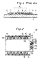
- FIG. 1 is a sectional view showing the structure near a tape carrier 6 of a liquid crystal display device in a typical prior art.
- Two glass substrates composing the liquid crystal panel are overlapped with an offset. Therefore, one glass substrate 2 possesses a region not overlapping with the other glass substrate. In this region, the tape carrier 6, to which an integrated circuit (not shown) or the like for driving the liquid crystal is attached, is connected. In the overlapping region of the two glass substrates, liquid crystal material or the like is sealed between the two substrates, so as to effect liquid crystal display in this region.
- a common conductor 4 for carrying an input signal is disposed on the surface of the glass substrate 2.
- an input signal conductor 3 and a connecting conductor 7 are formed on the surface of the tape carrier 6 confronting the glass substrate 2. This connecting conductor 7 is connected to the common conductor 4 by way of an anisotropic conductive film 5.
- the input signal conductor 3 on the tape carrier 6 and the common conductor 4 formed on the glass substrate 2 cross over to form a multilayer conductor structure.
- a resist 1 such as an electrically insulating resin is applied on the input signal conductor 3.
- the input signal conductor 3 on the tape carrier 6 and the common conductor 4 on the glass substrate 2 are insulated from each other.
- the tape carrier 6 is deformed in the region indicated by reference A1.
- Such deformation of the tape carrier 6 is considered to be caused due to the relatively large thickness of the resist 1, and the difference between the thermal expansion coefficients of the resist 1 and the tape carrier 6.
- a stress is caused in the connection part of the common conductor 4 and the connecting conductor 7, which may result in defective connection or the like.
- the conductor from the tape carrier 6 to the display region is formed on the surface of the glass substrate 2.
- the spacing between conductors is too narrow, due to dew condensation of moisture defective insulation occurs, and hence there is a limit to the miniaturization of wiring conductors.
- defective insulation due to foreign deposit may also take place.
- the above technical problems are not sclved.
- positioning of high precision is required in connecting the integrated circuit to the glass substrate. That is, where the conductor interval is narrow in the connecting part, a slight dislocation may give rise to short-circuit or leak between the connecting electrode of the integrated circuit and the conductor adjacent to the connecting position of the glass substrate.
- this conductive paste may be spread widely unexpectedly when connecting, which may also lead to short-circuit or leak between the adjoining conductors.
- the invention provides display apparatus comprising:
- connection electrodes may be aligned in lines parallel to the direction in which the conductors extend from said first region to said second region.
- a sealing resin fills the gap between said integrated circuit component and said first substrate.
- the invention provides display apparatus comprising:
- the insulating layer covers substantially the whole of each of said conductors.
- the insulating layer in said area is confined to covering portions of said conductors which lie adjacent the connection electrodes of others of said conductors.
- connection electrodes may be aligned in lines parallel to the direction in which the conductors extend from said first region to said second region.
- the electrically insulating layer may comprise SiO 2 or SiN x .
- a thin layer of this material may be formed preferably by the sputtering method, the CVD method, or another thin layer forming technique. The thin layer may then be patterned using the photolithographic technique.
- the electrically insulating layer is selectively formed in the region (hereafter "the connection region") other than the display panel-forming region of the substrate, for example by photolithography.
- the bonding electrodes of the integrated circuit component are connected to the connection electrodes of the conductors on the substrate in the bond region of the conductors free from the electrically insulating layer.
- the insulation performance between the conductors in the connection region is enhanced by the electrically insulating layer for forming the display panel, defective insulation between the conductors may be prevented without complicating the manufacturing process.
- the display apparatus may be composed by forming an electrically insulating layer by photolithography on the electrically insulating substrate on which the conductors are formed. At this time, since the electrically insulating layer is selectively formed in the connection region the insulation between the wiring conductors may be enhanced, so that fine and high density formation of the conductors may be realized.
- the electrically insulating layer in the non-bonding region between the integrated circuit component and the substrate, it is possible to provide insulation while eliminating the adverse effects on the connection due to the great thickness of the resist as mentioned in relation to the prior art. Furthermore, in the forming process of the electrically insulating layer when composing the display apparatus, the electrically insulating layer can be formed in the region other than the display panel-forming region, so that the manufacturing process of the display apparatus may be simplified.
- the integrated circuit By forming the electrically insulating layer selectively in the connection region, connecting the integrated circuit to the substrate, and injecting an electrically insulating synthetic resin between the integrated circuit and the substrate, the integrated circuit can be connected firmly to the circuit substrate, without worsening the insulating performance between the conductors even when the adhesion between the electrically insulating layer and the synthetic resin is weak.
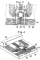
- FIG. 2 is a plan view showing the entire structure of a liquid crystal display device 30.
- the liquid crystal display device 30 is composed by laminating two glass substrates 12, 22 as a pair of substrates. These two glass substrates 12, 22 are overlapped with an offset, and possess regions not overlapping with each other. In these regions, plural integrated circuits 23 for driving the liquid crystal are connected individually through tape carriers 16.
- the tape carrier 16 is intended to connect the integrated circuit 23 electrically to the glass substrates 12, 22, and it is made of an elastic film. As mentioned later, in the display region 31, intervening between the two glass substrates 12, 22, there are a colour filter, transparent electrodes 18,28, transparent insulation films 11a,21 made of electrically insulating film, orientation films 19,29 and liquid crystal 27 whereby the liquid crystal display is realized.
- An input signal is supplied from a common conductor 14 for input signal to the integrated circuit 23 through a tape carrier 16.
- This common conductor 14 for input signal is formed on the surface of the glass substrate 12.
- the output signal from the integrated circuit 23 is applied to electrode 18 through the tape carrier 16.
- the electrode 18 is disposed in the region on the glass substrate 12 from the tape carrier 16 to the display region 31. Such structure is similar in the region not overlapping with the glass substrate 12 of the glass substrate 22.
- the electrodes 18, 28 from the tape carrier 16 compose a matrix by extending longitudinally and laterally in the display region 31, and a two-dimensional display is achieved on the display region 31.
- a transparent insulation layer is formed, as mentioned later, not only in the display region 31 (as indicated by reference 11a in FIG.5), but also in the overlapping region A2 (as indicated by reference 11) with the tape carrier 16 and the exposed region A3 (as 11a) of the electrodes 18, 28.
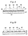
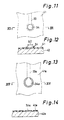
- FIG. 3 is a plan view showing the structure near the tape carrier 16 of the liquid crystal display device 30, and FIG. 4 is a perspective view showing this structure.
- the electrode 18 and common conductor 14 for input signal are formed on the surface of the glass substrate 12.
- the common conductor 14 for input signal and electrode 18 formed on the glass substrate 12 are made of, for example, ITO (indium-tin oxide) or other metal film.
- transparent insulation layers are formed.
- the transparent insulation layers are, for example, SiO 2 and SiN x , and are formed by sputtering method, CVD method or the like in the forming process of liquid crystal panel 20, and fine patterns may be easily formed by photoetching or photolithography.
- this transparent insulation layer On the entire surface of the glass substrate 12, on which the electrode 18 and common conductor 14 for input signal are formed, a thin layer of SiO 2 or SiN 2 is formed in a layer thickness of, for example, 3000 ⁇ . Furthermore, a photosetting photo resist is applied on the entire surface, and it is irradiated with light through a mask with desired pattern. Dipping in a solvent in this state, the photo resist which is not cured is dissolved and removed. Moreover, by the wet etching or dry etching method, the portion of SiO 2 or SiN x exposed by the removal of the photo resist is removed. As a result, the SiO 2 or SiN x layer is formed in a pattern, and the remaining photo resist is removed. A transparent insulation layer is formed later.
- an input signal conductor 13 is formed on the surface of the tape carrier 16 confronting the glass substrate 12, and the input signal conductor 13 and the corresponding common conductor 14 for input signal are electrically connected individually by means of an anisotropic conductive film 15 (see FIG. 3).
- the tape carrier 16 is composed of, for example, an organic resin film small in thermal expansion coefficient.
- the input signal conductor 13 and connecting conductor 17 formed on the tape carrier 16 are, for example, made of copper foil, tin foil or tin-plated copper foil, and they can be arranged finely and at high density by applying the techniques of thin film pattern processing or the like.
- the anisotropic conductive film 15 is composed of, for example, a sheet of about 25 ⁇ m in thickness having Ni (nickel particles) of 5 to 20 ⁇ m in diameter dispersed therein, and the heated and compressed portion becomes conductive in the compressing direction. This anisotropic conductive film 15 also possesses the function for mechanically connecting the tape carrier 16 and the glass substrate 12.
- the input signal conductor 13 and the common conductor 14 for input signal are not connected, and a multilayer structure is built up.
- the electrode 18 is exposed.
- the transparent insulation layer 11 formed in the region A2 by the transparent insulation layer 11 formed in the region A2, the insulation of the input signal conductor 13 and the common conductor 14 for input signal is achieved.
- the transparent insulation layer 11a formed in the region A3 defective insulation between electrodes 18 due to foreign deposit may be prevented.
- FIG. 5 is a sectional view of the liquid crystal display device 30, and FIG. 6 is a sectional view near the tape carrier 16 showing the liquid crystal display device 30 cut off along the common conductor 14 for input signal.
- the integrated circuit 23 for driving the liquid crystal is mounted on the tape carrier 16.
- An output wire 24 from this integrated circuit 23 is bonded to an inner lead by bumps 25, and is individually connected to the input signal conductor 13, and to electrode 18 by way of anisotropic conductive film 15, solder or other connecting material.
- the display panel 20 positioned at the left side in FIG. 5 is composed by laminating the glass substrate 12 on which a segment electrode 18 is formed, and the glass substrate 22 on which a common electrode 28 is formed.
- colour filter 32 and electrode 18 are formed, and a transparent insulation layer lla is formed on this electrode 18.
- an alignment layer 19 is formed on the transparent insulation layer lla corresponding to the display region 31 of the display panel 20, an alignment layer 19 is formed.
- electrode 28 transparent insulation layer 21 and orientation film 29 are formed.
- the glass substrate 12 and glass substrate 22 are fixed by way of sealing material 26, and a liquid crystal intervenes between the alignment layer 19 and the alignment layer 29.
- a voltage is selectively applied to each picture element between the electrodes 18, 28 by the signal delivered from the integrated circuit 23 to the electrode 18, and the signal led out to the electrode 28, and the optical characteristic of the liquid crystal 27 varies, so that the image display is realized.
- the structure near the connecting part of the tape carrier 16 and glass substrate 12 is described in detail.
- the transparent insulation layer 11 is formed, in the same process as in the transparent insulation layer 11a, in the region A2, A3 as mentioned above.
- the region A2 is an area in which the common conductor 14 for input signal and input signal conductor 13 cross over to build up a multilayer conductor structure, and usually in this region A2 a short-circuit between conductors is likely to occur.
- the connecting conductor 17 of the tape carrier 16 and the electrode 18, and the input signal conductor 13 of the tape carrier 16 and the common conductor 14 for input signal are electrically and mechanically connected with each other respectively, by way of the anisotropic conductive film 15. In such a connecting position, the transparent insulation layer 11 is not formed.
- the transparent insulation layer 11 is formed in the region A2
- this transparent insulation layer 11 is a thin film, its thickness is not so great as that of the resist. What is more, since it is not directly adhered to the tape carrier 16, it is free from adverse effects of difference in the thermal expansion coefficient between the tape carrier 16 and the resist. Accordingly, the tape carrier 16 is not deformed in the region A2. Therefore, since stress is not generated in the connecting portion of the input signal conductor 13 and common conductor 14 for input signal, adverse effects on connection are eliminated, and the reliability of connection is enhanced. At this time, the transparent insulation layer 11 is a thin film, and the yield in the connecting process by the anisotropic conductive film 15 is enhanced, so that the cost of the entire apparatus may be lowered at the same time.
- the transparent insulation layer 11 since the transparent insulation layer 11 is formed, the insulation between the adjoining electrodes 18 is improved, and defective insulation between the electrodes 18 due to dew condensation of moisture may be prevented. At the same time, defective insulation due to foreign deposit is prevented, so that fine patterning and high density of the electrodes 18 may be achieved at the same time. Besides, since such transparent electrode insulation layers 11 can be formed in the fabrication process of the display panel 20, these effects will be realized without complicating the manufacturing process.
- the transparent insulation layer 11 is formed in the region A2 and the region A3, but it is also possible to form the transparent insulation layer 11 either in the region A2 or A3, or the transparent insulation layer 11 may be also formed in part of such regions or in the portion other than such regions. In such a case, since the transparent insulation layer 11 is patterned at high density by photolithography, the transparent insulation layer 11 may be selectively formed in a desired region, for example, in the region where the defective insulation of the electrode 18 is likely to occur. Or, when the tape carrier is connected to an ordinary printed circuit board comprising common conductor for input signal and this tape carrier is connected to the glass substrate, the transparent insulation layer 11 is preferably formed on the electrode extending from the tape carrier to the display region.
- FIG. 7 is a plan view showing the connection structure of an integrated circuit 43 to a glass substrate 42 in a liquid crystal display device in one embodiment of the invention
- FIG. 8 is a sectional view seen from cut-off line VIII-VIII of FIG. 7
- FIG. 9 is a sectional view seen from cut-off line IX-IX of FIG. 7
- FIG. 10 is a sectional view seen from cut-off line X-X of FIG. 7.
- the integrated circuit 43 is directly connected to the region not overlapping between one glass substrate 42 and the other glass substrate in the liquid crystal display device. In the other glass substrate, similarly, an integrated circuit may be connected.
- output electrode 34, input electrode 35 and output conductor 33 are formed, for example, in the same process together with the picture element electrode or scanning electrode in the liquid crystal display device.
- Such electrodes are selectively formed by, for example, photolithography, and are composed of ITO or other metal thin film.
- a transparent insulation film 41 is formed as an electrically insulating film.
- This transparent insulation layer 41 is, the same as in the foregoing structure, for example, SiO 2 or SiN x , and is formed in a film by sputtering method, CVD method or the like, and is patterned by photolithography. As shown in FIGS. 8 to 10, the transparent insulation layer 41 is not formed in the regions B1, B2, in which connections are made to the input electrode 35, output electrode 34 and input terminal 36.
- the integrated circuit 43 has a function for driving the liquid crystal display device, and a bump electrode 37 is formed in order to exchange signals with the outside.
- This bump electrode 37 is formed by selectively applying a resist by photolithography, and applying copper by electroplating.
- a bump electrode made of gold may be formed in the same way as the fast bond of wire bonding method.
- This bump electrode 37 is electrically connected in the region B2 in which the output electrode 34 and the input electrode 35 are exposed.
- the integrated circuit 43 is electrically connected with the output electrode 34 and the input electrode 35 of the glass substrate 42.
- a conductive paste may be used, or they may be directly connected by compressing. Otherwise, without forming the bump electrode 37, the integrated circuit and the output electrode 34 and input electrode 35 of the glass substrate 42 may be connected by way of an anisotropic conductive film.
- FIG. 11 is a plan view showing the structure near the output electrode 34 in the connecting structure described above
- FIG. 12 is a sectional view seen from cut-off line XII-XII of FIG. 11.
- the transparent insulation layer 41 is formed, overlapping with the output electrode 34 partly in the peripheral part of the output electrode 34.
- the bump electrode 37 is connected to the exposed region B2 of the output electrode 34.
- FIG. 13 is a plan view showing the structure near the output electrode 34a of the liquid crystal display device in an embodiment of the invention
- FIG. 14 is a sectional view seen from cutoff line XIV-XIV of FIG. 13.
- This embodiment differs from the preceding structure in that the output electrode 34a and transparent insulation layer 41a do not overlap.
- the output conductor 33a which is manufactured in the same process as the output electrode 34a and is extending in the display region from the output electrode 34a is overlapping with the transparent insulation layer 41a. That is, the output conductor 33a is covered with the transparent insulation layer.
- a flexible printed circuit (FPC) or the like comprising the common conductor for input signal is connected to the region B1 of the input terminal 36, and an input signal from outside is given to this input terminal 36.
- This input signal is given to the integrated circuit 43 through input electrode 35 and bump electrode 37.
- various signal processings are done, and an output signal according to the input signal is delivered.
- This output signal is transmitted to the liquid crystal display unit from the bump electrode 37 of the integrated circuit 43 by way of the output electrode 34 and output conductor 33 on the glass substrate 42, so that a two-dimensional display is achieved.
- the transparent insulation layer 41 is formed on the surface of output conductor 33, the insulation between conductors is enhanced, and leak between conductors and corrosion of conductors may be prevented, and leak of bump electrode 37 and conductor 33 of the integrated circuit 43 due to defective positioning bf the integrated circuit 43 may be prevented.
- the process of forming the transparent insulation layer 41 is included in the manufacturing process of the liquid crystal panel, and it is conducted simultaneously with the formation of the transparent insulation film in the display region, so that the manufacturing process will not be complicated if the transparent insulation layer is formed in the region to be connected with the integrated circuit 43.
- the transparent insulation layer 41 is patterned by photo etching, the pattern positioning precision and pattern forming precision are excellent. Therefore, although fine conductors are formed on the glass substrate 42, arbitrary patterns can be formed depending on such fine conductor patterns. Hence, undesired short-circuit of conductors may be prevented.
- This transparent insulation layer 41 is, for example, SiO 2 or SiN x , but other materials may be equally employed as far as applicable to fine processing of photolithography or the like in the liquid crystal panel forming process.
- FIG. 15 and FIG. 16 are plan views showing the forming regions of output electrodes 34b, 34c, output conductors 33b, 33c, and transparent insulation layers 41b, 41c formed on the glass substrate opposite to the integrated circuit, according to further embodiments of the invention.
- a transparent insulation layer 41b is formed so as to cover the output conductor 33b along the output conductor 33b. According to this embodiment, since the transparent insulation layer 41b is patterned by photolithography, such fine patterns can be formed.
- FIG. 16 shows a case of forming the transparent insulation layer 41c so as to cover only the portion likely to cause short-circuit or leak with the output electrode 34c in the output conductor 33c existing near the output electrode 34c.
- liquid crystal display device liquid crystal display device
- this invention may be also embodied in other display devices, such as plasma display device, electroluminescence display device, and electrochromic display device.
Landscapes
- Physics & Mathematics (AREA)
- Nonlinear Science (AREA)
- Mathematical Physics (AREA)
- Chemical & Material Sciences (AREA)
- Crystallography & Structural Chemistry (AREA)
- General Physics & Mathematics (AREA)
- Optics & Photonics (AREA)
- Liquid Crystal (AREA)
- Devices For Indicating Variable Information By Combining Individual Elements (AREA)
Claims (8)
- Anzeigevorrichtung, mit:einem ersten elektrisch isolierendem Substrat (42), mit einem ersten Bereich, in dem durch ein darüberliegendes zweites elektrisch isolierendes Substrat ein Anzeigefeld gebildet ist, und einem zweiten Bereich, in dem die Substrate nicht übereinander liegen;Leitern (33b; 33c) auf dem ersten Substrat (42), die parallel von dem ersten Bereich, in dem sie einen Teil des Anzeigefeldes bilden, zu dem zweiten Bereich verlaufen, in dem sie in jeweiligen Verbindungselektroden (34b; 34c) enden;einem integrierten Schaltkreis (43), der das Anzeigefeld ansteuert, und der in dem zweiten Bereich Face-down auf dem ersten Substrat (42) angebracht ist, wobei der integrierte Schaltkreis (43) Bondelektroden (37) aufweist, die jeweils in dem Bereich unter dem integrierten Schaltkreis (43) elektrisch an die Verbindungselektroden (34b; 34c) angeschlossen sind;eine elektrisch isolierende Schicht (41b; 41c) über den Leitern (33b; 33c), die sich über den ersten und zweiten Bereich ausdehnt, wobei die elektrisch isolierende Schicht (41b; 41c) in dem durch den integrierten Schaltkreis (43) bedecken Bereich des zweiten Bereichs nur Abschnitte der Leiter (33b; 33c) bedeckt; undeinem Dichtharz (38), das die Lücke zwischen dem integrierten Schaltkreis (43) und dem ersten Substrat (42) im ganzen Bereich ausfüllt;wobei die Verbindungselektroden (34b; 34c) über den Bereich, in dem sie die Grundfläche und den Umfang belegen, regelmäßig angeordnet sind.
- Anzeigevorrichtung nach Anspruch 1, dadurch gekennzeichnet, daß die Verbindungselektroden (34b; 34c) in Linien parallel zu der Richtung ausgerichtet sind, in der die Leiter (33b; 33c) vom ersten Bereich zum zweiten Bereich verlaufen.
- Anzeigevorrichtung nach Anspruch 1 oder 2, dadurch gekennzeichnet, daß die Isolierschicht (41b) in dem Bereich im wesentlichen alle Leiter (33b) ganz bedeckt.
- Anzeigevorrichtung nach Anspruch 1 oder 2, dadurch gekennzeichnet, daß in dem Bereich die Isolierschicht (41b) die Abschnitte der Leiter (33c) nicht bedeckt, die neben den Verbindungselektroden (34c) anderer Leiter liegen.
- Anzeigevorrichtung, mit:einem ersten elektrisch isolierendem Substrat (42a), mit einem ersten Bereich, in dem durch ein darüberliegendes zweites elektrisch isolierendes Substrat ein Anzeigefeld gebildet wird, und einem zweiten Bereich, in dem die Substrate nicht übereinander liegen;Leitern (33a), die auf dem ersten Substrat (42a) gebildet sind und die parallel von dem ersten Bereich, in dem sie einem Teil des Anzeigefeldes bilden, zu dem zweiten Bereich verlaufen, in dem sie in jeweiligen Verbindungselektroden (34a) enden;einem integrierten Schaltkreis (43), der das Anzeigefeld ansteuert und der in dem zweiten Bereich Face-down auf dem ersten Substrat (42a) angebracht ist, wobei der integrierte Schaltkreis (43) Bondelektroden (37) aufweist, die jeweils in dem Bereich unter dem integrierten Schaltkreis (43) elektrisch an die Verbindungselektroden (34a) angeschlossen sind; undeine elektrisch isolierende Schicht (41a), die über den Leitern (33a) gebildet ist und sich über den ersten und zweiten Bereich einschließlich des Bereichs ausdehnt, der durch den integrierten Schaltkreis (43) bedeckt ist, wobei die Verbindungselektroden (34a) ausgeschlossen sind, an denen die elektrisch isolierende Schicht (41a) alle Verbindungselektroden (34a) ganz unbedeckt läßt, indem sie in einem Abstand um dem Umfang der Verbindungselektrode herum endet;wobei die Verbindungselektroden (34a) über den Bereich, in dem sie die Grundfläche und den Umfang belegen, regelmäßig angeordnet sind.
- Anzeigevorrichtung nach Anspruch 5, dadurch gekennzeichnet, daß die Verbindungselektroden (34a) in Linien parallel zur der Richtung ausgerichtet sind, in der die Leiter (33a) von dem ersten Bereich zum zweiten Bereich verlaufen.
- Anzeigevorrichtung nach Anspruch 5 oder 6, dadurch gekennzeichnet, daß ein Dichtharz (38) die Lücke zwischen dem integrierten Schaltkreis (43) und dem ersten Substrat (42a) ausfüllt.
- Anzeigevorrichtung nach einem der vorhergehenden Ansprüche, dadurch gekennzeichnet, daß die elektrisch isolierende Schicht (41) SiO2 oder SiNx enthält.
Applications Claiming Priority (2)
| Application Number | Priority Date | Filing Date | Title |
|---|---|---|---|
| JP91178/88 | 1988-04-12 | ||
| JP9117888 | 1988-04-12 |
Publications (3)
| Publication Number | Publication Date |
|---|---|
| EP0337775A2 EP0337775A2 (de) | 1989-10-18 |
| EP0337775A3 EP0337775A3 (en) | 1990-09-19 |
| EP0337775B1 true EP0337775B1 (de) | 1996-06-19 |
Family
ID=14019205
Family Applications (1)
| Application Number | Title | Priority Date | Filing Date |
|---|---|---|---|
| EP89303645A Expired - Lifetime EP0337775B1 (de) | 1988-04-12 | 1989-04-12 | Elektronische Vorrichtung |
Country Status (2)
| Country | Link |
|---|---|
| US (1) | US5016986A (de) |
| EP (1) | EP0337775B1 (de) |
Families Citing this family (29)
| Publication number | Priority date | Publication date | Assignee | Title |
|---|---|---|---|---|
| JPH03125444A (ja) * | 1989-10-09 | 1991-05-28 | Chisso Corp | 改良されたフィルムキャリヤー |
| JP2554769B2 (ja) * | 1990-05-16 | 1996-11-13 | 株式会社東芝 | 液晶表示装置 |
| EP0501413B1 (de) * | 1991-02-26 | 1996-10-02 | Rohm Co., Ltd. | Flache Anzeigevorrichtung |
| TW232065B (de) * | 1992-04-16 | 1994-10-11 | Sharp Kk | |
| DE9217429U1 (de) * | 1992-12-19 | 1994-01-27 | Schauer, Gernot, Dr., 89518 Heidenheim | Flüssigkristall-Anzeigevorrichtung |
| WO1994024604A1 (fr) * | 1993-04-09 | 1994-10-27 | Citizen Watch Co., Ltd. | Affichage a cristaux liquides |
| JP2878066B2 (ja) | 1993-05-24 | 1999-04-05 | シャープ株式会社 | 印刷回路基板の接続方法 |
| US7081938B1 (en) | 1993-12-03 | 2006-07-25 | Semiconductor Energy Laboratory Co., Ltd. | Electro-optical device and method for manufacturing the same |
| US5436745A (en) * | 1994-02-23 | 1995-07-25 | Ois Optical Imaging Systems, Inc. | Flex circuit board for liquid crystal display |
| US5654730A (en) * | 1994-08-16 | 1997-08-05 | Citizen Watch Co., Ltd. | Liquid crystal display device |
| US5841414A (en) * | 1994-08-16 | 1998-11-24 | Citizen Watch Co., Ltd. | Liquid crystal display device |
| TW344043B (en) * | 1994-10-21 | 1998-11-01 | Hitachi Ltd | Liquid crystal display device with reduced frame portion surrounding display area |
| US7195960B2 (en) * | 1996-06-28 | 2007-03-27 | Seiko Epson Corporation | Thin film transistor, manufacturing method thereof, and circuit and liquid crystal display device using the thin film transistor |
| JP3328157B2 (ja) * | 1997-03-06 | 2002-09-24 | シャープ株式会社 | 液晶表示装置 |
| JP3955376B2 (ja) * | 1997-05-13 | 2007-08-08 | セイコーエプソン株式会社 | 液晶表示パネルおよび液晶表示パネルの検査方法 |
| US6825836B1 (en) | 1998-05-16 | 2004-11-30 | Thomson Licensing S.A. | Bus arrangement for a driver of a matrix display |
| JP3904752B2 (ja) * | 1999-01-26 | 2007-04-11 | アルプス電気株式会社 | 反射型液晶表示装置およびその製造方法 |
| JP2000259091A (ja) * | 1999-03-04 | 2000-09-22 | Casio Comput Co Ltd | 表示パネル、フレキシブル配線基板及びそれらを備えた表示装置 |
| JP2001142090A (ja) * | 1999-11-11 | 2001-05-25 | Hitachi Ltd | 液晶表示装置 |
| JP2002311849A (ja) * | 2001-04-19 | 2002-10-25 | Seiko Epson Corp | 電極駆動装置及び電子機器 |
| JP2003121815A (ja) * | 2001-10-16 | 2003-04-23 | Nec Access Technica Ltd | Lcdの保持構造 |
| KR100654338B1 (ko) * | 2003-10-04 | 2006-12-07 | 삼성전자주식회사 | 테이프 배선 기판과 그를 이용한 반도체 칩 패키지 |
| KR100598032B1 (ko) * | 2003-12-03 | 2006-07-07 | 삼성전자주식회사 | 테이프 배선 기판, 그를 이용한 반도체 칩 패키지 및 그를이용한 디스플레이패널 어셈블리 |
| KR101075599B1 (ko) * | 2004-06-23 | 2011-10-20 | 삼성전자주식회사 | 표시장치 |
| US20070069701A1 (en) * | 2005-09-29 | 2007-03-29 | Dell Products L.P. | Low cost stability improvement for a linear voltage regulator |
| JP5353153B2 (ja) * | 2007-11-09 | 2013-11-27 | パナソニック株式会社 | 実装構造体 |
| KR101457335B1 (ko) * | 2008-01-21 | 2014-11-04 | 삼성전자주식회사 | 배선기판, 이를 갖는 테이프 패키지 및 표시장치 |
| CN102914921A (zh) * | 2012-10-11 | 2013-02-06 | 京东方科技集团股份有限公司 | 液晶面板上集成摄像头的方法、液晶面板及液晶显示装置 |
| KR20190083014A (ko) * | 2018-01-02 | 2019-07-11 | 삼성디스플레이 주식회사 | 표시 장치 |
Family Cites Families (12)
| Publication number | Priority date | Publication date | Assignee | Title |
|---|---|---|---|---|
| JPS5840728B2 (ja) * | 1978-08-23 | 1983-09-07 | 株式会社日立製作所 | 液晶表示装置 |
| JPS57164716A (en) * | 1981-04-03 | 1982-10-09 | Canon Inc | Electrooptical display device |
| NL8105922A (nl) * | 1981-12-31 | 1983-07-18 | Philips Nv | Werkwijze voor het partieel metalliseren van elektrisch geleidende niet-metallische patronen. |
| JPS5950444A (ja) * | 1982-09-16 | 1984-03-23 | Tokyo Ohka Kogyo Co Ltd | 微細加工用ホトマスク |
| JPS60130721A (ja) * | 1983-12-19 | 1985-07-12 | Citizen Watch Co Ltd | 液晶表示装置 |
| JPS60111068U (ja) * | 1983-12-28 | 1985-07-27 | アルプス電気株式会社 | フレキシブルプリント基板 |
| JPS60238817A (ja) * | 1984-05-12 | 1985-11-27 | Citizen Watch Co Ltd | 液晶表示装置 |
| JPS61123818A (ja) * | 1984-11-21 | 1986-06-11 | Hitachi Ltd | 液晶表示素子 |
| JPS61123868A (ja) * | 1984-11-21 | 1986-06-11 | キヤノン株式会社 | パネル基板の位置合せ保証方法 |
| US4630355A (en) * | 1985-03-08 | 1986-12-23 | Energy Conversion Devices, Inc. | Electric circuits having repairable circuit lines and method of making the same |
| JPH0682765B2 (ja) * | 1985-12-25 | 1994-10-19 | 株式会社日立製作所 | 液晶表示素子 |
| JPS6355526A (ja) * | 1986-08-27 | 1988-03-10 | Hitachi Ltd | 液晶表示素子 |
-
1989
- 1989-04-12 US US07/337,155 patent/US5016986A/en not_active Expired - Lifetime
- 1989-04-12 EP EP89303645A patent/EP0337775B1/de not_active Expired - Lifetime
Also Published As
| Publication number | Publication date |
|---|---|
| US5016986A (en) | 1991-05-21 |
| EP0337775A2 (de) | 1989-10-18 |
| EP0337775A3 (en) | 1990-09-19 |
Similar Documents
| Publication | Publication Date | Title |
|---|---|---|
| US5016986A (en) | Display device having an improvement in insulating between conductors connected to electronic components | |
| KR0127294B1 (ko) | 기판상의 회로 장착 방법 및 상기 방법에 사용되는 회로기판 | |
| US4826297A (en) | Liquid crystal display device having an extention metal film wiring which is covered by polyimide layer having low viscosity under 1.0 poise before curing | |
| CN100424866C (zh) | 带式电路基板及使用该带式电路基板的半导体芯片封装 | |
| US20050040504A1 (en) | Low-cost flexible film package module and method of manufacturing the same | |
| US7932600B2 (en) | Electrical connecting structure and bonding structure | |
| KR100375809B1 (ko) | 액정 표시 장치에 반도체 장치를 실장하기 위한 구조 및그 반도체 장치 | |
| JP4592875B2 (ja) | フレキシブル配線基板及びその製造方法並びに表示装置 | |
| US7279794B2 (en) | Semiconductor device and electronic device, and methods for manufacturing thereof | |
| US6853080B2 (en) | Electronic device and method of manufacturing the same, and electronic instrument | |
| EP1746868A1 (de) | Herstellungsverfahren für elektronisches Substrat, Herstellungsverfahren für elektrooptisches Gerät sowie Herstellungsverfahren für elektronisches Gerät | |
| KR100256911B1 (ko) | 테이프 캐리어 패키지 및 이 테이프 캐리어 패키지를 포함하는 액정표시장치 | |
| JPH11135567A (ja) | 異方性導電膜、半導体装置の製造方法 | |
| JPH0256943A (ja) | 回路基板への電子回路素子の接続方法、接続構造およびそれを用いる表示装置の製造方法 | |
| JP4461961B2 (ja) | 表示モジュール | |
| KR100536947B1 (ko) | 필름 캐리어 테이프 제조방법 | |
| JP3503173B2 (ja) | 複合基板とその製造方法 | |
| JP3140163B2 (ja) | 液晶表示装置 | |
| JP2539360B2 (ja) | 液晶表示装置 | |
| JPH02160218A (ja) | 液晶表示装置 | |
| JPH095769A (ja) | 電子素子の配線接続構造 | |
| JPH05190593A (ja) | テープキャリア型半導体装置 | |
| JP2816281B2 (ja) | 液晶表示装置 | |
| JPH04177224A (ja) | 液晶表示装置 | |
| JPH01201995A (ja) | 絶縁基板上の配線形成方法 |
Legal Events
| Date | Code | Title | Description |
|---|---|---|---|
| PUAI | Public reference made under article 153(3) epc to a published international application that has entered the european phase |
Free format text: ORIGINAL CODE: 0009012 |
|
| AK | Designated contracting states |
Kind code of ref document: A2 Designated state(s): FR GB NL |
|
| PUAL | Search report despatched |
Free format text: ORIGINAL CODE: 0009013 |
|
| AK | Designated contracting states |
Kind code of ref document: A3 Designated state(s): FR GB NL |
|
| 17P | Request for examination filed |
Effective date: 19901219 |
|
| 17Q | First examination report despatched |
Effective date: 19921005 |
|
| GRAH | Despatch of communication of intention to grant a patent |
Free format text: ORIGINAL CODE: EPIDOS IGRA |
|
| GRAH | Despatch of communication of intention to grant a patent |
Free format text: ORIGINAL CODE: EPIDOS IGRA |
|
| GRAA | (expected) grant |
Free format text: ORIGINAL CODE: 0009210 |
|
| AK | Designated contracting states |
Kind code of ref document: B1 Designated state(s): FR GB NL |
|
| ET | Fr: translation filed | ||
| PLBE | No opposition filed within time limit |
Free format text: ORIGINAL CODE: 0009261 |
|
| STAA | Information on the status of an ep patent application or granted ep patent |
Free format text: STATUS: NO OPPOSITION FILED WITHIN TIME LIMIT |
|
| 26N | No opposition filed | ||
| REG | Reference to a national code |
Ref country code: GB Ref legal event code: IF02 |
|
| PGFP | Annual fee paid to national office [announced via postgrant information from national office to epo] |
Ref country code: FR Payment date: 20080312 Year of fee payment: 20 |
|
| PGFP | Annual fee paid to national office [announced via postgrant information from national office to epo] |
Ref country code: NL Payment date: 20080415 Year of fee payment: 20 |
|
| PGFP | Annual fee paid to national office [announced via postgrant information from national office to epo] |
Ref country code: GB Payment date: 20080416 Year of fee payment: 20 |
|
| REG | Reference to a national code |
Ref country code: GB Ref legal event code: PE20 Expiry date: 20090411 |
|
| PG25 | Lapsed in a contracting state [announced via postgrant information from national office to epo] |
Ref country code: NL Free format text: LAPSE BECAUSE OF EXPIRATION OF PROTECTION Effective date: 20090412 |
|
| NLV7 | Nl: ceased due to reaching the maximum lifetime of a patent |
Effective date: 20090412 |
|
| PG25 | Lapsed in a contracting state [announced via postgrant information from national office to epo] |
Ref country code: GB Free format text: LAPSE BECAUSE OF EXPIRATION OF PROTECTION Effective date: 20090411 |