EP0339020B1 - Method of patterning resist for printed wiring board - Google Patents
Method of patterning resist for printed wiring board Download PDFInfo
- Publication number
- EP0339020B1 EP0339020B1 EP87900544A EP87900544A EP0339020B1 EP 0339020 B1 EP0339020 B1 EP 0339020B1 EP 87900544 A EP87900544 A EP 87900544A EP 87900544 A EP87900544 A EP 87900544A EP 0339020 B1 EP0339020 B1 EP 0339020B1
- Authority
- EP
- European Patent Office
- Prior art keywords
- layer
- film
- photoprocessable
- substrate
- range
- Prior art date
- Legal status (The legal status is an assumption and is not a legal conclusion. Google has not performed a legal analysis and makes no representation as to the accuracy of the status listed.)
- Expired - Lifetime
Links
- 238000000034 method Methods 0.000 title claims abstract description 48
- 238000000059 patterning Methods 0.000 title claims abstract description 15
- 238000011065 in-situ storage Methods 0.000 claims abstract description 18
- BQCADISMDOOEFD-UHFFFAOYSA-N Silver Chemical compound [Ag] BQCADISMDOOEFD-UHFFFAOYSA-N 0.000 claims abstract description 11
- 229910052709 silver Inorganic materials 0.000 claims abstract description 11
- 239000004332 silver Substances 0.000 claims abstract description 11
- 238000012545 processing Methods 0.000 claims abstract description 9
- 239000000758 substrate Substances 0.000 claims description 54
- 238000003384 imaging method Methods 0.000 claims description 35
- 239000004020 conductor Substances 0.000 claims description 23
- 239000000839 emulsion Substances 0.000 claims description 14
- 239000000463 material Substances 0.000 claims description 13
- 239000002131 composite material Substances 0.000 claims description 11
- 238000010030 laminating Methods 0.000 claims description 6
- 230000005855 radiation Effects 0.000 claims description 5
- 230000007547 defect Effects 0.000 claims description 3
- 230000002950 deficient Effects 0.000 claims 1
- 229920002120 photoresistant polymer Polymers 0.000 abstract description 12
- 238000000576 coating method Methods 0.000 abstract description 4
- 239000010408 film Substances 0.000 description 77
- 239000010410 layer Substances 0.000 description 76
- RYGMFSIKBFXOCR-UHFFFAOYSA-N Copper Chemical compound [Cu] RYGMFSIKBFXOCR-UHFFFAOYSA-N 0.000 description 23
- 229910052802 copper Inorganic materials 0.000 description 18
- 239000010949 copper Substances 0.000 description 18
- 238000004519 manufacturing process Methods 0.000 description 14
- 229910000679 solder Inorganic materials 0.000 description 14
- 230000008901 benefit Effects 0.000 description 5
- 239000011889 copper foil Substances 0.000 description 5
- 238000011161 development Methods 0.000 description 5
- 230000018109 developmental process Effects 0.000 description 5
- 238000013461 design Methods 0.000 description 4
- 238000005516 engineering process Methods 0.000 description 4
- 239000011229 interlayer Substances 0.000 description 4
- 238000007747 plating Methods 0.000 description 4
- 239000004593 Epoxy Substances 0.000 description 3
- 239000011248 coating agent Substances 0.000 description 3
- 239000011152 fibreglass Substances 0.000 description 3
- 239000011888 foil Substances 0.000 description 3
- 239000002184 metal Substances 0.000 description 3
- 229910052751 metal Inorganic materials 0.000 description 3
- 238000006116 polymerization reaction Methods 0.000 description 3
- 239000000126 substance Substances 0.000 description 3
- 238000004140 cleaning Methods 0.000 description 2
- 230000000694 effects Effects 0.000 description 2
- 238000007772 electroless plating Methods 0.000 description 2
- 238000009713 electroplating Methods 0.000 description 2
- 238000005530 etching Methods 0.000 description 2
- 230000001965 increasing effect Effects 0.000 description 2
- 230000010354 integration Effects 0.000 description 2
- 239000012808 vapor phase Substances 0.000 description 2
- 230000004888 barrier function Effects 0.000 description 1
- 230000003197 catalytic effect Effects 0.000 description 1
- 238000012822 chemical development Methods 0.000 description 1
- 239000002872 contrast media Substances 0.000 description 1
- 238000007796 conventional method Methods 0.000 description 1
- 238000000280 densification Methods 0.000 description 1
- 230000003292 diminished effect Effects 0.000 description 1
- 238000001035 drying Methods 0.000 description 1
- 239000000428 dust Substances 0.000 description 1
- -1 e.g. Substances 0.000 description 1
- 230000008030 elimination Effects 0.000 description 1
- 238000003379 elimination reaction Methods 0.000 description 1
- 230000002708 enhancing effect Effects 0.000 description 1
- 230000001747 exhibiting effect Effects 0.000 description 1
- 239000011521 glass Substances 0.000 description 1
- 238000005098 hot rolling Methods 0.000 description 1
- 238000007654 immersion Methods 0.000 description 1
- 238000007689 inspection Methods 0.000 description 1
- 239000012212 insulator Substances 0.000 description 1
- 238000001259 photo etching Methods 0.000 description 1
- 238000002360 preparation method Methods 0.000 description 1
- 230000001681 protective effect Effects 0.000 description 1
- 230000007261 regionalization Effects 0.000 description 1
- 239000007787 solid Substances 0.000 description 1
- 238000003860 storage Methods 0.000 description 1
- 239000010409 thin film Substances 0.000 description 1
- 230000001960 triggered effect Effects 0.000 description 1
- 229910052724 xenon Inorganic materials 0.000 description 1
- FHNFHKCVQCLJFQ-UHFFFAOYSA-N xenon atom Chemical compound [Xe] FHNFHKCVQCLJFQ-UHFFFAOYSA-N 0.000 description 1
Images



Classifications
-
- G—PHYSICS
- G03—PHOTOGRAPHY; CINEMATOGRAPHY; ANALOGOUS TECHNIQUES USING WAVES OTHER THAN OPTICAL WAVES; ELECTROGRAPHY; HOLOGRAPHY
- G03F—PHOTOMECHANICAL PRODUCTION OF TEXTURED OR PATTERNED SURFACES, e.g. FOR PRINTING, FOR PROCESSING OF SEMICONDUCTOR DEVICES; MATERIALS THEREFOR; ORIGINALS THEREFOR; APPARATUS SPECIALLY ADAPTED THEREFOR
- G03F7/00—Photomechanical, e.g. photolithographic, production of textured or patterned surfaces, e.g. printing surfaces; Materials therefor, e.g. comprising photoresists; Apparatus specially adapted therefor
- G03F7/20—Exposure; Apparatus therefor
-
- H—ELECTRICITY
- H05—ELECTRIC TECHNIQUES NOT OTHERWISE PROVIDED FOR
- H05K—PRINTED CIRCUITS; CASINGS OR CONSTRUCTIONAL DETAILS OF ELECTRIC APPARATUS; MANUFACTURE OF ASSEMBLAGES OF ELECTRICAL COMPONENTS
- H05K3/00—Apparatus or processes for manufacturing printed circuits
- H05K3/0073—Masks not provided for in groups H05K3/02 - H05K3/46, e.g. for photomechanical production of patterned surfaces
- H05K3/0082—Masks not provided for in groups H05K3/02 - H05K3/46, e.g. for photomechanical production of patterned surfaces characterised by the exposure method of radiation-sensitive masks
-
- G—PHYSICS
- G03—PHOTOGRAPHY; CINEMATOGRAPHY; ANALOGOUS TECHNIQUES USING WAVES OTHER THAN OPTICAL WAVES; ELECTROGRAPHY; HOLOGRAPHY
- G03F—PHOTOMECHANICAL PRODUCTION OF TEXTURED OR PATTERNED SURFACES, e.g. FOR PRINTING, FOR PROCESSING OF SEMICONDUCTOR DEVICES; MATERIALS THEREFOR; ORIGINALS THEREFOR; APPARATUS SPECIALLY ADAPTED THEREFOR
- G03F7/00—Photomechanical, e.g. photolithographic, production of textured or patterned surfaces, e.g. printing surfaces; Materials therefor, e.g. comprising photoresists; Apparatus specially adapted therefor
- G03F7/004—Photosensitive materials
- G03F7/09—Photosensitive materials characterised by structural details, e.g. supports, auxiliary layers
- G03F7/095—Photosensitive materials characterised by structural details, e.g. supports, auxiliary layers having more than one photosensitive layer
- G03F7/0952—Photosensitive materials characterised by structural details, e.g. supports, auxiliary layers having more than one photosensitive layer comprising silver halide or silver salt based image forming systems, e.g. for camera speed exposure
-
- H—ELECTRICITY
- H05—ELECTRIC TECHNIQUES NOT OTHERWISE PROVIDED FOR
- H05K—PRINTED CIRCUITS; CASINGS OR CONSTRUCTIONAL DETAILS OF ELECTRIC APPARATUS; MANUFACTURE OF ASSEMBLAGES OF ELECTRICAL COMPONENTS
- H05K2203/00—Indexing scheme relating to apparatus or processes for manufacturing printed circuits covered by H05K3/00
- H05K2203/01—Tools for processing; Objects used during processing
- H05K2203/0195—Tool for a process not provided for in H05K3/00, e.g. tool for handling objects using suction, for deforming objects, for applying local pressure
-
- H—ELECTRICITY
- H05—ELECTRIC TECHNIQUES NOT OTHERWISE PROVIDED FOR
- H05K—PRINTED CIRCUITS; CASINGS OR CONSTRUCTIONAL DETAILS OF ELECTRIC APPARATUS; MANUFACTURE OF ASSEMBLAGES OF ELECTRICAL COMPONENTS
- H05K2203/00—Indexing scheme relating to apparatus or processes for manufacturing printed circuits covered by H05K3/00
- H05K2203/05—Patterning and lithography; Masks; Details of resist
- H05K2203/0502—Patterning and lithography
- H05K2203/0505—Double exposure of the same photosensitive layer
-
- H—ELECTRICITY
- H05—ELECTRIC TECHNIQUES NOT OTHERWISE PROVIDED FOR
- H05K—PRINTED CIRCUITS; CASINGS OR CONSTRUCTIONAL DETAILS OF ELECTRIC APPARATUS; MANUFACTURE OF ASSEMBLAGES OF ELECTRICAL COMPONENTS
- H05K2203/00—Indexing scheme relating to apparatus or processes for manufacturing printed circuits covered by H05K3/00
- H05K2203/05—Patterning and lithography; Masks; Details of resist
- H05K2203/0548—Masks
- H05K2203/0551—Exposure mask directly printed on the PCB
-
- H—ELECTRICITY
- H05—ELECTRIC TECHNIQUES NOT OTHERWISE PROVIDED FOR
- H05K—PRINTED CIRCUITS; CASINGS OR CONSTRUCTIONAL DETAILS OF ELECTRIC APPARATUS; MANUFACTURE OF ASSEMBLAGES OF ELECTRICAL COMPONENTS
- H05K3/00—Apparatus or processes for manufacturing printed circuits
- H05K3/02—Apparatus or processes for manufacturing printed circuits in which the conductive material is applied to the surface of the insulating support and is thereafter removed from such areas of the surface which are not intended for current conducting or shielding
- H05K3/06—Apparatus or processes for manufacturing printed circuits in which the conductive material is applied to the surface of the insulating support and is thereafter removed from such areas of the surface which are not intended for current conducting or shielding the conductive material being removed chemically or electrolytically, e.g. by photo-etch process
- H05K3/061—Etching masks
- H05K3/064—Photoresists
-
- H—ELECTRICITY
- H05—ELECTRIC TECHNIQUES NOT OTHERWISE PROVIDED FOR
- H05K—PRINTED CIRCUITS; CASINGS OR CONSTRUCTIONAL DETAILS OF ELECTRIC APPARATUS; MANUFACTURE OF ASSEMBLAGES OF ELECTRICAL COMPONENTS
- H05K3/00—Apparatus or processes for manufacturing printed circuits
- H05K3/10—Apparatus or processes for manufacturing printed circuits in which conductive material is applied to the insulating support in such a manner as to form the desired conductive pattern
- H05K3/108—Apparatus or processes for manufacturing printed circuits in which conductive material is applied to the insulating support in such a manner as to form the desired conductive pattern by semi-additive methods; masks therefor
-
- H—ELECTRICITY
- H05—ELECTRIC TECHNIQUES NOT OTHERWISE PROVIDED FOR
- H05K—PRINTED CIRCUITS; CASINGS OR CONSTRUCTIONAL DETAILS OF ELECTRIC APPARATUS; MANUFACTURE OF ASSEMBLAGES OF ELECTRICAL COMPONENTS
- H05K3/00—Apparatus or processes for manufacturing printed circuits
- H05K3/22—Secondary treatment of printed circuits
- H05K3/28—Applying non-metallic protective coatings
Definitions
- the invention relates generally to the manufacture of printed wiring boards for electrical components and more particularly to photoprocessing techniques for printed wiring boards.
- Printed circuit boards or printed wiring boards play several key roles.
- the electrical components such as specially packaged integrated circuits, resistors, etc.
- the PWB serves as a support for the components.
- the PWB forms the desired electrical interconnections between the components.
- the PWB can include a metal area serving as a heat sink.
- Conductor patterns are typically formed by photoetching a copper foil clad epoxy fiberglass substrate.
- a photoresist layer is applied to the copper foil and patterned by exposure to ultraviolet (UV) light projected through a mask, often referred to as "artwork". Areas exposed on the photoresist are polymerized. The unpolymerized areas are removed by a chemical solution leaving areas of copper, the desired conductor pattern, underneath the protective barrier of the remaining polymerized hardened photoresist. The exposed copper is then etched away and the remaining photoresist is chemically removed to expose the resulting conductor pattern.
- the photoresist can be patterned to form channels for electroless plating of conductor patterns. There are, of course, many variations on this procedure, but all of them require photo-patterning of the resist layer.
- SMT surface mount technology
- IR infrared
- SMT is revolutionizing the electronics manufacturing industry by reducing assembly cost by about 50%, increasing component density by over 40% and enhancing reliability.
- the array of terminals on SMD's has a higher density or finer pitch than those on conventional components. As each terminal still has to be properly electrically connected to the respective conductor on the board, registration of SMD's requires high resolution for the PWB conductor lines. Indeed, SMD circuitry has become so dense that double-sided boards cannot accommodate all of the needed electrical connections.
- a process for patterning a photoprocessable layer on a substrate comprising providing a resist-coated substrate having an upper layer of photoprocessable material sensitive to a first range of directed energy and a photographic imaging layer over the photoprocessable layer, the imaging layer being sensitive to a second range of directed energy, selectively exposing the imaging layer with energy in the second range but not in the first range according to a required pattern so that the imaging layer is activated substantially without affecting the underlying layer of photoprocessable material, developing the imaging layer on the substrate, exposing the photoprocessable layer to energy in the first range through the image developed in the imaging layer as an in situ mask, and processing the photoprocessable layer, characterised by the steps of providing a laminated unexposed, undeveloped photographic imaging film as the imaging layer, laminating the film onto the substrate over the photoprocessable layer so as to be peelable thereafter by itself from the substrate, preparing a digital representation of the required pattern, the selective exposing of the film on the substrate being
- a process for patterning a photoprocessable layer on a substrate comprises providing a resist-coated substrate having an upper layer of photoprocessable material sensitive to directed energy in a first range and a photographic imaging layer over the photoprocessable layer, the imaging layer being sensitive to directed energy in a second range, selectively exposing the imaging layer with energy in the second range but not in the first range according to a required pattern so that the imaging layer is activated substantially without affecting the underlying layer of photoprocessable material, developing the imaging layer on the substrate, exposing the photoprocessable layer to energy in the first range through the image developed in the imaging layer as an in situ mask, and processing the photoprocessable layer, characterised in that the photoprocessable layer and the imaging layer are prepared by laminating together the layer of photoprocessable material with a layer of unexposed, undeveloped photographic imaging film as the imaging layer, to form a composite, and by applying the composite to the structure with the film layer on top, in that a digital representation of the required pattern is prepared, in that the selective exposing of the
- the film layer may be developed onboard using conventional film developing chemistry or another process appropriate to the film type used. Development need not disturb the underlying resist.
- the resultant high contrast fim image forms an in situ mask, preferably for subsequent uniform UV flood exposure of the underlying resist. After UV exposure the fim is removed by peeling it off of the substrate. Further processing of the substrate may be carried out by conventional means. The process can be repeated for multiple layering with no registration errors induced by manipulating separate artwork masters.
- the system may also employ a raster scan plotter. An octagonal spot makes straight edged lines at 45° or 90° to the scan direction. With the use of film exhibiting high contrast, low intensity light is adequate for exposure, yielding extremely fine resolution unlike direct UV patterning of the underlying resist.
- a conductor pattern for a layer of a PWB is rendered on CAD 10.
- the PWB may be any size up to a typical maximum of 18 by 24 inches.
- the coordinates of the pattern are digitized and transmitted in a compatible digital form as the control input to an x-y plotter 12, for example, a Gerber Model 35.
- Plotters of this type typically used for making artwork masters, have a moving table (not shown) to which the film is affixed.
- the table is capable of translational motion simultaneously in the x and y axes by means of separate x and y stepper motors and screw drives.
- the plotting head consists of a white light source 14 with a number of selectable apertures and in the present case a yellow filter 16 to remove the unwanted UV component.
- the plotter is set up in a dark room and the beam of light 18, moving relative to the film, "writes" a pattern of lines, usually of varying widths, on the film.
- substrate 20 for example, an epoxy fiberglass sheet, carries a uniform layer of metal, e.g., copper 22.
- a photoresist layer 24 sensitive to UV light is superimposed on the copper layer 22.
- a thin sheet of strip base photographic film 26 overlays the photoresist 24. Film 26 is preferably one-quarter to one-half mil thick.
- the composite structure 30 of Fig. 1A can be prepared in several different ways. As shown in Fig. 2, the resist 24 and film 26 can be laminated by hot rolling at 32 to form a composite two ply sheet 34 which is then roll-laminated at 36 onto an uncoated substrate 38. Alternatively, as shown in Fig. 3, the photographic film 26 can be roll-laminated directly to a resist coated substrate.
- the resulting structure 30 is mounted on the moving table (not shown) of the plotter 12 and the film 26 is exposed by the beam 18.
- the film 26 is developed (Fig. 1B) using conventional photographic developing chemistry, for example, by immersing the entire structure 30 in the required sequence of baths in the darkroom.
- the image 42 develops in the upper emulsion layer of the thin film 26.
- the film 26 may be a strip base silver film.
- a suitable film in negative or positive working form is available from The 3-M Company. Chemical development of the film does not affect the integrity of the particular underlying resists used, preferably semi-aqueous or solvent-type resist.
- a possibly superior film for use in connection with this invention is a dry silver imaging film.
- This type of film also available from The 3-M Company, is photosensitive to white light and has relatively high contrast, but does not require chemicals for development of the image.
- the image is developed by heating the film either at elevated temperatures for a brief period or at relatively moderate temperatures for a longer period of time. Because of this property, dry silver film has very poor archival properties as it becomes fogged after a period of time even at moderately elevated temperatures.
- This type of film may be ideal, however, for the present invention because it can be applied with the emulsion side down in contact with the substrate, e.g., the resist or solder mask.
- the in situ mask properties are enhanced because after the mask, the UV does not have to pass through the film substrate material which carries the emulsion. In other words, the UV is masked by the film image in the emulsion immediately before entering the UV sensitive layer.
- a possible disadvantage of the dry silver film in this process is that it exhibits lower contrast than strip base film developed by conventional chemistry. In addition, while the developed dry silver film is inspectable on board before UV exposure, it cannot be easily retouched.
- the composite structure 30 is exposed to a UV flood lamp 44, as shown in Fig. 1C.
- the darkened areas 42 in the image of the film 26 absorb the ultraviolet light and shield the underlying resist. Where the film 26 remains transparent, however, the ultraviolet light passes to the resist layer 24 and polymerizes the underlying portions 46.
- the next step is to peel off the film 26.
- the patterned photoresist 24 is uncovered.
- the remainder of the processing of the substrate is by conventional means (resist development, etching or plating, etc.).
- the unpolymerized portions of the photoresist 24 may be removed by chemical action leaving only the polymerized portions 46 over selected areas of the copper layer 22.
- the copper is etched to form copper conductor patterns 48 and, as shown in Fig. 1G, the polymerized portions of the resist 46 are chemically removed leaving the copper conductor patterns 48 specified by the original CAD design.
- the present invention is also applicable to the preparation of solder masks and insulating layers.
- a copper foil clad substrate 20' of epoxy fiberglass or other suitable material is patterned using a conventional technique or the technique shown in Figs. 1A-1G.
- the conductor foil pattern 50 is shown in Fig. 4A.
- a composite 52 of strip base silver film 26 and permanent dry film (PDF) 54, roll-laminated together in the manner of Fig. 2, is applied directly to the substrate 20' covering the conductive pattern 50.
- PDF 54 can be applied first to form a coated substrate to which the film 26 is then applied in the manner of Fig. 3.
- the composite covered structure is subjected to the same steps as shown in Figs. 1A, 1B, 1C and 1D.
- the direct from CAD plotted image 55 formed in the emulsion layer of the film 26 selectively shields the underlying regions of the PDF over the conductive foil pattern 50, serving as an in situ mask.
- the unexposed unpolymerized areas of the PDF over the conductive pattern 50 are removed chemically leaving the polymerized hardened PDF insulating layer 60.
- the exposed metal sites in Fig. 4D may be coated with solder by immersion in a molten solder bath to fill up the voided channels or apertures in the insulating layer 60 with solder 62 (Fig. 4E).
- solder paste is screened onto the surface of the structure in Fig. 4E, the SMD's are mounted and the structure is heated in a vapor phase process, for example, to form electrical connections between the board conductors and the SMD's.
- the PDF can be employed as an interlayer insulator in multilayer structures of the type disclosed in our above-referenced copending multilayer application.
- the copper foil pattern 50 of Fig. 4D forms catalytic sites for electroless plating.
- the channels formed in the PDF insulating layer 60 are plated up electrolessly to make solid copper conductors 64 (Fig. 4F). Subsequent layers would be applied on top of the structure shown in Fig. 4F to build up a multilayer circuit.
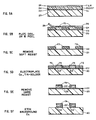
- a pattern plating method is shown in Fig. 5A-5F employing the direct from CAD in situ photo-mask technique of the present invention.
- a substrate 20 carries an upper layer of foil 22, a resist layer 24 and an image developing film layer 26.
- the configuration is identical to that shown in Fig. 1A, except that, when using a negative working resist, the film is preferably a negative-type strip base film rather than a positive-type strip base film as shown in Fig. 1A.
- the film layer is exposed (plotted) and developed on the board as shown in Fig. 5B to produce the image 70.
- the board is then exposed to a UV source to polymerize the unshielded portions of the resist layer 24.
- the film 26, having served its purpose is peeled off and discarded.
- the unpolymerized resist is removed in Fig. 5C leaving areas of hardened resist 72 above the uniform layer of copper 22.
- electroplating can he employed. Through holes (not shown) are plated along with the copper channels exposed through the resist. Those areas covered by resist 72 are not affected by electroplating. This is advantageous since, as only the conductor pattern (and holes) are plated, there is no extraneous electroplated copper to be removed.
- a coating 74 of tin-solder is electroplated in an appropriate bath onto the upper surface of the copper conductors 22'.
- the tin-solder coating 74 clads the desired conductor pattern.
- the structure is placed in an etching bath.
- the tin-solder coating 74 acts as a resist to the copper etchant.
- the copper foil layer 22 is removed everywhere except where the pattern has been plated with tin-solder, thus leaving the desired tin-clad copper pattern as shown in Fig. 5F.
- the structure is heated by IR or hot oil treatment to reflow the tin-solder layer 74 over the etched edges 76 (Fig. 5F) of the copper pattern.
- the photoplotted in situ mask provides the basis for high precision interlayer registration and multilayer printed wiring boards.
- the film exposure is inspectable and stable prior to resist exposure.
- Inspectability is a particularly important advantage over UV plotting.
- An error or artifact in the UV polymerized pattern cannot easily be surgically removed. Instead, the resist must be dissolved away and reapplied after cleaning and drying the board, or the board must simply be discarded.
- the consequences of misplotting UV sensitive PDF layers are serious indeed.
- the onboard developed film can be easily checked for artifacts produced by a plotting glitch, hair, dust, etc.
- the in situ photo-mask can be retouched by using a UV opaque fountain pen or by excising tiny portions of falsely exposed emulsion with an exacto knife.
- the bad mask can be quickly peeled off to try again with a new piece of film. The important difference is that the UV sensitive layer remains undisturbed even though the board is directly plotted from a CAD layout.
- the system can be further adapted to a high speed raster scan system for production use without any of the limitations of current laser equipment.
- a white light source under consideration is a Xenon strobe lamp, beam collimated.
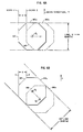
- a raster scan plotter can be equipped with a simple white light source with an octagonal aperture preferably in the form of a stencil.
- the octagonal spot is focused on the emulsion in the film.
- the scan direction is along the y axis as indicated and the objective is to draw or image a line in the x direction.
- the strobe lamp is triggered at precisely the correct y coordinate (y1 in Fig.
- the amount of overlap at the sides is greater for the 90° path (Fig. 6A) than for the 45° path (Fig. 6B).
- This effect can be eliminated by employing diagonal sides, relative to the scan direction, in equal lengths which bear a ratio of approximately the square root of two to the orthogonal sides as shown in Figs. 7A and 7B.
- the octagon will be evenly divided into thirds so that the overlap will be identical when making diagonal and orthogonal lines. However, if the width of the orthogonal line is 3 units, the width of the resulting diagonal line would be 2.828 units.
- the widths could be made equal, however, by changing the magnification if the raster plotter had an automatic zoom lens, for example, or by proper adjustment of the duration of the exposure to allow the light to sweep out a slightly extended octagon in the Y-direction to compensate for its diminished diagonal width when constructing diagonal lines.
- the in situ mask system can accommodate positive or negative type strip base film. Since the majority of available resists used today are negative working, positive strip base film is preferred for subtractive processes. Negative-type strip base film would be used in an identical manner if the boards were fabricated using a pattern plating process as shown in Figs. 5A-5F with negative working resist.
- in situ film mask PWB system is intended to be illustrative and not restrictive.
- double sided boards can be made by applying the same process simultaneously or in sequence to both sides of a substrate.
- Many variations on or addition to the steps or materials described herein are possible within the scope of the present invention.
Landscapes
- Engineering & Computer Science (AREA)
- Physics & Mathematics (AREA)
- General Physics & Mathematics (AREA)
- Architecture (AREA)
- Structural Engineering (AREA)
- Manufacturing & Machinery (AREA)
- Microelectronics & Electronic Packaging (AREA)
- Exposure And Positioning Against Photoresist Photosensitive Materials (AREA)
- Manufacturing Of Printed Circuit Boards (AREA)
- Testing Of Short-Circuits, Discontinuities, Leakage, Or Incorrect Line Connections (AREA)
Priority Applications (1)
| Application Number | Priority Date | Filing Date | Title |
|---|---|---|---|
| AT87900544T ATE101732T1 (de) | 1985-06-10 | 1987-07-05 | Bildaufzeichnungsverfahren fuer gedruckte schaltungen. |
Applications Claiming Priority (2)
| Application Number | Priority Date | Filing Date | Title |
|---|---|---|---|
| US06/742,742 US4666818A (en) | 1985-06-10 | 1985-06-10 | Method of patterning resist for printed wiring board |
| PCT/US1986/002709 WO1988004797A1 (en) | 1985-06-10 | 1986-12-17 | Method of patterning resist for printed wiring board |
Publications (2)
| Publication Number | Publication Date |
|---|---|
| EP0339020A1 EP0339020A1 (en) | 1989-11-02 |
| EP0339020B1 true EP0339020B1 (en) | 1994-02-16 |
Family
ID=24986015
Family Applications (1)
| Application Number | Title | Priority Date | Filing Date |
|---|---|---|---|
| EP87900544A Expired - Lifetime EP0339020B1 (en) | 1985-06-10 | 1987-07-05 | Method of patterning resist for printed wiring board |
Country Status (8)
| Country | Link |
|---|---|
| US (1) | US4666818A (da) |
| EP (1) | EP0339020B1 (da) |
| JP (1) | JPH02501427A (da) |
| KR (1) | KR940007800B1 (da) |
| DE (1) | DE3689659T2 (da) |
| DK (1) | DK170480B1 (da) |
| NO (1) | NO883643L (da) |
| WO (1) | WO1988004797A1 (da) |
Families Citing this family (30)
| Publication number | Priority date | Publication date | Assignee | Title |
|---|---|---|---|---|
| US5254435A (en) * | 1985-06-10 | 1993-10-19 | The Foxboro Company | Method of patterning resist |
| US5015553A (en) * | 1985-06-10 | 1991-05-14 | The Foxboro Company | Method of patterning resist |
| US5302494A (en) * | 1985-06-10 | 1994-04-12 | The Foxboro Company | Multilayer circuit board having microporous layers and process for making same |
| IL81157A (en) * | 1987-01-05 | 1990-04-29 | Uri Shoshani | Decorative products made of plastic having a metallic decorative pattern |
| WO1988005559A1 (en) * | 1987-01-22 | 1988-07-28 | The Foxboro Company | Method of patterning resist |
| CA1249065A (en) * | 1987-07-06 | 1989-01-17 | Allan R. Drake | Process for forming silver conductors on a substrate |
| US4999277A (en) * | 1988-02-22 | 1991-03-12 | Trw Inc. | Production of precision patterns on curved surfaces |
| JPH0234984A (ja) * | 1988-04-13 | 1990-02-05 | Mitsubishi Electric Corp | プリント回路基板の製造方法 |
| US4987050A (en) * | 1988-12-06 | 1991-01-22 | Fuji Photo Film Co., Ltd. | Light-sensitive transfer material and image-forming process using the same |
| US5260168A (en) * | 1989-10-13 | 1993-11-09 | The Foxboro Company | Application specific tape automated bonding |
| EP0448702B1 (en) * | 1989-10-13 | 1995-08-09 | The Foxboro Company | Application specific tape automated bonding |
| DE69024347T2 (de) * | 1989-10-30 | 1996-06-05 | Foxboro Co | Mehrschichtleiterplatte mit mikroporösen schichten und verfahren zur herstellung |
| EP0433721A3 (en) * | 1989-12-22 | 1992-07-08 | Siemens Aktiengesellschaft | Method of applying a solder stop coating on printed circuit boards |
| EP0486246A1 (en) * | 1990-11-14 | 1992-05-20 | Canon Kabushiki Kaisha | Heat-developable photosensitive material |
| US5384230A (en) * | 1992-03-02 | 1995-01-24 | Berg; N. Edward | Process for fabricating printed circuit boards |
| US5751594A (en) * | 1993-03-16 | 1998-05-12 | Emc Corporation | Aperture control system for printed circuit board fabrication |
| JP3149289B2 (ja) * | 1993-03-24 | 2001-03-26 | 三菱製紙株式会社 | 画像形成材料及びそれを使用する画像形成方法 |
| DE4408507A1 (de) * | 1994-03-14 | 1995-09-28 | Heidelberg Instruments Mikrotechnik Gmbh | Lithografisches Verfahren |
| US5712613A (en) * | 1995-05-05 | 1998-01-27 | Mcdonnell Douglas Corporation | Computer-aided method for producing resistive tapers and resistive taper produced thereby |
| EP0785474A1 (de) * | 1996-01-16 | 1997-07-23 | Schablonentechnik Kufstein Aktiengesellschaft | Verfahren und Vorrichtung zur Herstellung einer Flexodruckschablone |
| US6132588A (en) * | 1996-08-09 | 2000-10-17 | Matsushita Electric Works, Ltd. | Method for plating independent conductor circuit |
| WO2001051276A2 (en) * | 2000-01-07 | 2001-07-19 | President And Fellows Of Harvard College | Fabrication of metallic microstructures via exposure of photosensitive composition |
| JP3657168B2 (ja) | 2000-02-28 | 2005-06-08 | 富士通株式会社 | 多層プリント配線板の製造方法 |
| TW200507131A (en) | 2003-07-02 | 2005-02-16 | North Corp | Multi-layer circuit board for electronic device |
| WO2005092043A2 (en) * | 2004-03-22 | 2005-10-06 | Epic Research Company, Inc. | Process for fabrication of printed circuit boards |
| US8142987B2 (en) * | 2004-04-10 | 2012-03-27 | Eastman Kodak Company | Method of producing a relief image for printing |
| KR100697601B1 (ko) | 2004-07-10 | 2007-03-21 | 지성우 | 명함 제조 방법 |
| JP2009239070A (ja) * | 2008-03-27 | 2009-10-15 | Fujifilm Corp | 配線形成方法 |
| CN108650797A (zh) * | 2018-06-22 | 2018-10-12 | 赣州中盛隆电子有限公司 | 一种电路板负片图形转移工艺 |
| CN118315120B (zh) * | 2024-06-07 | 2024-08-30 | 珠海智锐科技有限公司 | 一种柔性透明导电薄膜及其制备工艺 |
Family Cites Families (12)
| Publication number | Priority date | Publication date | Assignee | Title |
|---|---|---|---|---|
| AT326703B (de) * | 1971-10-07 | 1975-12-29 | Zimmer Peter | Verfahren zur herstellung von druckformen |
| US3867150A (en) * | 1973-06-08 | 1975-02-18 | Grace W R & Co | Printing plate process and apparatus using a laser scanned silver negative |
| US4168980A (en) * | 1977-08-19 | 1979-09-25 | Eastman Kodak Company | Heat developable photographic material and process |
| US4419675A (en) * | 1979-05-24 | 1983-12-06 | American Hoechst Corporation | Imaging system and method for printed circuit artwork and the like |
| JPS5660442A (en) * | 1979-10-23 | 1981-05-25 | Fuji Photo Film Co Ltd | Photosensitive lithographic plate and method for making lithographic plate |
| JPS56129394A (en) * | 1980-03-14 | 1981-10-09 | Dainippon Screen Mfg | Method of producing through hole of printed board |
| US4373018A (en) * | 1981-06-05 | 1983-02-08 | Bell Telephone Laboratories, Incorporated | Multiple exposure microlithography patterning method |
| JPS5965838A (ja) * | 1982-10-07 | 1984-04-14 | Dainippon Screen Mfg Co Ltd | 多層構造を有する感材およびその製版方法 |
| JPS5973748U (ja) * | 1982-11-11 | 1984-05-18 | 大日本スクリ−ン製造株式会社 | 色校正用フイルム |
| US4515877A (en) * | 1982-11-27 | 1985-05-07 | Basf Aktiengesellschaft | Image-recording materials and image-recording carried out using these to produce an optical mask |
| JPH0664341B2 (ja) * | 1983-01-24 | 1994-08-22 | ウエスターン エレクトリック カムパニー,インコーポレーテッド | 半導体デバイスの製作法 |
| US4469777A (en) * | 1983-12-01 | 1984-09-04 | E. I. Du Pont De Nemours And Company | Single exposure process for preparing printed circuits |
-
1985
- 1985-06-10 US US06/742,742 patent/US4666818A/en not_active Expired - Lifetime
-
1986
- 1986-12-17 WO PCT/US1986/002709 patent/WO1988004797A1/en not_active Ceased
- 1986-12-17 DE DE3689659T patent/DE3689659T2/de not_active Expired - Fee Related
- 1986-12-17 KR KR1019880700996A patent/KR940007800B1/ko not_active Expired - Fee Related
- 1986-12-17 JP JP62500562A patent/JPH02501427A/ja active Pending
-
1987
- 1987-07-05 EP EP87900544A patent/EP0339020B1/en not_active Expired - Lifetime
-
1988
- 1988-08-16 DK DK457988A patent/DK170480B1/da active
- 1988-08-16 NO NO88883643A patent/NO883643L/no unknown
Non-Patent Citations (1)
| Title |
|---|
| Patent Abstracts of Japan, volume 4, no. 86, 20 June 1980, page 136P16 & JP, A, 55 502 46 * |
Also Published As
| Publication number | Publication date |
|---|---|
| WO1988004797A1 (en) | 1988-06-30 |
| EP0339020A1 (en) | 1989-11-02 |
| DK170480B1 (da) | 1995-09-11 |
| JPH02501427A (ja) | 1990-05-17 |
| DE3689659D1 (de) | 1994-03-24 |
| DK457988D0 (da) | 1988-08-16 |
| KR890700855A (ko) | 1989-04-27 |
| DE3689659T2 (de) | 1994-09-29 |
| US4666818A (en) | 1987-05-19 |
| NO883643L (no) | 1988-10-14 |
| KR940007800B1 (ko) | 1994-08-25 |
| DK457988A (da) | 1988-08-16 |
| NO883643D0 (no) | 1988-08-16 |
Similar Documents
| Publication | Publication Date | Title |
|---|---|---|
| US4666818A (en) | Method of patterning resist for printed wiring board | |
| US5015553A (en) | Method of patterning resist | |
| US5384230A (en) | Process for fabricating printed circuit boards | |
| US4961259A (en) | Method of forming an interconnection by an excimer laser | |
| US5464662A (en) | Fabrication method of printed wiring board | |
| JPH06216479A (ja) | プリント回路基板とその製造方法 | |
| US5254435A (en) | Method of patterning resist | |
| KR950003244B1 (ko) | 다층 회로판 제조공정 | |
| JP3031042B2 (ja) | 表面実装用プリント配線板 | |
| AU612563B2 (en) | Method of patterning resist for printed wiring board | |
| JPH0537140A (ja) | プリント配線板の製造方法 | |
| EP0346355B1 (en) | Photopatternable composite | |
| WO1988005252A1 (en) | Method for the manufacture of multilayer printed circuit boards | |
| CA1283574C (en) | Method of patterning resist for printed wiring boards | |
| CN87100339A (zh) | 印刷线路板的图案抗蚀法 | |
| JPH11274698A (ja) | プリント配線板の製造方法 | |
| JP3657168B2 (ja) | 多層プリント配線板の製造方法 | |
| JPH04326588A (ja) | 印刷配線板の製造方法 | |
| JPH05267848A (ja) | 印刷配線板の製造方法 | |
| JPH05243716A (ja) | 配線板の製造方法 | |
| JPH09142052A (ja) | スクリーン版およびその製造方法とそれを用いたプリント配線板の製造方法 | |
| JPH05206644A (ja) | 印刷配線板の製造方法 | |
| JPS63150993A (ja) | プリント配線板の製造方法 | |
| JPH0567871A (ja) | 印刷配線板及びその製造方法 | |
| JPS59214294A (ja) | プリント回路板の製造方法 |
Legal Events
| Date | Code | Title | Description |
|---|---|---|---|
| PUAI | Public reference made under article 153(3) epc to a published international application that has entered the european phase |
Free format text: ORIGINAL CODE: 0009012 |
|
| 17P | Request for examination filed |
Effective date: 19890703 |
|
| AK | Designated contracting states |
Kind code of ref document: A1 Designated state(s): AT BE CH DE FR GB IT LI LU NL SE |
|
| 17Q | First examination report despatched |
Effective date: 19920110 |
|
| GRAA | (expected) grant |
Free format text: ORIGINAL CODE: 0009210 |
|
| AK | Designated contracting states |
Kind code of ref document: B1 Designated state(s): AT BE CH DE FR GB IT LI LU NL SE |
|
| PG25 | Lapsed in a contracting state [announced via postgrant information from national office to epo] |
Ref country code: NL Effective date: 19940216 Ref country code: CH Effective date: 19940216 Ref country code: AT Effective date: 19940216 Ref country code: IT Free format text: LAPSE BECAUSE OF FAILURE TO SUBMIT A TRANSLATION OF THE DESCRIPTION OR TO PAY THE FEE WITHIN THE PRE;WARNING: LAPSES OF ITALIAN PATENTS WITH EFFECTIVE DATE BEFORE 2007 MAY HAVE OCCURRED AT ANY TIME BEFORE 2007. THE CORRECT EFFECTIVE DATE MAY BE DIFFERENT FROM THE ONE RECORDED.SCRIBED TIME-LIMIT Effective date: 19940216 Ref country code: LI Effective date: 19940216 Ref country code: SE Effective date: 19940216 Ref country code: BE Effective date: 19940216 |
|
| REF | Corresponds to: |
Ref document number: 101732 Country of ref document: AT Date of ref document: 19940315 Kind code of ref document: T |
|
| ET | Fr: translation filed | ||
| REF | Corresponds to: |
Ref document number: 3689659 Country of ref document: DE Date of ref document: 19940324 |
|
| REG | Reference to a national code |
Ref country code: CH Ref legal event code: PL |
|
| NLV1 | Nl: lapsed or annulled due to failure to fulfill the requirements of art. 29p and 29m of the patents act | ||
| PLBE | No opposition filed within time limit |
Free format text: ORIGINAL CODE: 0009261 |
|
| STAA | Information on the status of an ep patent application or granted ep patent |
Free format text: STATUS: NO OPPOSITION FILED WITHIN TIME LIMIT |
|
| PG25 | Lapsed in a contracting state [announced via postgrant information from national office to epo] |
Ref country code: LU Free format text: LAPSE BECAUSE OF NON-PAYMENT OF DUE FEES Effective date: 19941231 |
|
| 26N | No opposition filed | ||
| PGFP | Annual fee paid to national office [announced via postgrant information from national office to epo] |
Ref country code: GB Payment date: 19981110 Year of fee payment: 13 |
|
| PGFP | Annual fee paid to national office [announced via postgrant information from national office to epo] |
Ref country code: FR Payment date: 19981203 Year of fee payment: 13 |
|
| PGFP | Annual fee paid to national office [announced via postgrant information from national office to epo] |
Ref country code: DE Payment date: 19981230 Year of fee payment: 13 |
|
| PG25 | Lapsed in a contracting state [announced via postgrant information from national office to epo] |
Ref country code: GB Free format text: LAPSE BECAUSE OF NON-PAYMENT OF DUE FEES Effective date: 19991217 |
|
| GBPC | Gb: european patent ceased through non-payment of renewal fee |
Effective date: 19991217 |
|
| PG25 | Lapsed in a contracting state [announced via postgrant information from national office to epo] |
Ref country code: FR Free format text: LAPSE BECAUSE OF NON-PAYMENT OF DUE FEES Effective date: 20000831 |
|
| PG25 | Lapsed in a contracting state [announced via postgrant information from national office to epo] |
Ref country code: DE Free format text: LAPSE BECAUSE OF NON-PAYMENT OF DUE FEES Effective date: 20001003 |
|
| REG | Reference to a national code |
Ref country code: FR Ref legal event code: ST |