EP0350919A2 - Appareil de production d'images à couleurs - Google Patents
Appareil de production d'images à couleurs Download PDFInfo
- Publication number
- EP0350919A2 EP0350919A2 EP89112852A EP89112852A EP0350919A2 EP 0350919 A2 EP0350919 A2 EP 0350919A2 EP 89112852 A EP89112852 A EP 89112852A EP 89112852 A EP89112852 A EP 89112852A EP 0350919 A2 EP0350919 A2 EP 0350919A2
- Authority
- EP
- European Patent Office
- Prior art keywords
- color
- region
- pixel
- marker
- information
- Prior art date
- Legal status (The legal status is an assumption and is not a legal conclusion. Google has not performed a legal analysis and makes no representation as to the accuracy of the status listed.)
- Granted
Links
Images


Classifications
-
- H—ELECTRICITY
- H04—ELECTRIC COMMUNICATION TECHNIQUE
- H04N—PICTORIAL COMMUNICATION, e.g. TELEVISION
- H04N1/00—Scanning, transmission or reproduction of documents or the like, e.g. facsimile transmission; Details thereof
- H04N1/387—Composing, repositioning or otherwise geometrically modifying originals
- H04N1/3872—Repositioning or masking
-
- G—PHYSICS
- G03—PHOTOGRAPHY; CINEMATOGRAPHY; ANALOGOUS TECHNIQUES USING WAVES OTHER THAN OPTICAL WAVES; ELECTROGRAPHY; HOLOGRAPHY
- G03G—ELECTROGRAPHY; ELECTROPHOTOGRAPHY; MAGNETOGRAPHY
- G03G15/00—Apparatus for electrographic processes using a charge pattern
- G03G15/01—Apparatus for electrographic processes using a charge pattern for producing multicoloured copies
-
- H—ELECTRICITY
- H04—ELECTRIC COMMUNICATION TECHNIQUE
- H04N—PICTORIAL COMMUNICATION, e.g. TELEVISION
- H04N1/00—Scanning, transmission or reproduction of documents or the like, e.g. facsimile transmission; Details thereof
- H04N1/46—Colour picture communication systems
- H04N1/56—Processing of colour picture signals
- H04N1/58—Edge or detail enhancement; Noise or error suppression, e.g. colour misregistration correction
Definitions
- the present invention relates to a color image processing apparatus which is peculiarly well fitted for an image processing apparatus such as a color copier in which a plain paper is used as a recording paper.
- the invention especially relates to a color image processing apparatus in which the region designating information can be accurately detected.
- color image information is obtained by dissolving plural colors on a color document, and color images are recorded according to the color image information.
- a color copier of this kind is designed and made so that it can conduct various image processing such as variable magnification processing and partial color conversion processing.
- Partial color conversion processing means an image compiling process in which the color image information inside or outside the designated region can be recorded by the color by which the region is designated.
- Designation of the region is usually conducted by a color marker.
- a color marker For instance, in the case the region a is designated by a blue marker as shown in Fig. 20A, the image within the region a is recorded by the color which was used to designate the region, which is blue in this example. Refer to Fig. 20B.
- the images in the region can be recorded as black and white images.
- Fig. 21 In order to attain the partial color conversion mode, it is necessary to detect the color of a color marker used to designate the region and region itself respectively. In order to obtain the object, an example is shown in Fig. 21. As shown in Fig. 21, the marker signals BP, RP are detected from the color marker which each scanning line (n, n+1, and so forth) and at the same time the region signals QB′, QR′ are generated by the process.
- the apparatus can not convert colors within the designated region correctly unless the image information of a document and that of a color marker are discriminated accurately.
- the information obtained is not color marker information, but document image information.
- the color mark's information is obtained in the edges of both sides of the crossing area contour, but the color mark information can not be obtained within the crossing area.
- the color marker information is broken off at this crossing area and the color conversion processing is not properly conducted there.
- a color image processing apparatus equipped with a partial color conversion processing function, which can detect the color marker accurately.
- a color image processing apparatus in which color image information converted to an electric signal is processed, comprising; a color discriminating means; a color ghost correction means; an image processing means by which an image processing of a designated region is conducted according to color information different from the color of a document to be read out; and at least a part of the color information of the document which comes into contact with the region designating color information, is changed to the color information to designate the region.
- Another characteristic of the image processing apparatus of the present invention is explained as follows. In the image processing apparatus mentioned above, the document color information sandwiched between the color information which designates the region, can be changed to the information to designate the region.
- the marker correction circuit 600 is installed in order to accurately detect the color marker region. Refer to Fig. 12.
- the image data of a single pixel which corresponds to several pixels or several lines is referred. If the color information comes into contact with the color marker information to designate the region, this color information is changed to the color marker information. In other words, replacement of data. Furthermore, when there exists document color information sandwiched between the color marker information, the sandwiched color information is changed to the information of a color marker.
- the color information correcting table is provided in the marker correction circuit 6oO.
- the target pixel is changed to the color information of the color marker. Refer to Fig. 10.
- the target pixel After the target pixel is changed to the color information of the color marker, even in the case the image information of the document crosses the color marker, the color marker data does not break. Therefore, the designated region can be accurately detected.
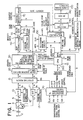
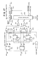
- FIG. 1 an example of the color image processing apparatus relarted to the present invention which is applied to a color copy machine is explained.
- Fig. 1 The configuration of the color image processing apparatus is presented in Fig. 1.
- the color image information in other words optical image information, on the document and an another subject 2 is separated into two color separation images by the dichroic mirror 4 through the optical system 3.
- color image information is separated into red R and cyan Cy color separation images. This color separation is conducted by use of the dichroic mirror 4 having a cut off range of 540 to 600mm.
- Red R and cyan Cy color separation images are supplied to such image reading units as CCDs 6 and 7 through which image signals of red component R and cyan component Cy are provided.
- Image signals R and Cy are supplied to analog/digital converters 10 and 11 where they are converted into digital signals with predetermined bits, 6 bits in this example. At the time, shading correction is conducted.
- the numerals 12 and 13 show shading correction circuits.
- VR and VC are supplied into the color separating circuit or color discriminating circuit 20 where they are discriminted as one of multiple color signals.
- This example shows a configuration to discriminate an image signal as one of the color signals: red, blue and black. Namely, possible colors of original images on a document are respectively discriminated per pixel as one of predetermined colors such as red, blue or black. Through this discriminating operation, the document is deemed to consist of images whose color is one of red, blue or black colors.
- the above predetermined colors are determined as red, blue and black color on the basis of recording colors of a recording apparatus, however, it is possible to use more than four colors including those three colors.
- Each discriminated color signal consists of color code data. which is 2-bit data, and density data, which is 6-bit data.
- color code data which is 2-bit data
- density data which is 6-bit data.
- data of each color signal that stored in the color discrimination converting table or map constituted with ROM, is used for example.
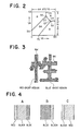
- Fig. 2 is one of the examples of the color discrimination maps.
- the system can be organized so that a plurality of color discrimination converting tables are prepared and one out of these is chosen according to the record mode for example.
- the table is chosen by a signal from a microcomputer which will be explained later.
- Color discriminated image data is transferred to the color image processing step.
- the image data is supplied to the color ghost correction means 300 of the next stage where color ghost correction is conducted in the primary scanning direction, in other words, in the horizontal scanning direction, and in the secondary scanning direction, in other words, in the drum revolution direction.
- This color ghost correction is made to prevent undesirable color ghost around letters, especially black letters, during color separation, in other words, color discrimination.
- Fig. 3 explains how color ghosts appear after a black Japanese letter " " (sei, gender) was photographed and its color was discriminated.
- the color ghost correction means 300 is the circuit to correct the above-mentioned color ghost as much as possible.
- the color ghost correction processing aims at only the color code data.
- the color pattern method is used since fixed color ghost appears for the original color, for example: Original: Black - Color ghost: Red and blue Original: Red, blue - Color ghost: Black with the color pattern method, the original color can be identified by knowing how a color for a certain pixel and those for its surrounding pixels appears (pattern).
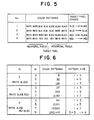
- Fig. 5 shows an example which determines the color pattern of the target pixel and its surrounding pixels, and the color of the target pixel to be determined at that time.
- this example uses LUT look-up table) in ROM form.
- One or two-dimensional systems can be used for color pattern. Assuming that the number of colors is N and the number of surrounding pixels including that pixel is M, the number of color pattern is: N M
- Fig. 6 indicates the relationship between size and color pattern.
- This example uses a color pattern with a size of 1 x 7, as described above; however, use of color patterns with smaller sizes, like one with 1 x 5, is possible.
- the color pattern with a size of 1 x 5 can eliminate color ghost of a single pixel, while the color pattern with a size of 1 x 7 can eliminate color ghost of two pixels.
- the color code is entered as an ROM address.
- the color pattern is thus: White White Blue Blue Black Black Black 11 11 01 01 00 00 00
- the address is: D40
- the address contains the black code: 00
- a bipolar ROM Since a 14-bit address is required for a pattern of 1 x 7 , a bipolar ROM should meet the demand for entry of an address of 14 bits and a color code of 2 bits. However, bipolar ROMS with such a large capacity cannot br easily found and would be very expensive. The output of ROM is generally 8-bit.
- the working example shows the case where ROM is searched by the first one pixel, and six other pixel codes are used to perform table look-up work.
- the output data of ROM, D0, D1 is searched when the lead pixel is black.
- the output data, D2, D3 is searched when the lead pixel is blue.
- the output data, D4, D5 is searched when the lead pixel is red.
- the output data, D6, D7 is searched when the lead pixel is white.
- the lead pixel is white in the color pattern in Fig. 5, both of bit D6 and bit D7 out of the output of ROM are searched. But even if the lead pixel is white and the output bit D6, D7 is searched, the target pixel color codes are different from each other as shown in Fig. 5.
- the ROM addresses to be referred to are different from each other according to the combination of pixels to be input.
- the combination of pixels means the combination of color data codes.
- the image data after color ghost correction was made which consists of the color code data and the density data, is processed in the resolution correction circuit 40.
- the density data is processed and the resolution, which is called MTF, is corrected.
- the factors to deteriorate resolution are problems in the optical system, the optical running system, the signal processing system, and the recording system.
- the optical system and the optical running system among others directly influence deterioration of resolution.
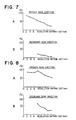
- Fig. 7 represents MFT values of the primary scanning direction and the secondary scanning direction before resolution correction was made.
- the data shown in the charts is the result of measurements made when a black and white image pattern with spatial frequency from 2dots/mm to 16dots/mm was scanned.
- Deterioration in MTF is more obvious in the secondary scan direction than in the primary scan direction.
- the amount of correction in the secondary scanning direction is preferably adjusted to be twice to four times as much as that in the primary direction.
- the resolution correction means is constituted by adopting a convolution filter with 3x3 pixel.
- the density data and color code data after the resolution was corrected are supplied to the color data selector 50, and when partial color conversion mode is selected, the image region is recorded with a specific color.
- the region extract circuit 60 is installed in the apparatus and the color marker region on the document is detected.
- the region signals QR′ and QB′ which are obtained by this detection are supplied to the data selector 50. Please refer to Fig. 21 as far as this matter is concerned.
- the scan code signal which indicates the color in which images are being copied at the present time and the partial color conversion signal CC are respectively supplied to the data selector 50.
- the scan code signal indicates the color in which the image is being developed at the present time in the case of a multicolor copy machine which can record a plurality of specific colors, develops a color at every revolution of the photoreceptor, and transfers the images on the photoreceptor to a recording paper after all colors have been developed.
- a blue marker when detected, it indicates that the machine is set to blue color copy sequence. If the necessary color data is output when the region signal is obtained, the images within the blue color marker are recorded in blue color.
- the copy machine is not set to partial color conversion mode, only color code data which accords with the scan code is sent and the density data is output.
- the necessary density data is selectively output only when the red color code is obtained.
- the image data in other words the density data, which was output from the color data selector 50, is magnified or reduced by the variable magnification circuit 70.
- Magnifying and reducing processes are conducted as follows.
- the density data is interpolated in the primary scan direction and the scan speed is controlled in the secondary scan direction, in other words the photoreceptor rotating direction.
- the sampling data in the secondary scan direction is thinned out. So, the images are reduced. On the contrary, if the scan speed is decreased, the images are magnified.
- the color code data is simultaneously magnified or reduced, then it is supplied to the multivalued circuit 80.
- the threshold data is set manually or automatically.
- the histogram making circuit 100 is installed.
- the density histogram shown in Fig. 9 is made from the histogram making circuit 100 or the image data obtained.
- the most adequate threshold data to the image is computed according to the density histogram.
- the multivalued 3-bit density data is supplied to the driver 140 through the interface circuit 130.
- Laser beams are modulated in accordance with the multivalued data at the driver 140.
- it is PWM-modulated.
- the driver 140 can be built in the multivalue circuit 80.
- Latent images are formed by PWM-modulated laser beams on a photoreceptor drum which is installed in the output unit 150.
- the image transfer drum which has been used in the conventional color image forming method, is not used in this case.
- three color images consisting of blue, red and black, are developed on an image forming OPC photoreceptor drum while the drum rotates three times. After development, the images are transferred on a plain recording paper.
- the numeral 170 is a timing signal generating circuit by which various timing can be obtained.
- the horizontal and vertical synchronizing signals, HV, VV related to the primary and secondary scan directions which are sent from the output unit 150 including the clock CLK and the index signal, IDX which indicates the start of scanning by laser beams, are supplied to the timing signal generating circuit. According to these signals, the timing signal to start reading CCD 6, 7 is determined.
- the numeral 180 is a timing signal generating circuit to produce a variable magnification signal.
- the apparatus when the partial color conversion mode is selected and a region on the document is designated by a color marker, wherein the color marker crosses a ruled line as shown in Fig. 22, the apparatus automatically detects the crossing area and changes the image data to the color information of the color marker.
- color marker information which corresponds to at least a pixel exists.
- the color information correspoding to the portion of at least several pixels which is different from the color information mentioned above, is continuously detected out of the color marker information.
- a red color marker is used in Fig. 10-a
- a blue color marker can be used in the same way as a red color marker.
- the marker signals BP, RP actually the color code data, wherein the signal represents the color marker region as shown in Fig. 21, and the region signals QB′, QR′ which represent the region a must be detected respectively.
- the color data selector 50 is installed in the apparatus in addition to the region extracting circuit 60 as shown in Fig. 1.
- the color data selector 50 is the circuit for selecting the developing color density data corresponding to the copy sequence, in other words it is the developing sequence, when the partial color is designated, and it is the circuit for selecting the developing color density data corresponding to the copy sequence, when the normal copy is conducted.
- FIG. 11 A concrete example of the region extracting circuit 60 is shown in Fig. 11.
- the bit data of the color code obtained by scanning the color marker is supplied to the color marker correcting circuit 600 and the color information replacement processing mentioned above is conducted.
- the color code data is supplied to the color marker detecting circuit 501 and the data is investigated as to whether a specific color marker is contained in it or not.
- this process is applied to two color markers, a red one and a blue one. As a result, two color marker signals, BP and RP, are detected.
- the marker signals RP, BP are supplied to the region extracting unit 520 and the region signals QR′, QB′ indicating the designated region a are output at each scanning line.
- Fig. 12 is one of the examples of the color marker correcting circuit 600.
- the range of the pixels to be corrected depends on the kind of document to be used.
- the thickness of ruled lines of an ordinary paper for office use is 0.2mm through 0.3mm and the thickness of a line drawn by a plotter available on the market is 0.2mm through 0.5mm. For that reason, the limit of the correcting range is set to 0.5mm in the example.
- the image data corresponding to 8 pixels is converted in parallel with regard to the primary scanning direction and the secondary scanning direction respectively.
- the input color code is supplied to the first stage input terminals of the latch circuit 602. Then, the color code which is output from this, is supplied to the second stage input terminals. The same processing is conducted continuously until the last stage, the eighth stage.
- each output terminal can be provided with the output color code which is obtained by shifting the input color code pixel by pixel in order.
- the color codes corresponding to 8 pixels are arranged in parallel and the data is supplied to the correcting table 603.
- the correcting data is referred in this way.
- the color codes to be used for correction are held in the form of tables in the apparatus, so that the black color code can be changed to the color code of a color marker when the black color code, which is image information, is input as shown in Fig. 10.
- the line memory 605 to arrange data in parallel and the correcting table 606 are installed in the apparatus.
- the correcting table is referred according to the color code data corresponding to 8 lines which are arranged in parallel and the color code data of the checked pixels is changed to the color code data of the color marker.
- the color data converting table shown in Fig. 10 is used in this case.
- the structure of the line memory 605 is 8-line line memories arranged in tandem.
- the latch circuit 602 can be made of 7 latch circuits arranged in tandem.
- the color marker detecting process is conducted.
- Fig. 13 is one of the examples of the color marker detecting circuit 501.
- the color code data of blue is 01 and the color code data of red is 10.
- phase inverter 511 the phase of the high-order bit color code data and that of the low-order bit color code data are inverted by the phase inverter 511.
- the inverted data is supplied to the NAND circuit 513.
- phase of the low-order bit data and that of the high-order bit data are inverted by the phase inverter 512.
- the inverted data is supplied to the other NAND circuit 514.
- the output of the vertical valid area signal V-VALID and AND output of the size signal B4 are supplied to the NAND circuits 513 and 514 as the gate signal.
- the numeral 515 represents the AND circuit.
- the blue marker signal BP which has a pulse width corresponding to the thickness of the contour of the color marker, is output from the terminal 516, Refer to Fig. 21.
- the red marker signal RP is output from the other terminal 517. Refer to Fig. 21.
- FIG. 15 One of the examples of the region extracting unit 520 is shown in Fig. 15.
- the region extracting unit 520 consists of the first and the second region extracting unit 520A, 520B. Each region extracting unit has respectively the data storing circuits 521A, 520B and the region computing circuits 521B, 522B.
- the first and the second region extracting units 520A, 520B have the function to extract a red marker region in addition to the function to extract a blue marker region.
- the region signal of the present scanning line is formed by computation using the region signal obtained scanning immediately before the processing and the marker signal obtained by scanning the present scanning line.
- the computing process In order to attain the object, the computing process must be conducted in at least three-line periods. Therefore, the first data storing circuit 521A must comprise; the function to store the region signal over a line which is the last data of the scanning line just before the computing process; the function to store the first and the second region signals, actually NAND output, wherein the first and the second signals are formed by the region signal and the marker signal BP which is obtained by scanning the present scanning line; and the function to store the region signal of the present scanning line which is obtained by computing the region signals explained before.
- the second region signal is formed by reading out the memory in the opposite way, the number of memory to realize the memory function is 16 in total. Furthermore, red markers are needed to be detected. As a result, 32 line memories are needed.
- the first data storing circuit 521A comprises a pair of memories 525, 526 which are respectively constituted by 8 line memories, in other words 8-bit line memories. Since these line memories are selectively used at each line, a pair of three-state buffers 523, 524, a pair of data selectors 527, 528, and the latch circuit 529 are provided with the apparatus.
- the three signals obtained in the first region computing circuit 530B for blue color, are supplied as input signals to the first data storing circuit 521A in addition to the blue marker signal BP.
- the blue marker region signal QB′ on the present scanning line n is formed by the region signal QB which is obtained immediately before the computation and the marker signal BP on the present scanning line.
- a pair of signals QB, BP are supplied to NAND circuit 531, the preset pulse PB1 whch is shown in Fig. 16, is supplied to the preset terminal PR of the D-type flip-flop 532, and the region signal QB just before the computation is supplied to the clear terminal CL.
- the first NAND output BN0 which is the first contour signal, is obtained.
- the first NAND output BN0 and the marker signal BP are stored in the memory 526 in order. Therefore, on the scanning line (n + 1), the three-state buffer 524 is activated. The same processing is also conducted in the second region extracting unit 520B at the same timing. But the installed memories are all address-controlled so that they are written in in the normal direction and read out in the reverse direction. Accordingly, the output timing of the marker signal BP and the region signal QB obtained just before the computation, is W1 on n line. But it is W2 on (n + 1) line. So, it is read out a little earlier. Refer to Fig. 16 H, I. As a result, the output BN1 of the second NAND becomes K shown in Fig. 16. The marker signal BP and the second NAND output BN1 are stored again in the data storing circuit 521B.
- the memory installed in the second region extracting unit 520B is written in the normal direction and read out in the reverse direction. Therefore, the reading out timing W3 of the first NAND output BN1 and the reading out timing W4 of the second NAND output BN2 coincide with each other.
- This OR output QB′ is the signal which indicates the area within the contour of the blue marker drawn on the present scanning line n. In other words, this OR output is the region signal QB′ of the present scanning line.
- region signal QB′ is fed back to the data storing circuit 521A, 521B in order to use the signal as the region signal QB on the next scanning line.
- the marker region is accurately detected by using a pair of NAND outputs BN0, BN1 which are obtained by reversing the direction of reading out the memory.
- the region computing circuit 530R is a NAND circuit
- the numeral 536 is a D-type flip-flop
- the numeral 537 is an AND circuit
- the numeral 538 is an OR circuit.
- QR′ represents the red marker region signal.
- the region signals QB′ and QR′ supplied to the output terminals are supplied to the region determining circuit 540 as shown in Fig. 40.
- the region determining circuit 540 is a control means for the region signal used to record images as shown in Fig. 19, if the marker designation is similar to one shown in Fig. 19A.
- a black image is recorded as a red image.
- a black image is recorded as a blue image by allowing density data gate signal S to be formed from region signals QB′ and QR′.
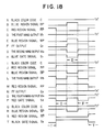
- the region determining circuit 540 has four flip-flops 541 through 544. Region signals QB′ and QR′ latched by the forward flip-flops 541, 542 are supplied to their corresponding NAND circuits 545 through 548. To each of the NAND circuits 45 through 548, color code data C indicating black color is supplied via the AND circuit 554. On the other hand, to the switching circuit 553, the scan code signal is supplied which shows that the copying operation is finished, and in which color.
- the first AND circuit 545 provides the first NAND output M1 as shown in Fig. 18D.
- the second NAND circuit 546 provides the second NAND output M2 shown in Fig. 43G based on the E, F input signals in Figs. 43E, 43F.
- the AND circuit 551 provides the gate signal S1 related to the period III shown by H in Fig. 18.
- J to K input signals in Fig. 18, provide the third NAND output M3 of Fig. 18L, while input signals in Fig. 18M and N provide the fourth NAND output M4 in Fig. 18-O.
- the second AND circuit 552 provides the gate signal S2 (Fig. 18P) related to the periods II and IV.
- the fifth NAND circuit 549 provides the gate signal S3 (Fig. 18T) corresponding to the periods I and V.
- One of the gate signals S1 to S3 is selected by the switching circuit 553 corresponding to the scan code signal that indicates the copy sequence. Accordingly, the gate signal S1 is selected for blue color recording mode. while the gate signal S2 is selected for red color recording mode. Likewise, gate signal S3 is selected for black color recording mode.
- Gate signals S1 to S3 which are output from the switching circuit 553, are supplied to the density data selection circuit 574 shown in Fig. 17, and the density data corresponding to the color code, is selected.
- white density data of white color which is always 1, is selected in the period outside the period where there is no gate signal S.
- white data is always selected outside the period III in the blue color recording mode.
- blue image is recorded in period III alone in the blue recording mode, while red image is recorded in period II and IV in the red recording mode and periods I and V are recorded in black color in the black recording mode (Fig. 19B).
- the density data is delayed by the delay control circuit 575, and the delayed time amounts to 8 lines.
- the delayed density data is input to the selecting circuit 574.
- the reason for delaying the density data is that the color marker data is changed in the direction of the secondary scanning, so it is necessary to adjust the density data timing in accordance with the color marker data.
- the region judging unit 540 even in a double-designated region, the color of an inside color marker has priority over other colors.
- Partial color conversion comprises detecting the designated region and processing of image data or color within the designated region. Therefore, the partial color conversion mode can be used for extracting the partial region, erasing, deleting, reversing, mirror image, magnifying, reducing, position transferring, and optional combinations of them. It is possible to determine the content of processing beforehand and conduct the predetermined processing in the detected region.
- Red and redlike colors such as orange and pink, or blue and bluelike colors are obtained as those colors are hard to copy in the usual copy mode.
- the color information of a document which comes into contact with the color information to designate the region is changed to the region designating color information.
- the color marker information which is hidden by the document color information is positively compensated. Accordingly, it has a characteristic that the designated region of a color marker is accurately detected. Therefore, correct color conversion is conducted.
- the document color information sandwiched between the color information which designates the region can be changed to the color information to designate the region.
- the color information in which one side of the image cotour comes into contact with the color marker is not changed. Therefore, for instance, in case where a color marker is set coming into contact with a horizontal line, the color marker is not changed in the range of the horizontal line region.
- the invention is well fitted for a color image processing apparatus such as a color copier.
Landscapes
- Engineering & Computer Science (AREA)
- Multimedia (AREA)
- Signal Processing (AREA)
- Physics & Mathematics (AREA)
- General Physics & Mathematics (AREA)
- Editing Of Facsimile Originals (AREA)
- Facsimile Image Signal Circuits (AREA)
- Color Image Communication Systems (AREA)
Applications Claiming Priority (4)
| Application Number | Priority Date | Filing Date | Title |
|---|---|---|---|
| JP176750/88 | 1988-07-15 | ||
| JP63176750A JP2557480B2 (ja) | 1988-07-15 | 1988-07-15 | カラー画像処理装置 |
| JP63176751A JP2557481B2 (ja) | 1988-07-15 | 1988-07-15 | カラー画像処理装置 |
| JP176751/88 | 1988-07-15 |
Publications (3)
| Publication Number | Publication Date |
|---|---|
| EP0350919A2 true EP0350919A2 (fr) | 1990-01-17 |
| EP0350919A3 EP0350919A3 (en) | 1990-09-26 |
| EP0350919B1 EP0350919B1 (fr) | 1994-06-08 |
Family
ID=26497539
Family Applications (1)
| Application Number | Title | Priority Date | Filing Date |
|---|---|---|---|
| EP89112852A Expired - Lifetime EP0350919B1 (fr) | 1988-07-15 | 1989-07-13 | Appareil de production d'images à couleurs |
Country Status (3)
| Country | Link |
|---|---|
| US (1) | US5130791A (fr) |
| EP (1) | EP0350919B1 (fr) |
| DE (1) | DE68915871T2 (fr) |
Cited By (1)
| Publication number | Priority date | Publication date | Assignee | Title |
|---|---|---|---|---|
| EP0441575A3 (en) * | 1990-02-05 | 1992-06-03 | Konica Corporation | Color image processing apparatus |
Families Citing this family (9)
| Publication number | Priority date | Publication date | Assignee | Title |
|---|---|---|---|---|
| US5495341A (en) * | 1991-03-06 | 1996-02-27 | Canon Kabushiki Kaisha | Image processing apparatus which selects from one of plural generated clock counts |
| JP2639517B2 (ja) * | 1991-03-12 | 1997-08-13 | 大日本スクリーン製造株式会社 | 画像領域の色付け処理方法 |
| JP2600515B2 (ja) * | 1991-05-14 | 1997-04-16 | 富士ゼロックス株式会社 | 画像処理方法 |
| US5374996A (en) * | 1991-06-26 | 1994-12-20 | Matsushita Electric Industrial Co., Ltd. | Image processing system |
| JP3295970B2 (ja) * | 1992-07-21 | 2002-06-24 | 富士ゼロックス株式会社 | 領域認識装置 |
| EP0643528B1 (fr) * | 1993-09-14 | 2000-06-14 | Canon Kabushiki Kaisha | Appareil de traitement d'image capable de réaliser un marquage d'édition |
| JP3748172B2 (ja) * | 1998-12-09 | 2006-02-22 | 富士通株式会社 | 画像処理装置 |
| JP5147641B2 (ja) * | 2008-10-24 | 2013-02-20 | キヤノン株式会社 | 原稿読取装置 |
| JP2010139619A (ja) * | 2008-12-10 | 2010-06-24 | Konica Minolta Business Technologies Inc | 画像形成装置 |
Family Cites Families (11)
| Publication number | Priority date | Publication date | Assignee | Title |
|---|---|---|---|---|
| US4538182A (en) * | 1981-05-11 | 1985-08-27 | Canon Kabushiki Kaisha | Image processing apparatus |
| JPS59147572A (ja) * | 1983-02-10 | 1984-08-23 | Fuji Xerox Co Ltd | カラ−画情報処理装置 |
| US4720750A (en) * | 1986-02-28 | 1988-01-19 | Kabushiki Kaisha Toshiba | Image forming apparatus |
| JPS62216478A (ja) * | 1986-03-17 | 1987-09-24 | Dainippon Screen Mfg Co Ltd | 網ふせ装置 |
| DE3751614T2 (de) * | 1986-06-30 | 1996-03-28 | Konishiroku Photo Ind | Bildverarbeitungsverfahren und Vorrichtung dazu. |
| EP0268499B1 (fr) * | 1986-11-20 | 1993-10-20 | Konica Corporation | Appareil pour la formation d'images en couleurs |
| DE3787351T2 (de) * | 1986-12-03 | 1994-01-13 | Konishiroku Photo Ind | Farbbildverarbeitungsgerät. |
| WO1988005622A1 (fr) * | 1987-01-27 | 1988-07-28 | Konica Corporation | Processeur d'images en couleurs |
| JPH07101915B2 (ja) * | 1987-09-21 | 1995-11-01 | コニカ株式会社 | 画像処理装置 |
| US4929979A (en) * | 1988-01-29 | 1990-05-29 | Konica Corporation | Method and apparatus for processing image |
| JPH0243873A (ja) * | 1988-08-04 | 1990-02-14 | Ricoh Co Ltd | デジタル複写機におけるマーカ編集方法 |
-
1989
- 1989-07-12 US US07/378,805 patent/US5130791A/en not_active Expired - Lifetime
- 1989-07-13 DE DE68915871T patent/DE68915871T2/de not_active Expired - Fee Related
- 1989-07-13 EP EP89112852A patent/EP0350919B1/fr not_active Expired - Lifetime
Cited By (1)
| Publication number | Priority date | Publication date | Assignee | Title |
|---|---|---|---|---|
| EP0441575A3 (en) * | 1990-02-05 | 1992-06-03 | Konica Corporation | Color image processing apparatus |
Also Published As
| Publication number | Publication date |
|---|---|
| DE68915871T2 (de) | 1994-09-15 |
| EP0350919B1 (fr) | 1994-06-08 |
| DE68915871D1 (de) | 1994-07-14 |
| EP0350919A3 (en) | 1990-09-26 |
| US5130791A (en) | 1992-07-14 |
Similar Documents
| Publication | Publication Date | Title |
|---|---|---|
| US6424742B2 (en) | Image processing apparatus for discriminating image field of original document plural times and method therefor | |
| US7046861B2 (en) | Image forming apparatus with image distortion correction function | |
| JP3097785B2 (ja) | 画像処理装置 | |
| US5721628A (en) | Color image processing apparatus | |
| US4626902A (en) | Method and system for processing a border pixel | |
| US5583667A (en) | Color image processing apparatus for forming a color image based on image attributes of an original image | |
| JPH11266373A (ja) | 画像処理装置 | |
| JPH0231910B2 (fr) | ||
| US5208663A (en) | Color image processing apparatus provided with an image discrimination means | |
| JP3200873B2 (ja) | 画像処理装置 | |
| JPH05268457A (ja) | 多色マーカー編集装置 | |
| EP0350919B1 (fr) | Appareil de production d'images à couleurs | |
| US6256112B1 (en) | Color type determining device | |
| JPH05161025A (ja) | カラー画像処理装置のパターン発生方式 | |
| EP0350930A2 (fr) | Dispositif de traitement d'images | |
| US5602655A (en) | Image forming system for single bit image data | |
| JP2002199210A (ja) | 画像処理装置 | |
| EP1241868B1 (fr) | Appareil de traitement d'images | |
| JPH04249975A (ja) | 画像処理装置 | |
| US20070070463A1 (en) | Image forming apparatus | |
| JPS58205376A (ja) | 画像領域判定処理方法 | |
| JP2557480B2 (ja) | カラー画像処理装置 | |
| JPS62287775A (ja) | デジタルカラ−画像再生処理方法および装置 | |
| JPH0622159A (ja) | 画像読取り装置 | |
| JP2557481B2 (ja) | カラー画像処理装置 |
Legal Events
| Date | Code | Title | Description |
|---|---|---|---|
| PUAI | Public reference made under article 153(3) epc to a published international application that has entered the european phase |
Free format text: ORIGINAL CODE: 0009012 |
|
| AK | Designated contracting states |
Kind code of ref document: A2 Designated state(s): DE GB |
|
| PUAL | Search report despatched |
Free format text: ORIGINAL CODE: 0009013 |
|
| AK | Designated contracting states |
Kind code of ref document: A3 Designated state(s): DE GB |
|
| 17P | Request for examination filed |
Effective date: 19901024 |
|
| 17Q | First examination report despatched |
Effective date: 19920527 |
|
| GRAA | (expected) grant |
Free format text: ORIGINAL CODE: 0009210 |
|
| AK | Designated contracting states |
Kind code of ref document: B1 Designated state(s): DE GB |
|
| REF | Corresponds to: |
Ref document number: 68915871 Country of ref document: DE Date of ref document: 19940714 |
|
| PLBE | No opposition filed within time limit |
Free format text: ORIGINAL CODE: 0009261 |
|
| STAA | Information on the status of an ep patent application or granted ep patent |
Free format text: STATUS: NO OPPOSITION FILED WITHIN TIME LIMIT |
|
| 26N | No opposition filed | ||
| PGFP | Annual fee paid to national office [announced via postgrant information from national office to epo] |
Ref country code: DE Payment date: 20000710 Year of fee payment: 12 |
|
| PGFP | Annual fee paid to national office [announced via postgrant information from national office to epo] |
Ref country code: GB Payment date: 20000713 Year of fee payment: 12 |
|
| PG25 | Lapsed in a contracting state [announced via postgrant information from national office to epo] |
Ref country code: GB Free format text: LAPSE BECAUSE OF NON-PAYMENT OF DUE FEES Effective date: 20010713 |
|
| GBPC | Gb: european patent ceased through non-payment of renewal fee |
Effective date: 20010713 |
|
| PG25 | Lapsed in a contracting state [announced via postgrant information from national office to epo] |
Ref country code: DE Free format text: LAPSE BECAUSE OF NON-PAYMENT OF DUE FEES Effective date: 20020501 |