EP0357425A2 - Belichtungseinrichtung - Google Patents
Belichtungseinrichtung Download PDFInfo
- Publication number
- EP0357425A2 EP0357425A2 EP89308823A EP89308823A EP0357425A2 EP 0357425 A2 EP0357425 A2 EP 0357425A2 EP 89308823 A EP89308823 A EP 89308823A EP 89308823 A EP89308823 A EP 89308823A EP 0357425 A2 EP0357425 A2 EP 0357425A2
- Authority
- EP
- European Patent Office
- Prior art keywords
- exposure
- radiation
- intensity
- shutter
- ray
- Prior art date
- Legal status (The legal status is an assumption and is not a legal conclusion. Google has not performed a legal analysis and makes no representation as to the accuracy of the status listed.)
- Granted
Links
- 230000005469 synchrotron radiation Effects 0.000 claims abstract description 98
- 238000009826 distribution Methods 0.000 claims abstract description 38
- 239000004065 semiconductor Substances 0.000 claims abstract description 19
- 230000005855 radiation Effects 0.000 claims description 118
- 238000001514 detection method Methods 0.000 claims description 42
- 230000008859 change Effects 0.000 claims description 22
- 230000003287 optical effect Effects 0.000 claims description 18
- 230000001186 cumulative effect Effects 0.000 claims description 12
- 238000012545 processing Methods 0.000 claims description 9
- 238000002347 injection Methods 0.000 abstract description 31
- 239000007924 injection Substances 0.000 abstract description 31
- 230000004044 response Effects 0.000 abstract description 5
- 238000005259 measurement Methods 0.000 description 20
- 238000000034 method Methods 0.000 description 17
- 238000005286 illumination Methods 0.000 description 13
- 230000006870 function Effects 0.000 description 11
- 230000008569 process Effects 0.000 description 9
- 229910052790 beryllium Inorganic materials 0.000 description 7
- ATBAMAFKBVZNFJ-UHFFFAOYSA-N beryllium atom Chemical compound [Be] ATBAMAFKBVZNFJ-UHFFFAOYSA-N 0.000 description 7
- 230000035945 sensitivity Effects 0.000 description 6
- 238000009825 accumulation Methods 0.000 description 5
- 238000004891 communication Methods 0.000 description 5
- 230000007423 decrease Effects 0.000 description 5
- 239000007789 gas Substances 0.000 description 5
- 239000000463 material Substances 0.000 description 5
- 230000001133 acceleration Effects 0.000 description 4
- 238000012937 correction Methods 0.000 description 4
- 230000000694 effects Effects 0.000 description 4
- 230000007246 mechanism Effects 0.000 description 4
- 238000010894 electron beam technology Methods 0.000 description 3
- 239000001307 helium Substances 0.000 description 3
- 229910052734 helium Inorganic materials 0.000 description 3
- SWQJXJOGLNCZEY-UHFFFAOYSA-N helium atom Chemical compound [He] SWQJXJOGLNCZEY-UHFFFAOYSA-N 0.000 description 3
- 230000004048 modification Effects 0.000 description 3
- 238000012986 modification Methods 0.000 description 3
- 230000003595 spectral effect Effects 0.000 description 3
- 238000010408 sweeping Methods 0.000 description 3
- 239000010409 thin film Substances 0.000 description 3
- 208000003028 Stuttering Diseases 0.000 description 2
- 239000007787 solid Substances 0.000 description 2
- 229910001220 stainless steel Inorganic materials 0.000 description 2
- 239000010935 stainless steel Substances 0.000 description 2
- 239000000470 constituent Substances 0.000 description 1
- 238000011109 contamination Methods 0.000 description 1
- 230000008602 contraction Effects 0.000 description 1
- 230000001419 dependent effect Effects 0.000 description 1
- 238000013461 design Methods 0.000 description 1
- 239000010408 film Substances 0.000 description 1
- 238000011835 investigation Methods 0.000 description 1
- 238000001459 lithography Methods 0.000 description 1
- 238000004519 manufacturing process Methods 0.000 description 1
- 229910052751 metal Inorganic materials 0.000 description 1
- 239000002184 metal Substances 0.000 description 1
- 230000002093 peripheral effect Effects 0.000 description 1
- 230000009467 reduction Effects 0.000 description 1
- 238000003860 storage Methods 0.000 description 1
Images








Classifications
-
- G—PHYSICS
- G03—PHOTOGRAPHY; CINEMATOGRAPHY; ANALOGOUS TECHNIQUES USING WAVES OTHER THAN OPTICAL WAVES; ELECTROGRAPHY; HOLOGRAPHY
- G03F—PHOTOMECHANICAL PRODUCTION OF TEXTURED OR PATTERNED SURFACES, e.g. FOR PRINTING, FOR PROCESSING OF SEMICONDUCTOR DEVICES; MATERIALS THEREFOR; ORIGINALS THEREFOR; APPARATUS SPECIALLY ADAPTED THEREFOR
- G03F7/00—Photomechanical, e.g. photolithographic, production of textured or patterned surfaces, e.g. printing surfaces; Materials therefor, e.g. comprising photoresists; Apparatus specially adapted therefor
- G03F7/70—Microphotolithographic exposure; Apparatus therefor
- G03F7/70691—Handling of masks or workpieces
-
- G—PHYSICS
- G03—PHOTOGRAPHY; CINEMATOGRAPHY; ANALOGOUS TECHNIQUES USING WAVES OTHER THAN OPTICAL WAVES; ELECTROGRAPHY; HOLOGRAPHY
- G03F—PHOTOMECHANICAL PRODUCTION OF TEXTURED OR PATTERNED SURFACES, e.g. FOR PRINTING, FOR PROCESSING OF SEMICONDUCTOR DEVICES; MATERIALS THEREFOR; ORIGINALS THEREFOR; APPARATUS SPECIALLY ADAPTED THEREFOR
- G03F7/00—Photomechanical, e.g. photolithographic, production of textured or patterned surfaces, e.g. printing surfaces; Materials therefor, e.g. comprising photoresists; Apparatus specially adapted therefor
- G03F7/70—Microphotolithographic exposure; Apparatus therefor
- G03F7/70058—Mask illumination systems
-
- G—PHYSICS
- G03—PHOTOGRAPHY; CINEMATOGRAPHY; ANALOGOUS TECHNIQUES USING WAVES OTHER THAN OPTICAL WAVES; ELECTROGRAPHY; HOLOGRAPHY
- G03F—PHOTOMECHANICAL PRODUCTION OF TEXTURED OR PATTERNED SURFACES, e.g. FOR PRINTING, FOR PROCESSING OF SEMICONDUCTOR DEVICES; MATERIALS THEREFOR; ORIGINALS THEREFOR; APPARATUS SPECIALLY ADAPTED THEREFOR
- G03F7/00—Photomechanical, e.g. photolithographic, production of textured or patterned surfaces, e.g. printing surfaces; Materials therefor, e.g. comprising photoresists; Apparatus specially adapted therefor
- G03F7/70—Microphotolithographic exposure; Apparatus therefor
- G03F7/70058—Mask illumination systems
- G03F7/70091—Illumination settings, i.e. intensity distribution in the pupil plane or angular distribution in the field plane; On-axis or off-axis settings, e.g. annular, dipole or quadrupole settings; Partial coherence control, i.e. sigma or numerical aperture [NA]
-
- G—PHYSICS
- G03—PHOTOGRAPHY; CINEMATOGRAPHY; ANALOGOUS TECHNIQUES USING WAVES OTHER THAN OPTICAL WAVES; ELECTROGRAPHY; HOLOGRAPHY
- G03F—PHOTOMECHANICAL PRODUCTION OF TEXTURED OR PATTERNED SURFACES, e.g. FOR PRINTING, FOR PROCESSING OF SEMICONDUCTOR DEVICES; MATERIALS THEREFOR; ORIGINALS THEREFOR; APPARATUS SPECIALLY ADAPTED THEREFOR
- G03F7/00—Photomechanical, e.g. photolithographic, production of textured or patterned surfaces, e.g. printing surfaces; Materials therefor, e.g. comprising photoresists; Apparatus specially adapted therefor
- G03F7/70—Microphotolithographic exposure; Apparatus therefor
- G03F7/70058—Mask illumination systems
- G03F7/702—Reflective illumination, i.e. reflective optical elements other than folding mirrors, e.g. extreme ultraviolet [EUV] illumination systems
Definitions
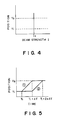
- the electron life is determined if the X-ray intensity is detected twice for one electron injection.
- three or more detections are performed at regular intervals for one electron injection, and the electron life is determined as an average or using least square approximation.
- the intensity is detected at such intervals that the X-ray intensity attenuates by a predetermined degree from the past data, and then the electron life ⁇ is correctly determined with small number of detections. For example, assuming that the electron life determined on the basis of the past data is ⁇ , and the detection is performed for every 5 % attenuation, the detection timing is 0.051 ⁇ , 0.105 ⁇ , 0.16 ⁇ and 0.22 ⁇ .
- the stage 313 is moved to place the illuminance measuring sensor 314 to a desired point in the exposure area, and the movable aperture 315 is moved as described in conjunction with Figures 17 - 21, by which the X-rays are projected onto the sensor 314.
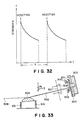
- Figure 33 shows another structure of the exposure apparatus to which an embodiment of the present invention is applicable. Since this embodiment is similar to Figure 27 embodiment, the same reference numerals as in Figure 27 are assigned to the elements having the corresponding functions, and the description thereof are omitted for simplicity.
- exposure apparatus uses a movable aperture 505 to limit the exposure amount, but in the apparatus of this embodiment, the mirror 509 is swung to control the exposure amount.
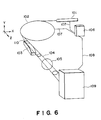
- the mirror 509 expands the SOR in the direction of the Y axis to illuminate a part of the mask 502 and a part of the wafer 501.
- the mirror 509 is swung by an actuator mechanism 531.
- the actuator mechanism 531 swings the mirror 509 in the direction y and in the direction Wx (x axis rotational direction).
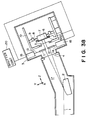
- Figure 38 shows a further embodiment.
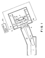
- the same reference numerals as in Figure 1 are assigned to the elements having the corresponding functions, and the detailed description of those elements are omitted for simplicity.
- the proper exposure period is 120 mJ/cm2
- the calculation is performed by the shutter controller 20.
- the aperture limiting or defining member 11 of the movable aperture stop 1 driven by the driver 15 for 121 sec from the time T1 to the time T2 at a speed of (Y2-Y1)/121 in the direction +Y, and thereafter, it is stopped.
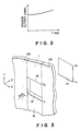
- (1) shows a relationship between a position of an edge surface 18 ( Figure 3) of the opening limiting member 11 of the movable aperture and the time.
- the opening limiting member 12 of the movable aperture stop is moved from the time T2 in the direction +Y by the driver 16.
- the shutter controller calculates the driving speed of the edge surface 19 to provide uniform amount of exposure within the angle of view 21 by the following equation:
- the amount of exposure within the view angle 21 is substantially uniformly 100 mJ/cm2.
- the detector 717 when the detector 717 is disposed in the orbit plane, it may be disposed in the vicinity of the X-ray mirror 703 as shown in Figure 44. As shown in Figure 43, it may be placed at a position A behind the X-ray mirror 703.
- the CPU unit 716 produces an exposure instruction and supply it to the shutter controller 715 by which the shutter driver 713 opens the shutter 707 to start the exposure. After start of the exposure operation, the shutter 707 is closed when the time period T elapses.
- the X-ray intensity attenuation during the exposure is deemed as being negligibly small.
- the CPU goes into the ending process sequence.
- the discrimination is made as to whether or not ⁇ (Ix/Ipo)Ip(t) (cumulative exposure amount) reaches the target exposure amount De, at step 727. If not, the operation returns, and if so, the interruption timer is deactuated. The shutter 707 is closed, and reset the current flag (ending process requiring flag) is reset, at step 728. Thus, the exposure operation is terminated.
- the detector 717 is not necessarily provided for each of the X-ray exposure apparatuses.
- the detector 717 is provided only for the exposure apparatus a
- the exposure apparatuses b - h are provided only with respective X-ray detectors 706 for detecting the X-ray intensity in the respective exposure areas
- the X-ray detectors 706 are advanced into the exposure areas in the respective exposure apparatuses a - h, and simultaneously with the detection of the X-ray intensity Ix, the output Ipo of the detector 717 is obtained in the apparatus a .
- the output Ipo of the detector 717 is transmitted through the communication path 731 to each of the exposure apparatuses a - h. Thereafter, the exposure intensity Ie of each of the apparatuses a - h is obtained from equation (7) on the basis of the output Ip(t) of the detector 717 during the exposure supplied through the communication path 731, the output Ipo and output Ix measured in each of the apparatuses a - h.
- An apparatus with which the detector 717 is provided, is not necessarily one of the exposure apparatuses.
Landscapes
- Physics & Mathematics (AREA)
- General Physics & Mathematics (AREA)
- Exposure Of Semiconductors, Excluding Electron Or Ion Beam Exposure (AREA)
- Exposure And Positioning Against Photoresist Photosensitive Materials (AREA)
Priority Applications (1)
| Application Number | Priority Date | Filing Date | Title |
|---|---|---|---|
| EP95202632A EP0694817B1 (de) | 1988-09-02 | 1989-08-31 | Belichtungsapparat |
Applications Claiming Priority (14)
| Application Number | Priority Date | Filing Date | Title |
|---|---|---|---|
| JP63218522A JP2700392B2 (ja) | 1988-09-02 | 1988-09-02 | 露光装置 |
| JP218522/88 | 1988-09-02 | ||
| JP63222253A JPH0271508A (ja) | 1988-09-07 | 1988-09-07 | 露光装置 |
| JP222251/88 | 1988-09-07 | ||
| JP222253/88 | 1988-09-07 | ||
| JP63222251A JP2750582B2 (ja) | 1988-09-07 | 1988-09-07 | X線露光方法 |
| JP63223483A JP2640247B2 (ja) | 1988-09-08 | 1988-09-08 | 露光装置 |
| JP223483/88 | 1988-09-08 | ||
| JP227389/88 | 1988-09-13 | ||
| JP63227388A JP2741039B2 (ja) | 1988-09-13 | 1988-09-13 | 露光装置 |
| JP63227389A JPH0276215A (ja) | 1988-09-13 | 1988-09-13 | 露光装置 |
| JP227388/88 | 1988-09-13 | ||
| JP133795/89 | 1989-05-26 | ||
| JP1133795A JP2877352B2 (ja) | 1989-05-26 | 1989-05-26 | X線露光装置 |
Related Child Applications (2)
| Application Number | Title | Priority Date | Filing Date |
|---|---|---|---|
| EP95202632.6 Division-Into | 1989-08-31 | ||
| EP95202632A Division EP0694817B1 (de) | 1988-09-02 | 1989-08-31 | Belichtungsapparat |
Publications (3)
| Publication Number | Publication Date |
|---|---|
| EP0357425A2 true EP0357425A2 (de) | 1990-03-07 |
| EP0357425A3 EP0357425A3 (de) | 1991-09-18 |
| EP0357425B1 EP0357425B1 (de) | 1996-11-06 |
Family
ID=27566014
Family Applications (2)
| Application Number | Title | Priority Date | Filing Date |
|---|---|---|---|
| EP89308823A Expired - Lifetime EP0357425B1 (de) | 1988-09-02 | 1989-08-31 | Belichtungseinrichtung |
| EP95202632A Expired - Lifetime EP0694817B1 (de) | 1988-09-02 | 1989-08-31 | Belichtungsapparat |
Family Applications After (1)
| Application Number | Title | Priority Date | Filing Date |
|---|---|---|---|
| EP95202632A Expired - Lifetime EP0694817B1 (de) | 1988-09-02 | 1989-08-31 | Belichtungsapparat |
Country Status (3)
| Country | Link |
|---|---|
| US (1) | US5157700A (de) |
| EP (2) | EP0357425B1 (de) |
| DE (2) | DE68929187T2 (de) |
Cited By (7)
| Publication number | Priority date | Publication date | Assignee | Title |
|---|---|---|---|---|
| EP0359370A3 (en) * | 1988-09-14 | 1990-11-14 | Canon Kabushiki Kaisha | Exposure control in x-ray exposure apparatus |
| EP0425739A1 (de) * | 1989-10-30 | 1991-05-08 | Canon Kabushiki Kaisha | Ausrichtevorrichtung und eine damit versehene Synchrotron-Röntgenbelichtungsvorrichtung |
| EP0446076A3 (en) * | 1990-03-09 | 1992-05-13 | Canon Kabushiki Kaisha | Exposure apparatus |
| EP0588579A1 (de) * | 1992-09-14 | 1994-03-23 | Canon Kabushiki Kaisha | Synchrotron-Röntgenbelichtungsverfahren |
| US5365561A (en) * | 1988-03-25 | 1994-11-15 | Canon Kabushiki Kaisha | Exposure control in an X-ray exposure apparatus |
| US5524131A (en) * | 1988-10-06 | 1996-06-04 | Canon Kabushiki Kaisha | Alignment apparatus and SOR x-ray exposure apparatus having same |
| EP1041444A3 (de) * | 1999-04-01 | 2004-05-06 | Sony Corporation | Vorrichtung und Verfahren zur Herstellung einer Halbleitervorrichtung |
Families Citing this family (27)
| Publication number | Priority date | Publication date | Assignee | Title |
|---|---|---|---|---|
| JP3025545B2 (ja) * | 1991-03-18 | 2000-03-27 | キヤノン株式会社 | X線リソグラフィ用マスクおよびx線リソグラフィ露光装置 |
| JP3049680B2 (ja) * | 1993-06-14 | 2000-06-05 | キヤノン株式会社 | ビーム位置検出装置及びこれを用いたシステム |
| JP3291408B2 (ja) * | 1994-04-04 | 2002-06-10 | キヤノン株式会社 | 露光装置および集積回路の製造方法 |
| US5835560A (en) * | 1994-05-24 | 1998-11-10 | Canon Kabushiki Kaisha | Exposure apparatus |
| JPH07321024A (ja) * | 1994-05-25 | 1995-12-08 | Canon Inc | 位置決め方法およびその装置ならびにこれらを用いた露光装置 |
| JP3391940B2 (ja) * | 1995-06-26 | 2003-03-31 | キヤノン株式会社 | 照明装置及び露光装置 |
| JP3666951B2 (ja) | 1995-10-06 | 2005-06-29 | キヤノン株式会社 | マーク検出方法、これを用いた位置合わせ方法、露光方法及び装置、ならびにデバイス生産方法 |
| US5920398A (en) * | 1996-03-01 | 1999-07-06 | Canon Kabushiki Kaisha | Surface position detecting method and scanning exposure method using the same |
| JP3862347B2 (ja) * | 1996-04-11 | 2006-12-27 | キヤノン株式会社 | X線縮小露光装置およびこれを利用したデバイス製造方法 |
| JP3284045B2 (ja) * | 1996-04-30 | 2002-05-20 | キヤノン株式会社 | X線光学装置およびデバイス製造方法 |
| US6559465B1 (en) | 1996-08-02 | 2003-05-06 | Canon Kabushiki Kaisha | Surface position detecting method having a detection timing determination |
| JP3337921B2 (ja) | 1996-08-23 | 2002-10-28 | キヤノン株式会社 | 投影露光装置および位置合せ方法 |
| KR0174997B1 (ko) * | 1996-12-20 | 1999-03-20 | 김광호 | 노광설비의 이중노광 방지장치 |
| JP3689516B2 (ja) * | 1997-01-29 | 2005-08-31 | キヤノン株式会社 | 電子ビーム露光装置 |
| US6484088B1 (en) * | 1999-05-04 | 2002-11-19 | Ssi Technologies, Inc. | Fuel optimization system with improved fuel level sensor |
| US6573732B1 (en) * | 1999-05-04 | 2003-06-03 | Ssi Technologies, Inc. | Dynamic range sensor and method of detecting near field echo signals |
| US6295332B1 (en) * | 1999-06-12 | 2001-09-25 | Robert Allen Selzer | Method of improving x-ray lithography in the sub 100nm range to create high quality semiconductor devices |
| JP2000357644A (ja) | 1999-06-14 | 2000-12-26 | Canon Inc | 露光方法及び露光装置 |
| JP2000357643A (ja) | 1999-06-14 | 2000-12-26 | Canon Inc | 露光方法及びそれを用いた露光装置 |
| US6954255B2 (en) * | 2001-06-15 | 2005-10-11 | Canon Kabushiki Kaisha | Exposure apparatus |
| US6934003B2 (en) * | 2002-01-07 | 2005-08-23 | Canon Kabushiki Kaisha | Exposure apparatus and device manufacturing method |
| JP2003297891A (ja) * | 2002-01-31 | 2003-10-17 | Rigaku Industrial Co | 半導体用蛍光x線分析装置 |
| US20070147579A1 (en) * | 2005-12-23 | 2007-06-28 | De Man Bruno K B | Method and system for radiographic imaging with organ-based radiation profile prescription |
| JP4789260B2 (ja) * | 2006-08-23 | 2011-10-12 | エスアイアイ・ナノテクノロジー株式会社 | 荷電粒子ビーム装置及びアパーチャの軸調整方法 |
| EP2461347A1 (de) | 2010-12-06 | 2012-06-06 | Fei Company | Detektorsystem für Transmissionselektronenmikroskop |
| DE102016220096B3 (de) * | 2016-10-14 | 2018-02-08 | Siemens Healthcare Gmbh | Verfahren zur Generierung von Röntgenbilddaten |
| US20180333657A1 (en) * | 2017-05-17 | 2018-11-22 | Sable Sand Solutions Inc. | Detection of contents of a sand separator using radiation |
Citations (10)
| Publication number | Priority date | Publication date | Assignee | Title |
|---|---|---|---|---|
| JPS5645026A (en) | 1979-09-20 | 1981-04-24 | Matsushita Electric Ind Co Ltd | Forming method for resin film on semiconductor substrate |
| JPS56104438A (en) | 1980-01-24 | 1981-08-20 | Rigaku Denki Kk | X-ray lithographic device |
| JPS57101839A (en) | 1980-12-18 | 1982-06-24 | Nippon Kogaku Kk <Nikon> | Exposure device for wafer or photomask |
| JPS59198726A (ja) | 1983-04-26 | 1984-11-10 | Fujitsu Ltd | Mic装置の製造方法 |
| JPS6084814A (ja) | 1983-06-22 | 1985-05-14 | Agency Of Ind Science & Technol | X線投射装置 |
| JPS60198726A (ja) | 1984-03-23 | 1985-10-08 | Hitachi Ltd | X線露光装置の露光量調整方法と装置 |
| JPS6159828A (ja) | 1984-08-31 | 1986-03-27 | Nippon Telegr & Teleph Corp <Ntt> | X線リソグラフイ装置 |
| JPS61113065A (ja) | 1984-11-07 | 1986-05-30 | Hitachi Ltd | 露光装置 |
| JPS61141135A (ja) | 1984-12-14 | 1986-06-28 | Hitachi Ltd | X線リソグラフイ装置 |
| JPS61276223A (ja) | 1985-05-30 | 1986-12-06 | Fujitsu Ltd | X線露光方法 |
Family Cites Families (7)
| Publication number | Priority date | Publication date | Assignee | Title |
|---|---|---|---|---|
| DE2722958A1 (de) * | 1977-05-20 | 1978-11-23 | Siemens Ag | Verfahren zur justierung einer halbleiterscheibe relativ zu einer bestrahlungsmaske bei der roentgenstrahl-fotolithografie |
| JPS57117238A (en) * | 1981-01-14 | 1982-07-21 | Nippon Kogaku Kk <Nikon> | Exposing and baking device for manufacturing integrated circuit with illuminometer |
| EP0083394B1 (de) * | 1981-12-31 | 1986-04-09 | International Business Machines Corporation | Verfahren und Vorrichtung für die gleichmässige Beleuchtung einer Fläche |
| JPS5952246A (ja) * | 1982-09-20 | 1984-03-26 | Nippon Kogaku Kk <Nikon> | 露光制御装置 |
| JPS6414918A (en) * | 1987-07-08 | 1989-01-19 | Nikon Corp | Stepper |
| AT393334B (de) * | 1988-01-22 | 1991-09-25 | Ims Ionen Mikrofab Syst | Anordnung zur stabilisierung einer bestrahlten maske |
| US4804978A (en) * | 1988-02-19 | 1989-02-14 | The Perkin-Elmer Corporation | Exposure control system for full field photolithography using pulsed sources |
-
1989
- 1989-08-31 EP EP89308823A patent/EP0357425B1/de not_active Expired - Lifetime
- 1989-08-31 EP EP95202632A patent/EP0694817B1/de not_active Expired - Lifetime
- 1989-08-31 US US07/401,615 patent/US5157700A/en not_active Expired - Fee Related
- 1989-08-31 DE DE68929187T patent/DE68929187T2/de not_active Expired - Fee Related
- 1989-08-31 DE DE68927430T patent/DE68927430T2/de not_active Expired - Fee Related
Patent Citations (10)
| Publication number | Priority date | Publication date | Assignee | Title |
|---|---|---|---|---|
| JPS5645026A (en) | 1979-09-20 | 1981-04-24 | Matsushita Electric Ind Co Ltd | Forming method for resin film on semiconductor substrate |
| JPS56104438A (en) | 1980-01-24 | 1981-08-20 | Rigaku Denki Kk | X-ray lithographic device |
| JPS57101839A (en) | 1980-12-18 | 1982-06-24 | Nippon Kogaku Kk <Nikon> | Exposure device for wafer or photomask |
| JPS59198726A (ja) | 1983-04-26 | 1984-11-10 | Fujitsu Ltd | Mic装置の製造方法 |
| JPS6084814A (ja) | 1983-06-22 | 1985-05-14 | Agency Of Ind Science & Technol | X線投射装置 |
| JPS60198726A (ja) | 1984-03-23 | 1985-10-08 | Hitachi Ltd | X線露光装置の露光量調整方法と装置 |
| JPS6159828A (ja) | 1984-08-31 | 1986-03-27 | Nippon Telegr & Teleph Corp <Ntt> | X線リソグラフイ装置 |
| JPS61113065A (ja) | 1984-11-07 | 1986-05-30 | Hitachi Ltd | 露光装置 |
| JPS61141135A (ja) | 1984-12-14 | 1986-06-28 | Hitachi Ltd | X線リソグラフイ装置 |
| JPS61276223A (ja) | 1985-05-30 | 1986-12-06 | Fujitsu Ltd | X線露光方法 |
Non-Patent Citations (4)
| Title |
|---|
| ACCELERATOR SCIENCE, vol. 12, no. 2, pages 95 |
| H. TANIO; K. HOH: "stationary large area exposure in synchrotron radiation lithography utilizing a new arrangement of magnets applied to the storage ring", JPN. APPL. PHYS., vol. 22, 1983, pages L718 - L720 |
| KOJI TANINO; OHTORI KOICHIRO: "Design of Stationary Toroidal Mirror for Large Area Synchrotron Radiation Exposure", 31TH APPLIED PHYSICS MEETING, 1984, pages 282 |
| KOJI TANINO; OHTORI KOICHIRO: "Design of Stationary Troidal Mirror for Large Area Synchrotron Radiation Exposure", 31TH APPLIED PHYSICS MEETING, 1984, pages 282 |
Cited By (11)
| Publication number | Priority date | Publication date | Assignee | Title |
|---|---|---|---|---|
| US5365561A (en) * | 1988-03-25 | 1994-11-15 | Canon Kabushiki Kaisha | Exposure control in an X-ray exposure apparatus |
| EP0359370A3 (en) * | 1988-09-14 | 1990-11-14 | Canon Kabushiki Kaisha | Exposure control in x-ray exposure apparatus |
| US5524131A (en) * | 1988-10-06 | 1996-06-04 | Canon Kabushiki Kaisha | Alignment apparatus and SOR x-ray exposure apparatus having same |
| US5822389A (en) * | 1988-10-06 | 1998-10-13 | Canon Kabushiki Kaisha | Alignment apparatus and SOR X-ray exposure apparatus having same |
| EP0425739A1 (de) * | 1989-10-30 | 1991-05-08 | Canon Kabushiki Kaisha | Ausrichtevorrichtung und eine damit versehene Synchrotron-Röntgenbelichtungsvorrichtung |
| EP0446076A3 (en) * | 1990-03-09 | 1992-05-13 | Canon Kabushiki Kaisha | Exposure apparatus |
| US5172402A (en) * | 1990-03-09 | 1992-12-15 | Canon Kabushiki Kaisha | Exposure apparatus |
| US5377251A (en) * | 1990-03-09 | 1994-12-27 | Canon Kabushiki Kaisha | Exposure apparatus |
| EP0588579A1 (de) * | 1992-09-14 | 1994-03-23 | Canon Kabushiki Kaisha | Synchrotron-Röntgenbelichtungsverfahren |
| US5606586A (en) * | 1992-09-14 | 1997-02-25 | Canon Kabushiki Kaisha | X-ray exposure method and apparatus and device manufacturing method |
| EP1041444A3 (de) * | 1999-04-01 | 2004-05-06 | Sony Corporation | Vorrichtung und Verfahren zur Herstellung einer Halbleitervorrichtung |
Also Published As
| Publication number | Publication date |
|---|---|
| DE68927430D1 (de) | 1996-12-12 |
| EP0694817A2 (de) | 1996-01-31 |
| EP0357425A3 (de) | 1991-09-18 |
| EP0357425B1 (de) | 1996-11-06 |
| EP0694817B1 (de) | 2000-03-22 |
| EP0694817A3 (de) | 1996-04-10 |
| DE68929187D1 (de) | 2000-04-27 |
| DE68927430T2 (de) | 1997-03-13 |
| DE68929187T2 (de) | 2000-09-28 |
| US5157700A (en) | 1992-10-20 |
Similar Documents
| Publication | Publication Date | Title |
|---|---|---|
| EP0694817B1 (de) | Belichtungsapparat | |
| KR101446820B1 (ko) | 마이크로리소그래피 투영 노광 장치의 조명 시스템 내의 다수의 미러 어레이들을 감시하는 방법 및 장치 | |
| US6317195B1 (en) | Projection exposure apparatus | |
| KR100545294B1 (ko) | 리소그래피 장치, 디바이스 제조방법, 성능측정방법,캘리브레이션 방법 및 컴퓨터 프로그램 | |
| US6721039B2 (en) | Exposure method, exposure apparatus and device producing method | |
| US4920505A (en) | Projection exposure apparatus | |
| US5831716A (en) | Slit-scanning type light exposure apparatus | |
| WO1998059364A1 (en) | Projection aligner, method of manufacturing the aligner, method of exposure using the aligner, and method of manufacturing circuit devices by using the aligner | |
| US6496247B2 (en) | Exposure apparatus and exposure method | |
| US4624551A (en) | Light irradiation control method for projection exposure apparatus | |
| US5131022A (en) | Exposure method and apparatus | |
| JP2001144004A (ja) | 露光方法、露光装置、及びデバイス製造方法 | |
| JPH11507146A (ja) | リソグラフィ走査露光投影装置 | |
| US5898480A (en) | Exposure method | |
| US5606586A (en) | X-ray exposure method and apparatus and device manufacturing method | |
| US6124064A (en) | Light exposure controlling method | |
| US5127029A (en) | X-ray exposure apparatus | |
| JP2744245B2 (ja) | 露光装置と露光方法 | |
| JP3282167B2 (ja) | 露光方法、走査型露光装置、及びデバイス製造方法 | |
| US8416389B2 (en) | Exposure apparatus and method of manufacturing device | |
| US6731377B2 (en) | Laser output control method, laser apparatus and exposure apparatus | |
| KR100588127B1 (ko) | 리소그래피장치, 디바이스제조방법 및 그것에 의하여제조된 디바이스 | |
| JPH09180993A (ja) | 露光装置及びデバイス製造方法 | |
| JP2741039B2 (ja) | 露光装置 | |
| JP2700392B2 (ja) | 露光装置 |
Legal Events
| Date | Code | Title | Description |
|---|---|---|---|
| PUAI | Public reference made under article 153(3) epc to a published international application that has entered the european phase |
Free format text: ORIGINAL CODE: 0009012 |
|
| AK | Designated contracting states |
Kind code of ref document: A2 Designated state(s): DE FR GB NL |
|
| 17P | Request for examination filed |
Effective date: 19901231 |
|
| PUAL | Search report despatched |
Free format text: ORIGINAL CODE: 0009013 |
|
| AK | Designated contracting states |
Kind code of ref document: A3 Designated state(s): DE FR GB NL |
|
| 17Q | First examination report despatched |
Effective date: 19931220 |
|
| GRAH | Despatch of communication of intention to grant a patent |
Free format text: ORIGINAL CODE: EPIDOS IGRA |
|
| GRAH | Despatch of communication of intention to grant a patent |
Free format text: ORIGINAL CODE: EPIDOS IGRA |
|
| GRAA | (expected) grant |
Free format text: ORIGINAL CODE: 0009210 |
|
| AK | Designated contracting states |
Kind code of ref document: B1 Designated state(s): DE FR GB NL |
|
| DX | Miscellaneous (deleted) | ||
| REF | Corresponds to: |
Ref document number: 68927430 Country of ref document: DE Date of ref document: 19961212 |
|
| ET | Fr: translation filed | ||
| RIN2 | Information on inventor provided after grant (corrected) |
Free format text: KUROSAWA, HIROSHI * AMEMIYA, MITSUAKI * TERASHIMA, SHIGERU * UDA, KOJI * SHIMODA, ISAMU * UZAWA, SHUNICHI * OZAWA, KUNITAKA * MORI, MAKIKO * EBINUMA, RYUICHI * HARA, SHINICHI * MIZUSAWA, NOBUTOSHI * KAWAKAMI, EIGO |
|
| RIN2 | Information on inventor provided after grant (corrected) |
Free format text: KUROSAWA, HIROSHI * AMEMIYA, MITSUAKI * TERASHIMA, SHIGERU * UDA, KOJI * SHIMODA, ISAMU * UZAWA, SHUNICHI * OZAWA, KUNITAKA * MORI, MAKIKO * EBINUMA, RYUICHI * HARA, SHINICHI * MIZUSAWA, NOBUTOSHI * KAWAKAMI, EIGO |
|
| PLBE | No opposition filed within time limit |
Free format text: ORIGINAL CODE: 0009261 |
|
| STAA | Information on the status of an ep patent application or granted ep patent |
Free format text: STATUS: NO OPPOSITION FILED WITHIN TIME LIMIT |
|
| 26N | No opposition filed | ||
| REG | Reference to a national code |
Ref country code: GB Ref legal event code: IF02 |
|
| PGFP | Annual fee paid to national office [announced via postgrant information from national office to epo] |
Ref country code: GB Payment date: 20030818 Year of fee payment: 15 |
|
| PGFP | Annual fee paid to national office [announced via postgrant information from national office to epo] |
Ref country code: FR Payment date: 20030828 Year of fee payment: 15 Ref country code: DE Payment date: 20030828 Year of fee payment: 15 |
|
| PGFP | Annual fee paid to national office [announced via postgrant information from national office to epo] |
Ref country code: NL Payment date: 20030831 Year of fee payment: 15 |
|
| PG25 | Lapsed in a contracting state [announced via postgrant information from national office to epo] |
Ref country code: GB Free format text: LAPSE BECAUSE OF NON-PAYMENT OF DUE FEES Effective date: 20040831 |
|
| PG25 | Lapsed in a contracting state [announced via postgrant information from national office to epo] |
Ref country code: NL Free format text: LAPSE BECAUSE OF NON-PAYMENT OF DUE FEES Effective date: 20050301 Ref country code: DE Free format text: LAPSE BECAUSE OF NON-PAYMENT OF DUE FEES Effective date: 20050301 |
|
| GBPC | Gb: european patent ceased through non-payment of renewal fee |
Effective date: 20040831 |
|
| PG25 | Lapsed in a contracting state [announced via postgrant information from national office to epo] |
Ref country code: FR Free format text: LAPSE BECAUSE OF NON-PAYMENT OF DUE FEES Effective date: 20050429 |
|
| NLV4 | Nl: lapsed or anulled due to non-payment of the annual fee |
Effective date: 20050301 |
|
| REG | Reference to a national code |
Ref country code: FR Ref legal event code: ST |