EP0358236B1 - Verfahren zur Messung der Periode eines Oberflächenfehlers - Google Patents
Verfahren zur Messung der Periode eines Oberflächenfehlers Download PDFInfo
- Publication number
- EP0358236B1 EP0358236B1 EP89116688A EP89116688A EP0358236B1 EP 0358236 B1 EP0358236 B1 EP 0358236B1 EP 89116688 A EP89116688 A EP 89116688A EP 89116688 A EP89116688 A EP 89116688A EP 0358236 B1 EP0358236 B1 EP 0358236B1
- Authority
- EP
- European Patent Office
- Prior art keywords
- period
- defects
- data
- base material
- web
- Prior art date
- Legal status (The legal status is an assumption and is not a legal conclusion. Google has not performed a legal analysis and makes no representation as to the accuracy of the status listed.)
- Expired - Lifetime
Links
- 230000007547 defect Effects 0.000 title claims description 70
- 238000000034 method Methods 0.000 title claims description 9
- 230000000737 periodic effect Effects 0.000 claims description 21
- 239000000463 material Substances 0.000 description 38
- 230000002950 deficient Effects 0.000 description 23
- 238000005259 measurement Methods 0.000 description 10
- 238000001514 detection method Methods 0.000 description 8
- 238000004519 manufacturing process Methods 0.000 description 4
- 229910052782 aluminium Inorganic materials 0.000 description 1
- XAGFODPZIPBFFR-UHFFFAOYSA-N aluminium Chemical compound [Al] XAGFODPZIPBFFR-UHFFFAOYSA-N 0.000 description 1
- 229910052751 metal Inorganic materials 0.000 description 1
- 239000002184 metal Substances 0.000 description 1
- 238000005498 polishing Methods 0.000 description 1
- 238000011045 prefiltration Methods 0.000 description 1
- 238000003908 quality control method Methods 0.000 description 1
- 238000000926 separation method Methods 0.000 description 1
Images


Classifications
-
- G—PHYSICS
- G01—MEASURING; TESTING
- G01N—INVESTIGATING OR ANALYSING MATERIALS BY DETERMINING THEIR CHEMICAL OR PHYSICAL PROPERTIES
- G01N21/00—Investigating or analysing materials by the use of optical means, i.e. using sub-millimetre waves, infrared, visible or ultraviolet light
- G01N21/84—Systems specially adapted for particular applications
- G01N21/88—Investigating the presence of flaws or contamination
- G01N21/89—Investigating the presence of flaws or contamination in moving material, e.g. running paper or textiles
- G01N21/892—Investigating the presence of flaws or contamination in moving material, e.g. running paper or textiles characterised by the flaw, defect or object feature examined
- G01N21/8922—Periodic flaws
-
- G—PHYSICS
- G01—MEASURING; TESTING
- G01N—INVESTIGATING OR ANALYSING MATERIALS BY DETERMINING THEIR CHEMICAL OR PHYSICAL PROPERTIES
- G01N21/00—Investigating or analysing materials by the use of optical means, i.e. using sub-millimetre waves, infrared, visible or ultraviolet light
- G01N21/84—Systems specially adapted for particular applications
- G01N21/88—Investigating the presence of flaws or contamination
- G01N21/8851—Scan or image signal processing specially adapted therefor, e.g. for scan signal adjustment, for detecting different kinds of defects, for compensating for structures, markings, edges
- G01N2021/8854—Grading and classifying of flaws
- G01N2021/8858—Flaw counting
-
- G—PHYSICS
- G01—MEASURING; TESTING
- G01N—INVESTIGATING OR ANALYSING MATERIALS BY DETERMINING THEIR CHEMICAL OR PHYSICAL PROPERTIES
- G01N21/00—Investigating or analysing materials by the use of optical means, i.e. using sub-millimetre waves, infrared, visible or ultraviolet light
- G01N21/84—Systems specially adapted for particular applications
- G01N21/88—Investigating the presence of flaws or contamination
- G01N21/89—Investigating the presence of flaws or contamination in moving material, e.g. running paper or textiles
- G01N2021/8909—Scan signal processing specially adapted for inspection of running sheets
- G01N2021/8912—Processing using lane subdivision
Definitions
- the present invention relates to a method of measuring a period on which a surface defect appears in a traveling web
- Such a surface inspecting apparatus is used to detect surface defects, such as scratches and pin holes, of a surface of a traveling web appearing not only at random but also periodically.
- surface defects are counted by opening a time gate at an elapse of a predetermined time period from a time a first surface defect is detected. After several times of this periodic detections, if more than a predetermined number of surface defects are detected every periodic detection, the web is estimated to have periodic surface defects.
- a flaw detection system for detecting repeating defects occurring in a web which is divided into lanes for processing purposes.
- the process for detecting flaws occurring in a single lane is explained.
- Upon the occurrence of a first flaw its position is stored in a prefilter section of a computer.
- When the next succeeding flaw occurs in that lane, its separation distance to the first flaw is compared with a predetermined list of repeat defect sizes. This list of repeat defect sizes corresponds to the circumstances of rollers which convey the web.
- a post filter shift register is created in the computer indicating that further processing is desirable.
- the post filter projects a location or a selected tolerance window from the measured distance where the next flaw or defect should occur if it repeats. Further projection of windows based on an initial match are continued by either the distance from the occurrence of the last flaw within the window or from the center of a projected window in the event of a miss If three or more out of five sequenced locations containing defects are detected, an alarm is generated which may be used to stop the rollers.
- a flaw detection system for sensing surface flaws generated by more than two rolls of different diameters.
- a detection signal generated by a photo detector is stored in a register and subsequently in an image memory.
- the contents of the image memory are processed with a multiplier, an adder, a further register for operated values and a comperator to which a set value is applied.
- the processing is carried out in a manner that the flaw detection signal is autocorrelated in real time.
- (d i ⁇ d i + j ) is a product of a binary data d i for an i-th data cell and a binary data d i + j for a (i + j)-th data cell. That is, the product is "1" only when both of the binary data d i and d i + j are "1" indicating both of the i-th data cell and (i + j)-th data cell are defective. Accordingly, the autocorrelation I expresses the number of pairs of defects at a regular distance of j for a data row consisting of binary data for the number of n data cells.
- a time required to perform the calculation is proportional to n ⁇ (n - 1). That is, multiplication and addition have to be repeated n ⁇ (n - 1) times for the number of n of data.
- the number n is a value of a length L of the web for measurement divided by a unit length s .
- Time necessary to perform calculation of elemental period of surface defects which depends upon given hardware and program, is heretofore long and a high processing capacity of computer or a special hardware is needed to perform such a calculation in a real time manner.
- the surface of the traveling web is divided into a number of data cells and data of each data cell is expressed by means of a binary data "1" indicating a defective surface or a binary data "0" indicating non-defective or normal surface.
- the periodicity of these surface defects is decided by the use of an autocorrelation expressing a frequency of appearance of these distances.
- the time needed to calculate a period of surface defect is greately shortened in comparison with a manner using an autocorrelation resulting from performing a multiplication and an addition for all of the binary data. Therefore, the measurement of a period of surface defect can be effected in a real time manner without using a large computer or a specially provided hardware.
- the measuring of the period of periodic defects is preferably effected every predetermined distance of movement of the web.
- FIG. 1 the method of measuring a period of surface defect according to a preferred embodiment of the present invention which is applied to a lithographic plate manufacturing line is shown.
- An aluminum web 3 (which is hereinafter referred to as a base material) from which lithographic plates are made is rolled on a reel 2.
- the base material 3 is continuously withdrawn and transported towards a processing apparatus 5 by means of a drive roller 4.
- the processing apparatus 5 is provided with rollers 6 for polishing surfaces of the base material 3 so as to make them smooth.
- the base material 3 thus smoothed is transported by means of drive rollers 8 and a guide roller 9 and wound around a reel 10.
- a flying spot type of surface scanning device which is disposed between the drive roller 8 and guide roller 9, consists of a scanner 12 and a light detector 13.
- the scanner 12 scans a surface of the base material 3 in a transverse direction perpendicular to the moving direction of the base material with a small diameter of flying spot.
- the light modulated by surface defect is reflected from the surface of the base material 3 and directed towards the light detector 13.
- the light detector 13 detects the modulated light to provide a surface signal.
- the scanner 12 scans the surface of the base material 3, it outputs scan signal to a lane data generator 14.
- the lane data generator 14 generates scanning lane signals SL indicating transverse positions or lanes of the surface of the base material 3 correspondingly to the surface signals from the detector 13.
- the scanning lane signals are sent to a binary signal generator 16.
- the light detector 13 extends in parallel to the transverse direction of the base material 3 to receive the light modulated by and reflected from surface defects of the base material 3. Accordingly, if the surface of the base material 3 has no surface defects, surface signals produced by the light detector 13 are at levels lower than a certain signal level. On the other hand, if the base material 3 has surface defects, the light detector 13 produces surface signals at levels greater than the certain signal level.
- a rotary encoder 17 is connected to the drive roller 8 to produce scanning cell position signals indicating cells on the base material 3 in the moving direction and send them to the binary signal generator 16.
- the surface signals are sent to a binary signal generating circuit 16 and converted to binary signals, "0" or “1", according to their signal levels thereby. That is, if a surface signal from the light detector 13 is at a signal level lower than the certain signal level, the binary signal generator 16 produces a binary signal of "0" indicating a standard or normal surface of the base material 3 (which is referred to as a standard surface) and if a surface signal SS from the light detector 13 is at a signal level greater than the certain signal level, the binary signal generator 16 produces a binary signal of "1" indicating a significant defective surface of the base material 3 (which is referred to as a defective surface).
- the binary signal BS is sent as a surface data signal to the data processing unit 15.
- Data processing unit 15 is connected to a data input unit 18, such as a keyboard, through which various data are input to set initial data necessary for measuring a period of surface defect.
- the initial data and the result of measurement are displayed on a display 19, such as a CRT and, if necessary, printed out by means of a printer 20.
- the display 19 and the printer 20 can be of any well known type and need not be described in detail herein.
- a length L of the base material 3 to be measured (which is referred to as a measuring length) is also initially set in accordance with a period of surface defect to be measured. It is to be noted in this embodiment that the measuring length L is set six times as long as an expected maximum period of surface defect.
- the surface scanning device is actuated to scan the surface of the base material 3.
- Surface signals SS from th-e light detector 13 of the surface scanning device are converted into binary signals BS; normal surface signals "0” or defective surface signals "1", which in turn are sent to the data processing unit 15.
- Fig. 2 conceptually showing a distribution of binary signals BS corresponding to data cells of the base material 3, the base material 3 of the measuring length L is divided into a number of lanes, #1, #2, #3, « (three of which are shown in Fig. 2) along the moving direction and each lane is divided into a number of, for example 29, data cells having a width of a unit distance s in the measuring length L. As shown, each data cell of the base material 3 is assigned one binary signal BS.
- a period of surface defect in the No. 1 lane #1 will be exemplarily described with reference to Fig. 2.
- Fig. 2 there are a number m of, for example 9, defective surface signals "1" in the No. 1 lane #1 in the measuring length L of the base material 3, which defective surface signals are correspondingly given to data of locations in the moving direction of cells having surface defects.
- a distance l ij between every two defective surface signals "1" which must be integral multiples of the width of s of a data cell, can be obtained.
- An autocorrelation AC(lij) which indicates a frequency at which two defective surface signals "1" at a same distance l ij appear, is given in accordance with the obtained distances l ij .
- a maximum time necessary to calculate the autocorrelation AC(l ij ) for the number of m of defective surface signals "1" is proportional to m (m - 1) and, therefore, has a correlation to the number of defective surface signals.
- the autocorrelation AC(l ij ) thus obtained is equivalent to the conventional autocorrelation AC(j) as was previously described.
- the periodicity of this autocorrelation AC(l ij ) is discriminated by the following conditions: AC(f 0 ) > 0 AND AC(2 ⁇ f 0 ) > 0 AND whil, AND AC(k ⁇ f 0 ) > 0 where k is a predetermined value for indicating a maximum times period component (k ⁇ f 0 ) of fundamental period f 0 for discriminating the periodicity of the autocorrelation AC(l ij ).
- the conditions are based on the fact that AC(l ij ) has a fundamental period component f 0 and 2 to k times period components of f 0 in the case that detected defects include periodic defects of period f 0 and the number of periodic defects is more than k. According to the conditions, a fundamental period f o is obtained.
- the maximum time is proportional to M max ⁇ (M max - 1).
- the maximum number M max of defective surface signals depends upon the minimum period X min of surface defect and the minimum period X min is determined approximately 10 times as long as a unit distance s in the consideration of resolution in measurement
- a distance calculation (a subtraction of integers) and a frequency calculation (an addition of integers) are repeated M max ⁇ (M max - 1) times.
- a necessary time for calculating the autocorrelation AC(l ij ) depends upon the number m of defective surface signals "1" included in the number n of binary signals BS, the usage of the autocorrelation AC(l ij ) develops one hundredth of the total calculation time as short as that achieved by the usage of the conventional autocorrelation AC(j) even in the case of the longest total calculation time.
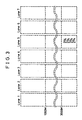
- Detection of periodic surface defects is performed in the above described manner. If periodic surface defects are detected, the printer 20 is actuated to print out data of the detected periodic surface defects as shown in Fig. 3.
- a period (mimimum period X min - maximum period X max ) and the unit distance s are set to 100-8472mm, and 15mm, respectively.
- the base material 3, which usually has a maximum width of approximately 1,500mm, is divided into 15 lanes having a width of 100mm so as to form data collecting areas of 15 x 100mm in the base material 3. Accordingly, 15 bits of binary data are collected every 15mm of movement of the base material 3.
- a measured result is output every 100m movement of the base material 3 as shown in Fig. 3. Because periodic surface defects of the base material 3 in the lithographic plate manufacturing line are often caused by surface irregularities of the rollers 4, 8, 9 and/or 6, the measured result is, in this example shown in Fig. 3, numerically indicated by a value of a measured period of surface defect divided by the ratio of the circumferential to the diameter of a roller. In Fig.
- the indication "274" indicates that the base material 3 has a periodic surface defect caused by a roller having a diameter of 274mm in the fifth lane (an area ranging from 400 to 500mm from the side edge of the base material 3) at a distance of 3000 to 3400m from the leading end of the base material 3.
Landscapes
- Engineering & Computer Science (AREA)
- Textile Engineering (AREA)
- Physics & Mathematics (AREA)
- Health & Medical Sciences (AREA)
- Life Sciences & Earth Sciences (AREA)
- Chemical & Material Sciences (AREA)
- Analytical Chemistry (AREA)
- Biochemistry (AREA)
- General Health & Medical Sciences (AREA)
- General Physics & Mathematics (AREA)
- Immunology (AREA)
- Pathology (AREA)
- Investigating Materials By The Use Of Optical Means Adapted For Particular Applications (AREA)
- Length Measuring Devices By Optical Means (AREA)
Claims (3)
- Ein Verfahren zum Messen der Periode f0 eines periodischen Defekts auf der Oberfläche eines Bandes, das sich in Längenrichtung bewegt, umfassend die Schritte:a) Erhalten einer Mehrzahl m an Defektsignalen, wobei jedes das Vorhandensein und die Position eines Defekts auf der Oberfläche, welche entlang einer vorbestimmten Länge (L) des Bandes in der Längsrichtung detektiert worden sind, repräsentiert;b) Erhalten von Abstandsdaten, welche den Abstand lij zwischen dem i-ten und j-ten detektierten Defekt für alle detektierten Defekte entlang der vorbestimmten Länge repräsentieren, wobei i = 1, 2, ..., m-1 und j = i+1, i+2, ..., m,c) Berechnen der Autokorrelation AC(lij), welche die Frequenz darstellt, mit der Paare von Defekten mit einem Abstand lij voneinander entfernt auftreten; undd) Bestimmen des Vorhandenseins und des Werts der Periode f0 eines periodischen Defekts, wobei die Periode identifiziert wird, wenn die folgende Bedingung erfüllt ist:

- Ein Verfahren nach Anspruch 1, in welchem das Messen der Periode f0 jeden vorbestimmten Abstand der Bewegung des Bands (3) ausgeführt wird.
- Ein Verfahren nach Anspruch 1 oder 2, in welchem das Messen der Periode f0 für eine Mehrzahl von Längsspuren ausgeführt wird, die eine vorbestimmte Breite aufweisen, in welche die Oberfläche des Bandes (3) geteilt worden ist.
Applications Claiming Priority (2)
| Application Number | Priority Date | Filing Date | Title |
|---|---|---|---|
| JP226190/88 | 1988-09-09 | ||
| JP63226190A JPH0786474B2 (ja) | 1988-09-09 | 1988-09-09 | 欠陥周期の測定方法 |
Publications (3)
| Publication Number | Publication Date |
|---|---|
| EP0358236A2 EP0358236A2 (de) | 1990-03-14 |
| EP0358236A3 EP0358236A3 (de) | 1991-05-29 |
| EP0358236B1 true EP0358236B1 (de) | 1997-12-29 |
Family
ID=16841298
Family Applications (1)
| Application Number | Title | Priority Date | Filing Date |
|---|---|---|---|
| EP89116688A Expired - Lifetime EP0358236B1 (de) | 1988-09-09 | 1989-09-08 | Verfahren zur Messung der Periode eines Oberflächenfehlers |
Country Status (4)
| Country | Link |
|---|---|
| US (1) | US4982600A (de) |
| EP (1) | EP0358236B1 (de) |
| JP (1) | JPH0786474B2 (de) |
| DE (1) | DE68928510T2 (de) |
Families Citing this family (30)
| Publication number | Priority date | Publication date | Assignee | Title |
|---|---|---|---|---|
| EP0475454A3 (en) * | 1990-09-14 | 1992-10-14 | Fuji Photo Film Co., Ltd. | Defect inspection system |
| JP2535257B2 (ja) * | 1991-05-07 | 1996-09-18 | 新日本製鐵株式会社 | ストリップの表面欠陥検査装置 |
| US5508622A (en) * | 1994-12-14 | 1996-04-16 | Gatzlaff; Harold | Coating defect detector system |
| US5678447A (en) * | 1996-04-17 | 1997-10-21 | Eastman Kodak Company | On-line web planarity measurement apparatus and method |
| FR2770646B1 (fr) * | 1997-11-06 | 1999-12-17 | Eastman Kodak Co | Procede d'identification de defauts d'une enduction |
| AU1353899A (en) * | 1997-11-27 | 1999-06-16 | Hoogovens Staal Bv | Process and device for producing a strip-like material avoiding repeated surfacedefects |
| EP0927887A1 (de) * | 1997-12-17 | 1999-07-07 | Zellweger Luwa Ag | Verfahren zur Erkennung periodischer Fehler in einem längsbewegten Prüfgut |
| US6895811B2 (en) * | 2001-12-14 | 2005-05-24 | Shawmut Corporation | Detection of small holes in laminates |
| US7623699B2 (en) * | 2004-04-19 | 2009-11-24 | 3M Innovative Properties Company | Apparatus and method for the automated marking of defects on webs of material |
| US7176475B2 (en) | 2004-11-16 | 2007-02-13 | Omron Corporation | Adjusting apparatus, production processing system, and method of controlling adjusting apparatus |
| US7748259B2 (en) * | 2006-12-15 | 2010-07-06 | General Electric Company | Systems and methods for solid oxide fuel cell surface analysis |
| US7542821B2 (en) * | 2007-07-26 | 2009-06-02 | 3M Innovative Properties Company | Multi-unit process spatial synchronization of image inspection systems |
| US20090028417A1 (en) * | 2007-07-26 | 2009-01-29 | 3M Innovative Properties Company | Fiducial marking for multi-unit process spatial synchronization |
| US8175739B2 (en) * | 2007-07-26 | 2012-05-08 | 3M Innovative Properties Company | Multi-unit process spatial synchronization |
| US7493678B1 (en) * | 2007-09-13 | 2009-02-24 | Ming-Tse Chen | Method of inspecting cloth |
| US7781622B2 (en) * | 2008-01-25 | 2010-08-24 | Council Of Scientific & Industrial Research | Process for direct hydroxylation of aromatic hydrocarbons |
| JP5453861B2 (ja) * | 2008-03-31 | 2014-03-26 | Jfeスチール株式会社 | 周期性欠陥検出装置及びその方法 |
| US7937233B2 (en) * | 2008-04-17 | 2011-05-03 | 3M Innovative Properties Company | Preferential defect marking on a web |
| KR101609007B1 (ko) * | 2008-07-18 | 2016-04-04 | 아사히 가라스 가부시키가이샤 | 결함 검사를 위한 화상 데이터의 처리 장치 및 방법, 이것들을 사용한 결함 검사 장치 및 방법, 이것들을 사용한 판 형상체의 제조 방법, 및 기록 매체 |
| US7797133B2 (en) * | 2008-09-10 | 2010-09-14 | 3M Innovative Properties Company | Multi-roller registered repeat defect detection of a web process line |
| KR100905519B1 (ko) * | 2009-03-11 | 2009-07-01 | 와이즈플래닛(주) | 비쥬얼 엔코더를 이용하여 컨베이어상에서 이동하는 패널의결함 위치 정합성을 제공하는 방법 |
| CN102792154B (zh) * | 2010-03-10 | 2015-09-23 | 3M创新有限公司 | 幅材制备工艺中专用的重复缺陷检测 |
| DE102011083405A1 (de) * | 2010-12-21 | 2012-06-21 | Sms Siemag Ag | Verfahren und Vorrichtung zur Oberflächeninspektion von Bandstücken |
| CN103507408A (zh) * | 2013-09-19 | 2014-01-15 | 安庆市康明纳包装有限公司 | 一种印刷机的自动检测装置 |
| JP6062396B2 (ja) * | 2014-06-16 | 2017-01-18 | Ckd株式会社 | 検査システム及びptp包装機 |
| DE102017108495B4 (de) * | 2017-04-21 | 2025-12-31 | Windmöller & Hölscher Kg | Überwachungsverfahren zur Überwachung eines Abwickelprozesses, Abwickelvorrichtung sowie Abwickelsystem |
| US10501274B2 (en) | 2017-07-06 | 2019-12-10 | Honeywell International Inc. | Continuous web sheet defect analytics, classification and remediation for enhancing equipment efficiency and throughput |
| US20230122383A1 (en) * | 2021-10-18 | 2023-04-20 | Edwin J. Lightfoot | Method and apparatus for the real time quantification of subtle variations in a planar material and identification of a corresponding source of the identified subtle variation |
| CN116148431B (zh) * | 2023-03-02 | 2025-08-05 | 北京首钢股份有限公司 | 带钢质量判断方法及装置 |
| JP7723785B1 (ja) * | 2024-03-25 | 2025-08-14 | Ckd株式会社 | シール手段異常検出システム及びブリスタ包装機 |
Family Cites Families (17)
| Publication number | Priority date | Publication date | Assignee | Title |
|---|---|---|---|---|
| FR1150424A (fr) * | 1956-05-03 | 1958-01-13 | Procédé et appareil pour le contrôle de l'irrégularité de courants de matières textiles ou similaires | |
| US3112642A (en) * | 1960-05-06 | 1963-12-03 | Republic Steel Corp | Apparatus for measuring surface roughness |
| US3971272A (en) * | 1963-10-01 | 1976-07-27 | Zellweger, Ltd. | Regulation of electronically operated quality control equipment |
| US3377828A (en) * | 1963-12-02 | 1968-04-16 | Republic Steel Corp | Method of rolling metal strip to control surface roughness |
| DE1245605B (de) * | 1964-10-20 | 1967-07-27 | Janez Peklenik Dr Ing | Verfahren und Vorrichtung zur Kenngroessenermittlung bei stochastischen Prozessen |
| GB1207241A (en) * | 1967-03-30 | 1970-09-30 | Sumitomo Metal Ind | Method of and apparatus for detecting local irregularities in strip and for controlling the evenness of strip |
| US3633211A (en) * | 1969-10-17 | 1972-01-04 | American Electronic Lab | Inspection recorder means |
| JPS4935091A (de) * | 1972-08-01 | 1974-04-01 | ||
| US3835332A (en) * | 1973-06-04 | 1974-09-10 | Eastman Kodak Co | Inspection apparatus for detecting defects in a web |
| JPS5112154A (en) * | 1974-07-22 | 1976-01-30 | Nippon Kokan Kk | Hyomenheitandosokuteihoho |
| DE2525560C2 (de) * | 1975-06-07 | 1991-04-18 | Fritz 7347 Bad Überkingen Stahlecker | Wartungseinrichtung die längs einer eine Vielzahl von nebeneinander angeordneten Spinnstellen aufweisenden Offenend-Spinnmaschine verfahrbar ist |
| DE2550814C3 (de) * | 1975-11-12 | 1979-08-09 | Erwin Sick Gmbh Optik-Elektronik, 7808 Waldkirch | Zeilentastvorrichtung für Materialbahnen zur Fehlstellenermittlung |
| US4134684A (en) * | 1977-01-18 | 1979-01-16 | Intex Corp. | Repeat defect detector system |
| US4348114A (en) * | 1979-12-07 | 1982-09-07 | Ciba-Geigy Ag | Method of inspecting coated web material to detect the presence of downlines thereon |
| SU939929A1 (ru) * | 1980-04-08 | 1982-06-30 | Калининский филиал Всесоюзного научно-исследовательского института вагоностроения | Устройство дл измерени волнистости |
| SE459013B (sv) * | 1987-09-22 | 1989-05-29 | Svenska Traeforskningsinst | Saett foer maetning av variationer i egenskaper hos en kontinuerligt loepande pappersbana |
| US4958307A (en) * | 1987-11-20 | 1990-09-18 | Kabushiki Kaisha Toshiba | Roll mark inspection apparatus |
-
1988
- 1988-09-09 JP JP63226190A patent/JPH0786474B2/ja not_active Expired - Fee Related
-
1989
- 1989-09-08 EP EP89116688A patent/EP0358236B1/de not_active Expired - Lifetime
- 1989-09-08 DE DE68928510T patent/DE68928510T2/de not_active Expired - Fee Related
- 1989-09-11 US US07/405,215 patent/US4982600A/en not_active Expired - Lifetime
Also Published As
| Publication number | Publication date |
|---|---|
| EP0358236A2 (de) | 1990-03-14 |
| EP0358236A3 (de) | 1991-05-29 |
| JPH0274852A (ja) | 1990-03-14 |
| DE68928510T2 (de) | 1998-04-16 |
| DE68928510D1 (de) | 1998-02-05 |
| JPH0786474B2 (ja) | 1995-09-20 |
| US4982600A (en) | 1991-01-08 |
Similar Documents
| Publication | Publication Date | Title |
|---|---|---|
| US4982600A (en) | Method of measuring the period of surface defects | |
| EP0594220B1 (de) | Gerät zur inspektion von Walzzeichen | |
| US4134684A (en) | Repeat defect detector system | |
| JPS62500959A (ja) | 紙葉の状態検知装置 | |
| EP0483362B1 (de) | Vorrichtung zur messung der blattlänge | |
| US4928257A (en) | Method and apparatus for monitoring the thickness profile of a strip | |
| US4110048A (en) | Method of and an apparatus for inspecting a traveling sheet material | |
| JP3845958B2 (ja) | 周期欠陥検出方法および装置 | |
| JPH09138200A (ja) | 帯状体の表面欠陥判定方法 | |
| JP4433824B2 (ja) | 周期性疵検出方法および装置 | |
| JPH061168B2 (ja) | 形状不良検出装置 | |
| JP2000283932A (ja) | 帯状体エッジ部の欠陥検出方法 | |
| US20250091833A1 (en) | Web position tracking | |
| JPS63222244A (ja) | 表面検査装置 | |
| US6304314B1 (en) | Determination of the speed of movement of an image-bearing sheet | |
| JPH04291138A (ja) | ストリップの有疵部マーキング装置 | |
| JPH10221059A (ja) | 長尺鋼材の表面疵検出方法 | |
| JP2000321214A (ja) | 欠陥検出方法および装置 | |
| JPH02298840A (ja) | 神経回路網による鋼板表面疵検査方法 | |
| JPS5936051A (ja) | 紙葉類の穴検知装置 | |
| JPS63172945A (ja) | 周期性欠陥弁別処理回路 | |
| JPH0619259B2 (ja) | 表面欠陥検査方法 | |
| JPH0531101B2 (de) | ||
| JPH09184812A (ja) | 欠陥検出方法 | |
| JPH04270908A (ja) | 熱延鋼板の平面形状測定方法 |
Legal Events
| Date | Code | Title | Description |
|---|---|---|---|
| PUAI | Public reference made under article 153(3) epc to a published international application that has entered the european phase |
Free format text: ORIGINAL CODE: 0009012 |
|
| AK | Designated contracting states |
Kind code of ref document: A2 Designated state(s): DE GB NL |
|
| PUAL | Search report despatched |
Free format text: ORIGINAL CODE: 0009013 |
|
| AK | Designated contracting states |
Kind code of ref document: A3 Designated state(s): DE GB NL |
|
| 17P | Request for examination filed |
Effective date: 19910718 |
|
| 17Q | First examination report despatched |
Effective date: 19940504 |
|
| GRAG | Despatch of communication of intention to grant |
Free format text: ORIGINAL CODE: EPIDOS AGRA |
|
| GRAH | Despatch of communication of intention to grant a patent |
Free format text: ORIGINAL CODE: EPIDOS IGRA |
|
| GRAH | Despatch of communication of intention to grant a patent |
Free format text: ORIGINAL CODE: EPIDOS IGRA |
|
| GRAA | (expected) grant |
Free format text: ORIGINAL CODE: 0009210 |
|
| AK | Designated contracting states |
Kind code of ref document: B1 Designated state(s): DE GB NL |
|
| PG25 | Lapsed in a contracting state [announced via postgrant information from national office to epo] |
Ref country code: NL Free format text: LAPSE BECAUSE OF FAILURE TO SUBMIT A TRANSLATION OF THE DESCRIPTION OR TO PAY THE FEE WITHIN THE PRESCRIBED TIME-LIMIT Effective date: 19971229 |
|
| REF | Corresponds to: |
Ref document number: 68928510 Country of ref document: DE Date of ref document: 19980205 |
|
| NLV1 | Nl: lapsed or annulled due to failure to fulfill the requirements of art. 29p and 29m of the patents act | ||
| PLBE | No opposition filed within time limit |
Free format text: ORIGINAL CODE: 0009261 |
|
| STAA | Information on the status of an ep patent application or granted ep patent |
Free format text: STATUS: NO OPPOSITION FILED WITHIN TIME LIMIT |
|
| 26N | No opposition filed | ||
| REG | Reference to a national code |
Ref country code: GB Ref legal event code: IF02 |
|
| PGFP | Annual fee paid to national office [announced via postgrant information from national office to epo] |
Ref country code: GB Payment date: 20040827 Year of fee payment: 16 |
|
| PGFP | Annual fee paid to national office [announced via postgrant information from national office to epo] |
Ref country code: DE Payment date: 20041027 Year of fee payment: 16 |
|
| PG25 | Lapsed in a contracting state [announced via postgrant information from national office to epo] |
Ref country code: GB Free format text: LAPSE BECAUSE OF NON-PAYMENT OF DUE FEES Effective date: 20050908 |
|
| PG25 | Lapsed in a contracting state [announced via postgrant information from national office to epo] |
Ref country code: DE Free format text: LAPSE BECAUSE OF NON-PAYMENT OF DUE FEES Effective date: 20060401 |
|
| GBPC | Gb: european patent ceased through non-payment of renewal fee |
Effective date: 20050908 |
|
| REG | Reference to a national code |
Ref country code: GB Ref legal event code: 732E |