EP0361078A2 - Méthode de fabrication d'un dispositif semi-conducteur comprenant des régions peu profondes fortement dopées - Google Patents
Méthode de fabrication d'un dispositif semi-conducteur comprenant des régions peu profondes fortement dopées Download PDFInfo
- Publication number
- EP0361078A2 EP0361078A2 EP89115513A EP89115513A EP0361078A2 EP 0361078 A2 EP0361078 A2 EP 0361078A2 EP 89115513 A EP89115513 A EP 89115513A EP 89115513 A EP89115513 A EP 89115513A EP 0361078 A2 EP0361078 A2 EP 0361078A2
- Authority
- EP
- European Patent Office
- Prior art keywords
- layer
- silicon layer
- substrate
- diffusion regions
- dopant
- Prior art date
- Legal status (The legal status is an assumption and is not a legal conclusion. Google has not performed a legal analysis and makes no representation as to the accuracy of the status listed.)
- Withdrawn
Links
Images


Classifications
-
- H—ELECTRICITY
- H10—SEMICONDUCTOR DEVICES; ELECTRIC SOLID-STATE DEVICES NOT OTHERWISE PROVIDED FOR
- H10D—INORGANIC ELECTRIC SEMICONDUCTOR DEVICES
- H10D30/00—Field-effect transistors [FET]
- H10D30/01—Manufacture or treatment
- H10D30/021—Manufacture or treatment of FETs having insulated gates [IGFET]
- H10D30/0223—Manufacture or treatment of FETs having insulated gates [IGFET] having source and drain regions or source and drain extensions self-aligned to sides of the gate
-
- H—ELECTRICITY
- H10—SEMICONDUCTOR DEVICES; ELECTRIC SOLID-STATE DEVICES NOT OTHERWISE PROVIDED FOR
- H10D—INORGANIC ELECTRIC SEMICONDUCTOR DEVICES
- H10D64/00—Electrodes of devices having potential barriers
- H10D64/01—Manufacture or treatment
- H10D64/011—Manufacture or treatment of electrodes ohmically coupled to a semiconductor
- H10D64/0111—Manufacture or treatment of electrodes ohmically coupled to a semiconductor to Group IV semiconductors
- H10D64/0113—Manufacture or treatment of electrodes ohmically coupled to a semiconductor to Group IV semiconductors the conductive layers comprising highly doped semiconductor materials, e.g. polysilicon layers or amorphous silicon layers
-
- H—ELECTRICITY
- H10—SEMICONDUCTOR DEVICES; ELECTRIC SOLID-STATE DEVICES NOT OTHERWISE PROVIDED FOR
- H10P—GENERIC PROCESSES OR APPARATUS FOR THE MANUFACTURE OR TREATMENT OF DEVICES COVERED BY CLASS H10
- H10P32/00—Diffusion of dopants within, into or out of wafers, substrates or parts of devices
- H10P32/10—Diffusion of dopants within, into or out of semiconductor bodies or layers
- H10P32/14—Diffusion of dopants within, into or out of semiconductor bodies or layers within a single semiconductor body or layer in a solid phase; between different semiconductor bodies or layers, both in a solid phase
- H10P32/1408—Diffusion of dopants within, into or out of semiconductor bodies or layers within a single semiconductor body or layer in a solid phase; between different semiconductor bodies or layers, both in a solid phase from or through or into an external applied layer, e.g. photoresist or nitride layers
- H10P32/1414—Diffusion of dopants within, into or out of semiconductor bodies or layers within a single semiconductor body or layer in a solid phase; between different semiconductor bodies or layers, both in a solid phase from or through or into an external applied layer, e.g. photoresist or nitride layers the applied layer being silicon, silicide or SIPOS, e.g. polysilicon or porous silicon
-
- H—ELECTRICITY
- H10—SEMICONDUCTOR DEVICES; ELECTRIC SOLID-STATE DEVICES NOT OTHERWISE PROVIDED FOR
- H10P—GENERIC PROCESSES OR APPARATUS FOR THE MANUFACTURE OR TREATMENT OF DEVICES COVERED BY CLASS H10
- H10P32/00—Diffusion of dopants within, into or out of wafers, substrates or parts of devices
- H10P32/10—Diffusion of dopants within, into or out of semiconductor bodies or layers
- H10P32/17—Diffusion of dopants within, into or out of semiconductor bodies or layers characterised by the semiconductor material
- H10P32/171—Diffusion of dopants within, into or out of semiconductor bodies or layers characterised by the semiconductor material being group IV material
Definitions
- the present invention relates to a method for forming a semiconductor device, such as a large scale integrated circuit (LSI), having a fine structure suitable for high density integration. Particularly, it relates to a method for forming a shallow and high concentration impurity region in the relevant semiconductor substrate of the device.
- LSI large scale integrated circuit
- Fig. 1 (a) is a schematic diagram A having a peak point Pa at a depth Xa, illustrating the distribution of the dopant concentration with respect to a single crystalline silicon substrate which is implanted with dopant normally incident on the surface of the substrate.
- the dopant concentration is taken on the coordinate and the depth from the surface is taken on the abscissa.
- the peak point Pa can be selectively varied by adjusting the associated accelerating energy.
- the channeling effect there is an effect known as "the channeling effect". Projected range distribution in a single crystalline body is quite different from those in an amorphous body under the same implantation condition. This is because of the possibility that incident ions can channel along open directions which appear when the incident ion beam is aligned with a low index crystallographic direction. The ions implanted into a single crystalline body are likely to be channeled, proceeding deeper in the body than in the amorphous body. In the diagram A of Fig. 1(a), therefore, the peak point Pa is followed by an elongated tail, which suggests that the direct ion implantation to a single crystalline silicon substrate is not suitable to form a shallow and high dopant concentration diffused region.
- a solid-to-solid thermal diffusion technology is utilized to form a shallow diffusion region in a semiconductor substrate.
- a dopant carrying layer is formed over the surface of the substrate corresponding to doped regions (impurity regions) of the relevant MOS FET.
- the layer for example, is a polycrystalline silicon layer (hereinafter, referred to as a polysilicon layer) containing dopant therein.
- the dopant is implanted into the polysilicon layer by employing an ion implanting method.
- the substrate is subject to a rapid thermal annealing (RTA), resulting in thermal diffusion of dopant contained in the polysilicon layer into the substrate through the interface surface between the polysilicon layer and the substrate.
- RTA rapid thermal annealing
- Fig. 1 (b) is a schematic diagram, illustrating the distribution of the dopant concentration with respect to the above-described structure composed of the polysilicon layer and the single crystalline silicon substrate which are implanted with dopant.
- the diagram B represents the dopant concentration distribution when the dopant is implanted with an accelerating energy such that the peak point Pb is located approximately at the mid point Xb of the depth of the polysilicon layer, while the diagram C represents when the dopant is accelerated with higher energy with the result that the peak point pc is shifted to a depth Xc substantially near the interface F.
- the dopant concentration at the interface F of the diagram C is much higher than that of the diagram B.
- the dopant concentration of the doped polysilicon layer at the interface F is desirably as high as possible.
- the peak point of the concentration distribution of the dopant is desirable to be located as close as possible to the interface.
- the curve C is more preferable than the curve D.
- the depth X of the peak point P of the distribution is limited because dopant ions once penetrating the polysilicon layer and intruding into the single crystalline silicon substrate, can easily proceed further due to the channneling effect as clearly shown in Fig. 1(b), resulting in forming an undesirably deep dopant region in the substrate.
- the reduced depth and the high dopant concentrations are incompatible, providing a problem which must be solved.
- Fig. 2 (a) to (c) illustrate one example of a prior art methods for fabricating a metal-oxide field - effect transistor (MOS FET) having shallow source and drain regions (diffused regions) and contact layers connected to the source and drain regions with low contact resistance.
- MOS FET metal-oxide field - effect transistor
- a field insulating layer 2 is selectively formed on a silicon substrate 1 of p-type, doped with boron (B) for example, employing a conventional LOCOS (Local Oxidation of Silicon) method, having a window 8, through which the surface of the silicon substrate 1 is exposed.
- the window 8 is selectively formed corresponding to a diffusion region.
- a gate electrode 4 is formed on the silicon substrate 1 through a gate insulator 3. Then, the gate electrode 4 is surrounded by an insulating layer 5.
- Both of the insulating layer 5 and the field insulating layer 2 are made of silicon dioxide (SiO2).
- a polysilicon layer 6 is formed by a CVD (Chemical Vapor Deposition) method over the entire surface of the substrate 1, and phosphorus (P) ions are implanted downwardly to the surface of the substrate 1 to dope the polysilicon layer 6 in the n-type.
- the ions are distributed within the polysilicon layer 6. A part of the ions intrude into the upper portion of the substrate 1 passing through the polysilicon layer 6.
- the polysilicon layer 6 is patterned using a photolithographic-process such that the doped polysilicon layer 6 remains selectively at least over the window 8, namely over the predetermined source-drain regions.
- the substrate 1 is subject to a heating process to activate the phosphorus (P) ions, to diffuse the phosphorus (P) ions from the doped polysilicon layer 6 to the silicon substrate 1 of p-type with the result that shallow source and drain regions 7 of n-type are formed in the substrate 1 beneath the polysilicon layer 6.
- the dopant concentration distribution along the depth direction of the polysilicon layer 6 and the substrate 1 is also represented in Fig. 1(b). A reduced thickness of the doped regions is difficult to be realized due to the channeling effect as described above.
- An object of the present invention is to provide a method for fabricating a semiconductor device having physical dimensions of sub-micron order.
- Another object of the present invention is to provide a method for fabricating a dopant diffusion region having a reduced depth, high dopant concentration, and a high diffusion conductance.
- Still another object of the present invention is to provide a method for fabricating an MOS FET having dopant diffusion region with a reduced depth, high dopant concentration, a high diffusion conductance, and a substantially low contact resistance to the associated contact terminal.
- Further object of the present invention is to eliminate the defects of the prior art method that implanted dopant ions tend to proceed deep in a single crystalline semiconductor substrate hindering the realization of a shallow doped region due to the channeling effect.
- a method in which an amorphized silicon layer portion is formed in a single crystalline silicon substrate by implanting ions of silicon or germanium, for example, in a portion beneath the top surface of the substrate, and a polysilicon layer of a doped metal silicide layer, is formed over the amorphized silicon layer portion.
- the polysilicon layer is doped by ion implantation of dopant.
- the dopant ions are suppressed to intrude the underlying single crystalline silicon substrate.
- the dopant ions escape from the undesirable channeling effect.
- the substrate is subjected to a rapid thermal annealing.
- the dopant contained in the doped polysilicon layer or a doped metal silicide layer is thermally diffused into the amorphous silicon layer and simultaneously the amorphous silicon layer is converted to a single crystalline silicon layer by the heat treatment.
- the dopants are activated, being not able to diffuse into the substrate passing through the relevant field insulator and gate insulator.
- the contact resistance between both layers is substantially low.
- the dopant ions in the amorphized silicon layer portion are mostly activated therein, and do not go further into the underlying silicon substrate by the heat treatment so that the depth of the diffusion layer is approximately limited within the amorphized layer portion of the substrate. As the result, a shallow and highly concentration dense impurity material layer is formed.
- the temperature of the associated heat treatment can be selected favorably low, which leads to various fabricating advantages.
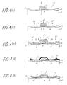
- Figs. from 3 (a) to 3(d) are cross-sectional views illustrating the fabricating steps of a first embodiment according to the present invention, presented in series.
- a single crystalline silicon substrate 1 of p-type, doped with boron (B) of the concentration of 1015/cm3 is prepared.
- a field insulating layer 2 having a window 8 is formed over the surface of the substrate using a conventional method.
- a gate electrode 4 is formed on the surface of the substrate 1 exposed through the window through a gate insulator 3, being surrounded by an insulating film 5 made of silicon dioxide (SiO2).
- the forming methods employed are the known ones.
- a layer portion beneath the exposed surface of the substrate 1 is amorphized by downwardly implanting silicon (Si) ions to the surface of the substrate 1.
- the ions are implanted through the window 8 except for the portion covered by the insulating film 5 under a condition, for example, of an accelerating energy of 40 KeV, and the dose of 4x10¹⁵/cm2.
- An amorphous silicon layer 10 is thus formed beneath the surface of the substrate 1, having a thickness of approximately 300 to 1000 Angstrom.
- the implanting condition is of an accelerating energy of 70 KeV and the dose of 4x10¹⁵/cm2.
- the polysilicon layer 6 is patterned by a conventional photolithographic process such that the doped polysilicon layer 6 is selectively left over the predetermined source and drain regions, namely over the windows 8.
- the substrate 1 is subject to a conventional rapid thermal annealing (RTA) method and heated an 1000 centigrade for 10 seconds.
- RTA rapid thermal annealing
- the implanted phosphorus (P) ions are activated, being diffused from the polysilicon layer 6 into the underlying amorphous silicon layer 10 which is simultaneously recrystallized and converted to a single crystalline silicon layer. Consequently, n-type source and drain regions 17 are formed.
- source and drain regions 17 are shallow diffusion layers with high dopant concentration. The depth of the regions is approximately 600 Angstrom, and the dopant concentration near the interface is approximately 1020/cm3.
- the doped polysilicon layer is formed by ion implanting of the relevant dopant to the polysilicon layer 6.
- the dopant concentration distribution is represented by the diagram D shown in Fig. 1(c).
- the accelerating energy of the dopant ion implantation is selected considering the thickness of the polysilicon layer 6 such that the peak point Pd is located substantially near the interface F.
- the implanted dopant ions go into the amorphized layer 10, being suppressed to proceed further because of the amorphized structure of the layer 10.
- the intrusion of the ions into the underlying single crystalline silicon substrate 1 is thus prevented, and the ions are escaped from the channeling effect.
- the dopant concentration diagram D is rapidly falling down in the amorphized layer 10.
- the diffusion region 17 formed by the subsequent RTA has a reduced depth almost limited within the amorphized layer 10, and the dopant concentration thereof is favorably high since the dopants in the region 17 are supplied from the doped polysilicon layer 6 by thermal diffusion and the dopant ions contained in the polysilicon layer, being added the dopant ions contained in the amorphized layer portion 10.
- the contact resistance between the polysilicon layer 6 and the diffusion layer 17 is substan tially low, since the dopant concentration near the interface between both layers is high.
- the temperature of the associated heat treatment can be favorably low, leading to various fabricating advantages.
- the doped polycristalline layer 6 functions as a contact terminal to each diffusion region 17 since the layer 6 has a favorable electrical conductivity.
- the electrical conductivity can be enhanced by converting the polysilicon layer 6 to a silicide layer, the method of which is disclosed next.
- a field insulating layer 2 having a window 8 is selectively formed over the surface of a silicon substrate 1 of p-type, doped with boron (B) of the concentration of 1015/cm3, employing a conventional method. Then, a gate electrode 4 is formed through a gate insulator 3 on the surface of the substrate exposed through the window 8, being surrounded by an insulating film 6.
- the ions are implanted under the conditions, for example, of a accelerating energy of 40 KeV, and the dose of 4x10¹⁵/cm2.
- the implanting condition is of an accelerating energy of 70 KeV, and the dose of 4x10¹⁵/cm2.
- the polysilicon layer 6 is patterned by a conventional photolithographic process such that the doped polysilicon layer 6 is selectively remained over at least the predetermined source-drain regions, namely diffusion regions. Subsequently, a titanium (Ti) film 11 is formed thereon employing a conventional sputtering method.
- Ti titanium
- a rapid heat treatment using a halogen lamp with a temperature rise of approximately 650 centigrade for 1 minute, the polysilicon layer 6 and the titanium (Ti) film 11 formed thereon, chemically react with each other, forming a titanium silicide layer 12. While the titanium (Ti) film 11 formed over the field insulating oxide layer 2 does not react with each other. The remaining titanium (Ti) film 11 is selectively removed with a usual chemical etching process using acids. After the removal, the substrate is heated at 750 centigrade for 30 seconds.
- RTA rapid heat treatment
- the doped phosphorus (P) ions are diffused from the polysilicon layer 6 into the underlying amorphous silicon layer portion 10, which is simultaneously recrystallized and converted to a single crystalline silicon layer, and the phosphorus (P) ions are activated at the same time.
- n-type source and drain regions 17 having a reduced depth, such as approximately 600 Angstrom, and high dopant concentration of approximately 1020/cm3 almost in the recrystallized layer portion 10.
- the formation of the titanium silicide film 12 and that of the diffused regions (source and drain regions 17) are performed simultaneously.
- a silicide layer is formed first employing a CVD method, and then the phosphorus (P) ions are implanted into the silicide layer to dope the silicide layer. Thereafter, the phosphorous (p) ions are diffused into the amorphous silicon layer 10.
- a platinum silicide layer other than the titanium silicide layer, a platinum silicide layer, a cobalt silicide layer, a tungsten silicide layer, a molybdenum silicide layer, a hafnium silicide layer, a vanadium silicide layer, and a zirconium silicide layer are applicable as a metal silicide layer.
- a dopant material except for phosphorus (P) arsenic (As) is applicable, and as a p-type dopant, boron (B) and boron fluoride (BF2) are applicable.
- the amorphous silicon layer portion is formed by ion planting the surface of the substrate 1. While, an amorphous silicon layer can be formed using a CVD method over the surface of the substrate before or after the formation of the field insulating layer 2. Furthermore, the polysilicon layer 6 may be doped to some degree in advance before the subsequent dopant ion implantation shown in Fig. 3(c) or Fig. 4(c). The preliminary doping of the polysilicon layer 6 is advantageous to reduce doping amount of the following ion implantation.
- the structure of an MOS transistor can be miniaturized and a short channel effect of the transistor is reduced, resulting in substantially improving the function and reliability of the transistor.
- the present invention is further applicable to the improvement of a bipolar transistor by miniaturizing the emitter contact thereof. Furthermore, in the above description, a doped silicon substrate or silicon layers are mentioned. However, it is apparent for the skilled person in the art, that the present invention is applic severelyable to the fabrication of another semiconductor device such as a gallium-arsenic (GaAs) transistor.
- GaAs gallium-arsenic
- the contact resistance and the diffusion resistance of the relevant dopant regions can be reduced and the physical dimensions, particularly the depth of the dopant region is favorably reduced.
- the present invention can effectively contribute to the miniaturization and the improvement of the function of the associated transistor.
Landscapes
- Insulated Gate Type Field-Effect Transistor (AREA)
- Electrodes Of Semiconductors (AREA)
Applications Claiming Priority (2)
| Application Number | Priority Date | Filing Date | Title |
|---|---|---|---|
| JP245569/88 | 1988-09-28 | ||
| JP63245569A JPH0291932A (ja) | 1988-09-28 | 1988-09-28 | 半導体装置の製造方法 |
Publications (2)
| Publication Number | Publication Date |
|---|---|
| EP0361078A2 true EP0361078A2 (fr) | 1990-04-04 |
| EP0361078A3 EP0361078A3 (fr) | 1990-04-25 |
Family
ID=17135668
Family Applications (1)
| Application Number | Title | Priority Date | Filing Date |
|---|---|---|---|
| EP89115513A Withdrawn EP0361078A3 (fr) | 1988-09-28 | 1989-08-23 | Méthode de fabrication d'un dispositif semi-conducteur comprenant des régions peu profondes fortement dopées |
Country Status (3)
| Country | Link |
|---|---|
| EP (1) | EP0361078A3 (fr) |
| JP (1) | JPH0291932A (fr) |
| KR (1) | KR920006850B1 (fr) |
Cited By (2)
| Publication number | Priority date | Publication date | Assignee | Title |
|---|---|---|---|---|
| WO2007105157A3 (fr) * | 2006-03-14 | 2007-11-15 | Nxp Bv | Formation de sources et de drains |
| US7622343B2 (en) | 1992-10-30 | 2009-11-24 | Semiconductor Energy Laboratory Co., Ltd. | Laser processing method, method for forming a flash memory, insulated gate semiconductor device and method for forming the same |
Families Citing this family (3)
| Publication number | Priority date | Publication date | Assignee | Title |
|---|---|---|---|---|
| JP2833468B2 (ja) * | 1994-02-17 | 1998-12-09 | 日本電気株式会社 | 半導体装置の製造方法 |
| JP2978736B2 (ja) * | 1994-06-21 | 1999-11-15 | 日本電気株式会社 | 半導体装置の製造方法 |
| JP5700025B2 (ja) * | 2012-11-27 | 2015-04-15 | トヨタ自動車株式会社 | 半導体装置とその製造方法 |
Family Cites Families (6)
| Publication number | Priority date | Publication date | Assignee | Title |
|---|---|---|---|---|
| JPS5853757B2 (ja) * | 1976-10-12 | 1983-12-01 | 原子能委員会核能研究所 | 原子炉 |
| JPS58161344A (ja) * | 1982-03-19 | 1983-09-24 | Oki Electric Ind Co Ltd | 半導体装置の製造方法 |
| JPS618916A (ja) * | 1984-06-21 | 1986-01-16 | インタ−ナシヨナル・ビジネス・マシ−ンズ・コ−ポレ−シヨン | ド−プ領域の形成方法 |
| JPS62130519A (ja) * | 1985-12-03 | 1987-06-12 | Sony Corp | 半導体薄膜への不純物ド−ピング方法 |
| IT1209682B (it) * | 1985-12-23 | 1989-08-30 | Sgs Microelettronica Spa | Processo per la fabbricazione mediante ricristallizzazione epitassiale di transistori ad effetto di campo a gate isolato con giunzioni a profondita' minima. |
| JPS62266829A (ja) * | 1986-05-14 | 1987-11-19 | Sharp Corp | 浅い接合層の形成方法 |
-
1988
- 1988-09-28 JP JP63245569A patent/JPH0291932A/ja active Pending
-
1989
- 1989-08-23 EP EP89115513A patent/EP0361078A3/fr not_active Withdrawn
- 1989-09-27 KR KR1019890013897A patent/KR920006850B1/ko not_active Expired
Cited By (2)
| Publication number | Priority date | Publication date | Assignee | Title |
|---|---|---|---|---|
| US7622343B2 (en) | 1992-10-30 | 2009-11-24 | Semiconductor Energy Laboratory Co., Ltd. | Laser processing method, method for forming a flash memory, insulated gate semiconductor device and method for forming the same |
| WO2007105157A3 (fr) * | 2006-03-14 | 2007-11-15 | Nxp Bv | Formation de sources et de drains |
Also Published As
| Publication number | Publication date |
|---|---|
| KR900005575A (ko) | 1990-04-14 |
| EP0361078A3 (fr) | 1990-04-25 |
| KR920006850B1 (ko) | 1992-08-20 |
| JPH0291932A (ja) | 1990-03-30 |
Similar Documents
| Publication | Publication Date | Title |
|---|---|---|
| US5006476A (en) | Transistor manufacturing process using three-step base doping | |
| JP3211394B2 (ja) | 半導体装置の製造方法 | |
| US8236675B2 (en) | Semiconductor device and method of fabricating a semiconductor device | |
| US5079182A (en) | Bicmos device having self-aligned well tap and method of fabrication | |
| KR100822228B1 (ko) | 반도체 장치 및 그 제조 방법 | |
| EP0137645B1 (fr) | Procédé de formation d'une région peu profonde du type N | |
| US5536676A (en) | Low temperature formation of silicided shallow junctions by ion implantation into thin silicon films | |
| JPH04226022A (ja) | 半導体構成体におけるスペーサの形成 | |
| JPS6379368A (ja) | ポリシリコンエミッタ及びシリサイド化ベ−スを持った高性能BiCMOS構成体の製造方法 | |
| US6130144A (en) | Method for making very shallow junctions in silicon devices | |
| US5593923A (en) | Method of fabricating semiconductor device having refractory metal silicide layer on impurity region using damage implant and single step anneal | |
| US4408387A (en) | Method for producing a bipolar transistor utilizing an oxidized semiconductor masking layer in conjunction with an anti-oxidation mask | |
| EP0401786B1 (fr) | Méthode de fabrication d'un transistor bipolaire latéral | |
| JPH04226064A (ja) | 半導体装置用の相互接続体及びその製造方法 | |
| US5443994A (en) | Method of fabricating a semiconductor device having a borosilicate glass spacer | |
| US5234847A (en) | Method of fabricating a BiCMOS device having closely spaced contacts | |
| EP0274217A1 (fr) | Procédé de fabrication d'un dispositif semi-conducteur | |
| EP0361078A2 (fr) | Méthode de fabrication d'un dispositif semi-conducteur comprenant des régions peu profondes fortement dopées | |
| EP0325181B1 (fr) | Procédé pour fabriquer un émetteur en polysilicium et une grille en polysilicium utilisant la même gravure de polysilicium sur un oxyde à grille mince | |
| JPH0878674A (ja) | 半導体装置およびその製造方法ならびにバイポーラトランジスタ | |
| JP2001007325A (ja) | 電界効果型トランジスタ | |
| US5405789A (en) | Method of manufacturing a semiconductor device whereby a laterally bounded semiconductor zone is formed in a semiconductor body in a self-aligning manner | |
| JPH05304158A (ja) | 半導体装置およびその製造方法 | |
| JP2000058822A (ja) | 半導体装置の製造方法 | |
| JPH1131665A (ja) | 半導体集積回路装置の製造方法 |
Legal Events
| Date | Code | Title | Description |
|---|---|---|---|
| PUAI | Public reference made under article 153(3) epc to a published international application that has entered the european phase |
Free format text: ORIGINAL CODE: 0009012 |
|
| PUAL | Search report despatched |
Free format text: ORIGINAL CODE: 0009013 |
|
| AK | Designated contracting states |
Kind code of ref document: A2 Designated state(s): DE FR GB |
|
| AK | Designated contracting states |
Kind code of ref document: A3 Designated state(s): DE FR GB |
|
| 17P | Request for examination filed |
Effective date: 19900510 |
|
| 17Q | First examination report despatched |
Effective date: 19921028 |
|
| STAA | Information on the status of an ep patent application or granted ep patent |
Free format text: STATUS: THE APPLICATION HAS BEEN WITHDRAWN |
|
| 18W | Application withdrawn |
Withdrawal date: 19930217 |