EP0362403A1 - Procede de sauvegarde d'un programme systeme - Google Patents
Procede de sauvegarde d'un programme systeme Download PDFInfo
- Publication number
- EP0362403A1 EP0362403A1 EP89903257A EP89903257A EP0362403A1 EP 0362403 A1 EP0362403 A1 EP 0362403A1 EP 89903257 A EP89903257 A EP 89903257A EP 89903257 A EP89903257 A EP 89903257A EP 0362403 A1 EP0362403 A1 EP 0362403A1
- Authority
- EP
- European Patent Office
- Prior art keywords
- cpu
- program
- supplementary
- system program
- saving
- Prior art date
- Legal status (The legal status is an assumption and is not a legal conclusion. Google has not performed a legal analysis and makes no representation as to the accuracy of the status listed.)
- Withdrawn
Links
Images




Classifications
-
- G—PHYSICS
- G06—COMPUTING OR CALCULATING; COUNTING
- G06F—ELECTRIC DIGITAL DATA PROCESSING
- G06F11/00—Error detection; Error correction; Monitoring
- G06F11/07—Responding to the occurrence of a fault, e.g. fault tolerance
- G06F11/14—Error detection or correction of the data by redundancy in operations
-
- G—PHYSICS
- G06—COMPUTING OR CALCULATING; COUNTING
- G06F—ELECTRIC DIGITAL DATA PROCESSING
- G06F11/00—Error detection; Error correction; Monitoring
- G06F11/07—Responding to the occurrence of a fault, e.g. fault tolerance
- G06F11/14—Error detection or correction of the data by redundancy in operations
- G06F11/1402—Saving, restoring, recovering or retrying
- G06F11/1415—Saving, restoring, recovering or retrying at system level
- G06F11/1441—Resetting or repowering
Definitions
- This invention relates to a method of saving a system program and, more particularly, to a method of saving, in an external memory device, the system program of each processor in a system comprising a plurality of processors.
- Fig. 7 is a block diagram of a system which adopts this proposed method.
- numeral 11 denotes an existing system (main system) of a computer configuration, the system including a processor (CPU) 11a, a ROM 11b in which an initializing program PLD M is stored, a RAM 11c, a keyboard 11d, a display unit 11e, an external memory device 11f equipped with a disk controller DKC, a floppy disk (FD) and the like, and a DI/DO circuit 11g.
- Stored on the FD are system programs SPR M , SPR S for the main system and a supplementary CPU, and an initializing program PLD S for the supplementary CPU.
- Numeral 12 denotes a separate CPU board, which includes a separate CPU board processor (CPU) 12a, and a DI/DO circuit 12c.
- Numeral 13 designates a common RAM provided so as to be accessible by both the CPU 11a of the main system and the supplementary CPU 12a. WKS represents a wake-up signal.
- the common RAM 13 serves also as the ROM of the supplementary CPU.
- a saving program contained in the system program SPR M of the main system 11 responds to a save request from the keyboard lid or the like by first saving its own system program SPR M in the external memory device 11f and then saving the supplementary CPU system program SPR s , which is in the common RAM 13, in the external memory device llf.
- the supplementary CPU board need not be provided with a ROM.
- Another problem is that the size of the RAM on the side of the supplementary CPU 12 is limited to the size of the common RAM.
- an object of the present invention is to provide a system program saving method in which a supplementary CPU need not be provided with a ROM.
- Another object of the present invention is to provide a system program saving method in which it is unnecessary for the main system to see the entire RAM area on the side of a supplementary CPU.
- a further object of the present invention is to provide a system program saving method in which the RAM area on the side of a supplementary CPU can be enlarged, and in which the main system need not know the memory configuration on the side of the supplementary CPU and the configuration of the system file.
- the method of saving a system program comprises a step of providing a common RAM so as to be accessible by both a CPU of a main system and a supplementary CPU, a step in which a saving program on the side of the supplementary CPU transfers part of the supplementary CPU's own system program from a RAM to the common RAM, a step in which the main system is requested to output the system program in the common RAM to an external memory device, and in which the CPU of the main system outputs the system program in the common RAM to the external memory device as simple data upon receiving the request, and a step of subsequently saving the system program on the side of the supplementary CPU in the external memory device by repeating the foregoing processing.
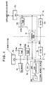
- Fig. 1 is a block diagram illustrating a system according to the present invention.
- Numeral 11 denotes the main system of a computer configuration, the system including a main system processor (CPU) lla, a ROM llb storing an initializing program (for the main system) PLD M for diagnostic/loading processing, a RAM 11c for storing a system program SPR M for the main system as well as the results of processing, a keyboard lld, a graphic display unit (CRT) lle, an external memory device 11f equipped with a disk controller DKC, a floppy disk (FD) and the like, and a DI/DO circuit for input/output of digital data.
- CPU main system processor
- ROM llb storing an initializing program (for the main system) PLD M for diagnostic/loading processing
- RAM 11c for storing a system program SPR M for the main system as well as the results of processing
- keyboard lld keyboard lld
- CRT graphic display unit
- FD floppy disk
- DI/DO circuit DI/DO circuit for input/output of digital
- Numeral 12 denotes a supplementary CPU board added to the main system 11 as for the purpose of function expansion and including a processor (CPU) 12a of the supplementary CPU, a RAM 12b for storing the system program SPR S of the supplementary CPU as well as the results of processing, and a DI/DO circuit 12c. It should be noted that the supplementary CPU board 12 is not provided with a ROM.
- Numeral 13 denotes a common RAM connected to the main system 11 and to the supplementary CPU board 12 by bus lines 14, 15 and arranged so as to be accessible by each of the CPU's.
- the common RAM 13 is composed of a RAM, a bus arbiter for performing traffic control in response to a read/write request from each CPU, etc.
- the common RAM 13 When seen from the CPU 12a of the supplementary CPU board 12, the common RAM 13 is so disposed that its leading address is the transition address. That is, though the address space of the supplementary CPU 12 is constituted by an address space AS 1 of the common RAM 13 and an address space AS 2 of the RAM 12b, as shown in Fig. 2, the CPU 12a reads commands and starts processing from the beginning of the common RAM 13 in response to execute-start enable (generation of the wake-up signal WKS).
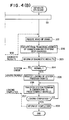
- Fig. 4 is a flowchart of system program loading processing, in which (A) is a flowchart of main CPU loading processing and (B) a flowchart of supplementary CPU loading processing.
- the CPU lla on the side of the main system 11 performs diagnostic processing (step 102) based on the diagnostic/loading processing program (initializing program) PLD M stored in the ROM 11b.
- the CPU 12a of the supplementary CPU does not start execution of processing until the wake-up signal WKS is generated.
- the CPU 11a stores the initializing program for the supplementary CPU 12a in the common RAM 13 in order starting from the leading address of the RAM (step 105), then sends the wake-up signal-WKS to the supplementary CPU 12 from the DI/DO circuit 11g (step 106), and thereafter assumes a standby state (step 107) until informed of the results of self-diagnosis from the supplementary CPU board 12.
- the supplementary CPU 12a assumes, by way of hardware, an execute-enable status (step 201), reads and executes the initializing program PLD S , one command at a time, from the transition address of the common RAM 13, performs diagnostic processing (step 202), and informs the main system 11 of the results via the common RAM 13 (step 203).
- the main system 11 and the supplementary CPU 12 each check to see whether the diagnostic results are normal (steps 1.08, 204). A system error occurs if an abnormality is found.
- the main system 11 assumes the standby state (step 109) until there is a loading request from the supplementary CPU 12a. Meanwhile, the supplementary CPU 12a requests the main system 11 to load its own system program SPR s via the common RAM 13 (step 205).
- the CPU lla of the main system reads the system program SPR s for the supplementary CPU out of the floppy disk FD of the external memory device llf and stores the system program in the common RAM 13 (step 110), then assumes the standby state (step 111) until informed by the supplementary CPU 12a that loading is completed, and terminates processing when informed of completion of loading.
- the supplementary CPU 12a transfers the system program to the RAM 12b (steps 206, 207), informs the main system 11 of the completion of loading (step 208) in response to completion of the transfer, and terminates processing.
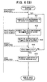
- Fig. 6 is a flowchart illustrating processing for saving a system program in accordance with the invention, in which (A) is a flowchart of main CPU saving processing and (B) a flowchart of supplementary CPU saving processing.
- the CPU lla on the main system side informs the supplementary CPU 12a, via the common RAM 13, of the fact that a save has been requested, and then awaits a save request from the supplementary CPU 12a (steps 301, 302).
- the CPU 12a When the supplementary CPU 12a is informed by the main system 11 of the fact a save has been requested, the CPU 12a is placed under the control of the saving program, stores part of the system program SPR s , which is the object of the save, in the common RAM 13 from the RAM 12c based on the saving program (step 401), requests the main system 11 to save the system program, which in the common RAM 13, in the external memory device 11f (step 402), and waits to be informed of output completion from the CPU lla (step 403).
- the main CPU lla When a command for save request is received from the supplementary CPU 12a, the main CPU lla outputs the part of the system program SPR s in the common RAM 13 to the external memory device 11f as simple data, informs the supplementary CPU 12a, via the common RAM 13, of the fact that output is completed (steps 303, 304), and thereafter waits to be informed of save completion or for a save request by the supplementary CPU 11a (steps 305, 306).
- the supplementary CPU 12a determines whether processing for saving the system program SPR s has been completed (step 404). If save processing has not been completed, the CPU 12a repeats processing from step 401 onward.
- the supplementary CPU 12a informs the main system 11, via the common RAM 13, of the fact that saving of the system program has been completed, and terminates saving processing (step 405).
- the CPU lla of the main system renders a "YES" decision at step 305 in response to being informed of the completion of the saving operation. Therefore, in accordance with the saving program contained in the system program SPR M stored in the RAM llc, the CPU 11a subsequently saves its own system program SPRM in the external memory device and ends processing (step 307).
- loading and saving of the system program for the supplementary CPU can be accomplished without providing the supplementary CPU board with a ROM.
- the main system is requested to output the system program to the external memory device.
- the entire system program on the side of the supplementary CPU is saved.
- the main system need not know the memory configuration on the side of the supplementary CPU and the configuration of the system files, maintenance can be performed with ease.
Landscapes
- Engineering & Computer Science (AREA)
- Theoretical Computer Science (AREA)
- Quality & Reliability (AREA)
- Physics & Mathematics (AREA)
- General Engineering & Computer Science (AREA)
- General Physics & Mathematics (AREA)
- Multi Processors (AREA)
- Stored Programmes (AREA)
Abstract
En réponse à une requête de sauvegarde d'un programme-système, le programme de sauvegarde du côté d'une unité centrale supplémentaire (12) transfère une partie de son propre programme-système (SPRS) depuis une mémoire vive (12b) vers une mémoire vive partagée (13) et demande ensuite à un système principal (11) d'envoyer le programme-système à une mémoire externe (11f). A la réception de cette demande, l'unité centrale (11a) du côté du système principal envoie le programme-système contenu par la mémoire vive partagée (13) sous forme de données simple à la mémoire (11f). Le traitement est ensuite répété et le programme-système (SPRS) du côté de l'unité centrale supplémentaire est sauvegardé dans la mémoire externe (11f).
Applications Claiming Priority (2)
| Application Number | Priority Date | Filing Date | Title |
|---|---|---|---|
| JP7153688A JPH01244562A (ja) | 1988-03-25 | 1988-03-25 | システムプログラムのセーブ方法 |
| JP71536/88 | 1988-03-25 |
Publications (2)
| Publication Number | Publication Date |
|---|---|
| EP0362403A1 true EP0362403A1 (fr) | 1990-04-11 |
| EP0362403A4 EP0362403A4 (en) | 1993-07-21 |
Family
ID=13463560
Family Applications (1)
| Application Number | Title | Priority Date | Filing Date |
|---|---|---|---|
| EP19890903257 Withdrawn EP0362403A4 (en) | 1988-03-25 | 1989-03-03 | Method of saving a system program |
Country Status (3)
| Country | Link |
|---|---|
| EP (1) | EP0362403A4 (fr) |
| JP (1) | JPH01244562A (fr) |
| WO (1) | WO1989009445A1 (fr) |
Family Cites Families (2)
| Publication number | Priority date | Publication date | Assignee | Title |
|---|---|---|---|---|
| JPS60254362A (ja) * | 1984-05-31 | 1985-12-16 | Fujitsu Ltd | デ−タ処理装置における状態情報の退避方法 |
| JPS61134859A (ja) * | 1984-12-04 | 1986-06-21 | Fujitsu Ltd | メモリのバツクアツプ制御方式 |
-
1988
- 1988-03-25 JP JP7153688A patent/JPH01244562A/ja active Pending
-
1989
- 1989-03-03 EP EP19890903257 patent/EP0362403A4/en not_active Withdrawn
- 1989-03-03 WO PCT/JP1989/000228 patent/WO1989009445A1/fr not_active Ceased
Non-Patent Citations (2)
| Title |
|---|
| No relevant documents disclosed * |
| See also references of WO8909445A1 * |
Also Published As
| Publication number | Publication date |
|---|---|
| JPH01244562A (ja) | 1989-09-28 |
| EP0362403A4 (en) | 1993-07-21 |
| WO1989009445A1 (fr) | 1989-10-05 |
Similar Documents
| Publication | Publication Date | Title |
|---|---|---|
| EP0106213B1 (fr) | Système décentralisé de traitement d'information et procédé d'introduction initiale du programme y relatif | |
| KR100215944B1 (ko) | 소비전력의 관리장치 및 방법 | |
| JP2829091B2 (ja) | データ処理システム | |
| US5283872A (en) | SCSI device having transfer parameter storage memory blocks which correspond to each apparatus | |
| EP0458304A1 (fr) | Appareil de commande de transfert pour l'accès direct en mémoire | |
| JP2002132701A (ja) | メモリ制御装置 | |
| US8150670B2 (en) | Simulator and simulation method | |
| JPH0746308B2 (ja) | 表示制御装置およびマイクロコンピュータ・システム | |
| JPS6022779B2 (ja) | 多重処理系のプログラム・ロ−デイング方法 | |
| US4652994A (en) | System for transmitting data to auxiliary memory device | |
| JP3079956B2 (ja) | プリンタ | |
| EP0766171A1 (fr) | Système de traitement d'information avec initialisation efficace après sa mise sous tension | |
| JPH0642227B2 (ja) | デ−タ転送装置 | |
| KR20000005448U (ko) | 프로세서 이중화 시스템 | |
| JP2980163B2 (ja) | データ転送方式 | |
| JPH08106432A (ja) | Dma制御回路 | |
| JPS63231545A (ja) | フアイル転送システム | |
| JPH03111961A (ja) | マルチcpuのプログラムロード方式 | |
| KR0171759B1 (ko) | 멀티프로세서 컴퓨터 시스템의 시스템제어 및 입출력처리기 | |
| JPS6012668B2 (ja) | ダイレクトメモリアクセス装置のインタ−フエイス回路 | |
| JP2002091520A (ja) | プログラマブルコントローラ及びメモリモジュール | |
| JPS6214869B2 (fr) | ||
| JPH09198302A (ja) | 主記憶制御回路及び主記憶装置 | |
| JPH0520253A (ja) | データ処理装置 | |
| JPH04120648A (ja) | 共通バス接続装置 |
Legal Events
| Date | Code | Title | Description |
|---|---|---|---|
| PUAI | Public reference made under article 153(3) epc to a published international application that has entered the european phase |
Free format text: ORIGINAL CODE: 0009012 |
|
| 17P | Request for examination filed |
Effective date: 19891124 |
|
| AK | Designated contracting states |
Kind code of ref document: A1 Designated state(s): DE FR GB IT |
|
| 16A | New documents despatched to applicant after publication of the search report | ||
| A4 | Supplementary search report drawn up and despatched |
Effective date: 19920810 |
|
| AK | Designated contracting states |
Kind code of ref document: A4 Designated state(s): DE FR GB IT |
|
| STAA | Information on the status of an ep patent application or granted ep patent |
Free format text: STATUS: THE APPLICATION IS DEEMED TO BE WITHDRAWN |
|
| 18D | Application deemed to be withdrawn |
Effective date: 19921001 |