EP0364806A2 - Flächenhafter Strahler - Google Patents
Flächenhafter Strahler Download PDFInfo
- Publication number
- EP0364806A2 EP0364806A2 EP89118295A EP89118295A EP0364806A2 EP 0364806 A2 EP0364806 A2 EP 0364806A2 EP 89118295 A EP89118295 A EP 89118295A EP 89118295 A EP89118295 A EP 89118295A EP 0364806 A2 EP0364806 A2 EP 0364806A2
- Authority
- EP
- European Patent Office
- Prior art keywords
- interconnect structure
- bodies
- semiconductor
- reflectors
- housing
- Prior art date
- Legal status (The legal status is an assumption and is not a legal conclusion. Google has not performed a legal analysis and makes no representation as to the accuracy of the status listed.)
- Granted
Links
Images

Classifications
-
- H—ELECTRICITY
- H10—SEMICONDUCTOR DEVICES; ELECTRIC SOLID-STATE DEVICES NOT OTHERWISE PROVIDED FOR
- H10W—GENERIC PACKAGES, INTERCONNECTIONS, CONNECTORS OR OTHER CONSTRUCTIONAL DETAILS OF DEVICES COVERED BY CLASS H10
- H10W90/00—Package configurations
-
- F—MECHANICAL ENGINEERING; LIGHTING; HEATING; WEAPONS; BLASTING
- F21—LIGHTING
- F21S—NON-PORTABLE LIGHTING DEVICES; SYSTEMS THEREOF; VEHICLE LIGHTING DEVICES SPECIALLY ADAPTED FOR VEHICLE EXTERIORS
- F21S43/00—Signalling devices specially adapted for vehicle exteriors, e.g. brake lamps, direction indicator lights or reversing lights
- F21S43/10—Signalling devices specially adapted for vehicle exteriors, e.g. brake lamps, direction indicator lights or reversing lights characterised by the light source
- F21S43/13—Signalling devices specially adapted for vehicle exteriors, e.g. brake lamps, direction indicator lights or reversing lights characterised by the light source characterised by the type of light source
- F21S43/14—Light emitting diodes [LED]
-
- H—ELECTRICITY
- H10—SEMICONDUCTOR DEVICES; ELECTRIC SOLID-STATE DEVICES NOT OTHERWISE PROVIDED FOR
- H10H—INORGANIC LIGHT-EMITTING SEMICONDUCTOR DEVICES HAVING POTENTIAL BARRIERS
- H10H20/00—Individual inorganic light-emitting semiconductor devices having potential barriers, e.g. light-emitting diodes [LED]
- H10H20/80—Constructional details
- H10H20/85—Packages
- H10H20/852—Encapsulations
- H10H20/853—Encapsulations characterised by their shape
-
- H—ELECTRICITY
- H10—SEMICONDUCTOR DEVICES; ELECTRIC SOLID-STATE DEVICES NOT OTHERWISE PROVIDED FOR
- H10H—INORGANIC LIGHT-EMITTING SEMICONDUCTOR DEVICES HAVING POTENTIAL BARRIERS
- H10H20/00—Individual inorganic light-emitting semiconductor devices having potential barriers, e.g. light-emitting diodes [LED]
- H10H20/80—Constructional details
- H10H20/85—Packages
- H10H20/855—Optical field-shaping means, e.g. lenses
- H10H20/856—Reflecting means
-
- H—ELECTRICITY
- H10—SEMICONDUCTOR DEVICES; ELECTRIC SOLID-STATE DEVICES NOT OTHERWISE PROVIDED FOR
- H10H—INORGANIC LIGHT-EMITTING SEMICONDUCTOR DEVICES HAVING POTENTIAL BARRIERS
- H10H20/00—Individual inorganic light-emitting semiconductor devices having potential barriers, e.g. light-emitting diodes [LED]
- H10H20/80—Constructional details
- H10H20/85—Packages
- H10H20/857—Interconnections, e.g. lead-frames, bond wires or solder balls
-
- F—MECHANICAL ENGINEERING; LIGHTING; HEATING; WEAPONS; BLASTING
- F21—LIGHTING
- F21S—NON-PORTABLE LIGHTING DEVICES; SYSTEMS THEREOF; VEHICLE LIGHTING DEVICES SPECIALLY ADAPTED FOR VEHICLE EXTERIORS
- F21S43/00—Signalling devices specially adapted for vehicle exteriors, e.g. brake lamps, direction indicator lights or reversing lights
- F21S43/20—Signalling devices specially adapted for vehicle exteriors, e.g. brake lamps, direction indicator lights or reversing lights characterised by refractors, transparent cover plates, light guides or filters
- F21S43/281—Materials thereof; Structures thereof; Properties thereof; Coatings thereof
- F21S43/28135—Structures encapsulating the light source
-
- F—MECHANICAL ENGINEERING; LIGHTING; HEATING; WEAPONS; BLASTING
- F21—LIGHTING
- F21Y—INDEXING SCHEME ASSOCIATED WITH SUBCLASSES F21K, F21L, F21S and F21V, RELATING TO THE FORM OR THE KIND OF THE LIGHT SOURCES OR OF THE COLOUR OF THE LIGHT EMITTED
- F21Y2105/00—Planar light sources
- F21Y2105/10—Planar light sources comprising a two-dimensional [2D] array of point-like light-generating elements
-
- F—MECHANICAL ENGINEERING; LIGHTING; HEATING; WEAPONS; BLASTING
- F21—LIGHTING
- F21Y—INDEXING SCHEME ASSOCIATED WITH SUBCLASSES F21K, F21L, F21S and F21V, RELATING TO THE FORM OR THE KIND OF THE LIGHT SOURCES OR OF THE COLOUR OF THE LIGHT EMITTED
- F21Y2107/00—Light sources with three-dimensionally disposed light-generating elements
- F21Y2107/70—Light sources with three-dimensionally disposed light-generating elements on flexible or deformable supports or substrates, e.g. for changing the light source into a desired form
-
- F—MECHANICAL ENGINEERING; LIGHTING; HEATING; WEAPONS; BLASTING
- F21—LIGHTING
- F21Y—INDEXING SCHEME ASSOCIATED WITH SUBCLASSES F21K, F21L, F21S and F21V, RELATING TO THE FORM OR THE KIND OF THE LIGHT SOURCES OR OF THE COLOUR OF THE LIGHT EMITTED
- F21Y2115/00—Light-generating elements of semiconductor light sources
- F21Y2115/10—Light-emitting diodes [LED]
-
- Y—GENERAL TAGGING OF NEW TECHNOLOGICAL DEVELOPMENTS; GENERAL TAGGING OF CROSS-SECTIONAL TECHNOLOGIES SPANNING OVER SEVERAL SECTIONS OF THE IPC; TECHNICAL SUBJECTS COVERED BY FORMER USPC CROSS-REFERENCE ART COLLECTIONS [XRACs] AND DIGESTS
- Y10—TECHNICAL SUBJECTS COVERED BY FORMER USPC
- Y10S—TECHNICAL SUBJECTS COVERED BY FORMER USPC CROSS-REFERENCE ART COLLECTIONS [XRACs] AND DIGESTS
- Y10S362/00—Illumination
- Y10S362/80—Light emitting diode
Definitions
- the invention relates to a planar radiator according to the preamble of claim 1.
- Incandescent lamps usually together with a reflector, are generally used in planar spotlights, for example automotive lights.
- incandescent lamps have a limited lifespan and, due to the dimensions of the bulb, they also have a relatively large overall depth.
- luminescent diodes have the advantage that they have a longer lifespan and therefore work more reliably, that they have better electro-optical efficiency and therefore lower energy requirements, and that their flat structure allows smaller installation depths. Luminescent diodes are therefore preferred wherever replacing individual lamps is cumbersome and expensive and where high demands are placed on the reliability, safety and long-term stability of the spotlight.
- the spotlights have a curved shape.
- the glass plate on which the luminescent semiconductor bodies are mounted cannot be brought into the desired curved shape, for example by bending. You must therefore have a curved shape during manufacture; mounting the semiconductor body on a curved surface is associated with great difficulties.
- the invention has for its object to avoid these disadvantages and to provide a radiator in which a simple assembly of the semiconductor body is possible and which can nevertheless assume a required curved shape.
- the semiconductor bodies are arranged in a number corresponding to the respective requirements, for example the required light intensity or curvature of the emitter, on the interconnect structure, preferably in a uniform distribution. With a required high radiation power, the semiconductor bodies border at most so closely to one another that the mobility of the interconnect structure is not restricted.
- the method of manufacturing the interconnect structure and the assembly of the luminescence semiconductor bodies on the planar interconnect structure is explained with reference to FIG. 1.
- Metal strips are punched out of a sheet metal or a metal plate, whereby a certain shape ensures that stretchable interconnect pieces 2b and auxiliary connections 12 are present.
- the metal strips 2a, 2b are specially coated, for example with a nickel adhesive layer and an overlying silver layer, and serve as interconnects for contacting and interconnecting the semiconductor bodies 1.
- the auxiliary connections 12 are used for mechanically stabilizing the interconnect structure 2.
- the connectors 12a from the interconnect structure 2 to the auxiliary Connections 12 are preferably made outside the area of the semiconductor bodies 3, 5, ie in the movable part 2b of the interconnect structure, in order to ensure optimum radiation utilization.
- the semiconductor bodies 1, which have an extent of 250 ⁇ m ⁇ 250 ⁇ m, for example, are glued or soldered onto the part 2a of the planar interconnect structure, preferably by automatic assembly, and are bonded to the next strip position, i.e. by means of bonding wires 7. the next track section.
- those points on the interconnect structure at which the semiconductor bodies 1 are to be attached are dripped with a conductive adhesive.
- the semiconductor bodies are then inserted into these drops and the adhesive is cured at a temperature of, for example, 150 ° C.
- the interconnect structure 2 with the semiconductor bodies 1 fastened and contacted thereon is now placed on a preferably parabolic mold in such a way that the semiconductor body 1 is in the focal point of the parabola and the movable parts 2b of the interconnect structure are located between the cutouts in the mold.
- the mold is preferably made of a plastic material and can be produced in the desired shape by means of plastic injection molding technology.
- the casting mold is cast with a plastic casting compound, for example silicone resin, epoxy resin, polyimide or polyphenylene sulfide.
- Each semiconductor body 1 is thus located in the focal point of the parabolic plastic housing body 3.
- the outer surface of the plastic body 3 can be coated using a highly reflective material, for example aluminum or silver, to form the reflectors 6a. It is important to ensure that the electrical leads 2a are not short-circuited. Due to the parabolic shape of the reflectors 6a, the entire reflected radiation 9 is bundled in parallel, so that the greatest possible light intensity is obtained.
- the auxiliary connections 12 for stabilizing the interconnect structure are no longer required and are removed again by cutting free along the dash-dotted lines in FIG. 1. The entire radiator is then pressed against a base in the desired, for example curved, shape.
- the movable interconnect pieces 2b which are located between the housing bodies 3, ensure that the radiator can take on any shape.
- the underlay can also serve as a stabilizing rear wall; the spotlight is then fixed on this base, for example by gluing. If the casting mold is required, for example, for reasons of stability or as protection for the reflecting surfaces, it is not removed after the casting compound has hardened; however, it must already have the desired shape of the emitter.
- the inside of the casting mold is then designed to be highly reflective, for which purpose it can be coated, for example, with a highly reflective material before the casting compound is introduced.
- the contact surface 8 on the back of the semiconductor body is designed to be highly reflective, so that the one emitted in the direction of the interconnect structure Radiation is largely reflected and contributes to the radiation 9 emitted directly in the direction of the reflector and reflected there and thus to the total emission, which results in a high collection efficiency.
- the reflectors 6b are designed as a hollow shape by virtue of a shaped body 4.
- the assembly and contacting of the semiconductor body 1 on the interconnect structure 2 is carried out in exactly the same way as was described with reference to FIG. 1.
- the semiconductor bodies are dripped with a synthetic resin which has a refractive index of, for example, 1.5, so that the semiconductor bodies 1 are embedded in a housing body 5.
- the interconnect structure 2 with the semiconductor bodies 1 is placed on the molded body 4, which must already have the desired shape of the radiator and can serve, for example, as the rear wall of the housing.
- the interconnect structure 2 is connected to the molded body 4 without potting, for example by gluing at certain points on the interconnects.
- the inside of the molded body is highly reflective and can be coated with a highly reflective material, for example, before joining the interconnect structure.
- predominantly only the radiation 9 reflected by means of the reflector 6b is coupled out.
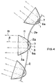
- a radiator according to FIG. 2 is first formed as a full mold and then further plastic bodies 3 a, which can be produced by means of separate casting molds or injection molds, for example attached to the top of the interconnect structure by an optical adhesive.
- additional plastic bodies 3a have the shape of a parabolic stump and are glued to the top of the interconnect structure in such a way that the housing bodies 3, 3a below and above the interconnect structure 2 together produce a parabolic profile.
- the outer surfaces of the plastic body 3a are coated to form reflectors 11 by means of a highly reflective material.
- both a large part of the radiation 10 emitted towards the interconnect structure is bundled by the reflectors 11 and the radiation 9 reflected on the reflectors 6a, so that the light intensity and the light utilization rate increase.
- the plastic bodies 3a of the reflectors 11 above the interconnect structure preferably consist of the same material as the plastic bodies 3 of the reflectors 6a below the interconnect structure.
- the contacting and wiring of the semiconductor body 1 according to FIG. 1 depends on the specification of the radiator.
- the semiconductor body 1 can be attached to the entire available area and connected in series to increase the operating voltage and / or connected in parallel to achieve the necessary light intensity.
- This interconnection can be varied as desired in accordance with the given layout of the interconnect structure 2.
- the semiconductor bodies 1 are preferably arranged on the interconnect structure 2 in such a way that a maximum light intensity is achieved for certain requirements.
- the housing bodies 3, 5 can adjoin one another so closely that, on the one hand, the space available on the interconnect structure is optimally utilized without, on the other hand, the mobility of the interconnect structure being restricted too much.
- the shape of the emitter, the number of luminescent diodes used, their interconnection and the wavelength of the emitted radiation can be specified exactly according to the specific requirements.
- the spectral range of the emitted radiation can also easily be in the infrared range, e.g. B. can be moved by equipping with GaAs diodes.
- the luminescent diodes used typically have a forward voltage of 2 V and a permissible current of 50 mA, so that for example for an operating voltage of 12 V approximately 5-6 diodes have to be connected in series.
- the luminous flux of a single luminescent diode is typically 1-4 lm, the luminous intensity is approximately 1-3 cd; for a motor vehicle brake light, for example, the light intensity must be between 40 cd and 100 cd.
- GaAlAs heterostructure diodes can be used, the maximum emission of which is 660 nm.
- the radiator according to the invention can be used in many ways; For example, it is conceivable to use it as a vehicle light, signal light or position light.
Landscapes
- Engineering & Computer Science (AREA)
- Physics & Mathematics (AREA)
- Microelectronics & Electronic Packaging (AREA)
- Optics & Photonics (AREA)
- General Engineering & Computer Science (AREA)
- Non-Portable Lighting Devices Or Systems Thereof (AREA)
- Planar Illumination Modules (AREA)
- Led Device Packages (AREA)
- Arrangement Of Elements, Cooling, Sealing, Or The Like Of Lighting Devices (AREA)
Abstract
Description
- Die Erfindung betrifft einen flächenhaften Strahler nach dem Oberbegriff des Anspruchs 1.
In flächenhaften Strahlern, beispielsweise Kfz-Leuchten, werden in der Regel Glühlampen, meist zusammen mit einem Reflektor, eingesetzt. Glühlampen besitzen aber nur eine begrenzte Lebensdauer, zudem hat man, bedingt durch die Abmessungen der Birne, eine relativ große Bautiefe. - Lumineszenzdioden haben demgegenüber den Vorteil, daß sie eine größere Lebensdauer besitzen und daher zuverlässiger arbeiten, daß sie einen besseren elektro-optischen Wirkungsgrad und deshalb geringeren Energiebedarf aufweisen und daß wegen ihrer flachen Struktur kleinere Bautiefen möglich sind. Lumineszenzdioden werden daher bevorzugt dort eingesetzt, wo ein Austausch einzelner Lampen umständlich und teuer ist und wo hohe Anforderungen an die Zuverlässigkeit, Sicherheit und Langzeitstabilität des Strahlers gestellt werden.
- Um einen Strahler mit hohem Wirkungsgrad und in flacher Bauweise herzustellen, wurde bereits vorgeschlagen, Lumineszenz-Halbleiterkörper, die jeweils von einem Gehäusekörper umgeben sind, in einer flächenhaften Verteilung auf einer ebenen Glasplatte zu montieren.
- In vielen Anwendungsfällen, beispielsweise im Kfz-Bereich, besitzen die Strahler eine gekrümmte Form.
- Die Glasplatte, auf der die Lumineszenz-Halbleiterkörper montiert werden, kann jedoch nicht in die gewünschte gekrümmte Form, beispielsweise durch Verbiegen, gebracht werden. Sie muß daher bereits bei der Herstellung eine gekrümmte Form besitzen; eine Montage der Halbleiterkörper auf einer gekrümmten Oberfläche ist jedoch mit großen Schwierigkeiten verbunden.
- Der Erfindung liegt die Aufgabe zugrunde, diese Nachteile zu vermeiden und einen Strahler anzugeben, bei dem eine einfache Montage der Halbleiterkörper möglich ist und der dennoch eine geforderte gekrümmte Form annehmen kann.
Dies wird erfindungsgemäß dadurch erreicht, daß die Leitbahnstruktur zwischen den einzelnen Gehäusekörpern derart beweglich ausgebildet ist, daß der Strahler in eine beliebig gekrümmte Form gebracht werden kann. - Weitere vorteilhafte Ausgestaltungen der Erfindung ergeben sich aus den Unteransprüchen.
- Die Halbleiterkörper sind in einer den jeweiligen Bedürfnissen, z.B. geforderte Lichtstärke oder Krümmung des Strahlers, entsprechenden Anzahl auf der Leitbahnstruktur, vorzugsweise in einer gleichmäßigen Verteilung, angeordnet. Bei einer geforderten hohen Strahlungsleistung grenzen die Halbleiterkörper höchstens so dicht aneinander, daß die Beweglichkeit der Leitbahnstruktur nicht eingeschränkt wird.
- Der Herstellungsprozeß des erfindungsgemäßen Strahlers und seine Ausführungsformen sollen nun anhand der Figuren 1 - 4 beschrieben werden. Es zeigen:
- Figur 1 Eine Aufsicht auf die Leitbahnstruktur mit den Halbleiterkörpern.
- Figur 2 Eine Schnittdarstellung des flächenhaften Strahlers, bei dem die Reflektoren als Vollform ausgebildet sind.
- Figur 3 Eine Schnittdarstellung des flächenhaften Strahlers, bei dem die Reflektoren als Hohlform ausgebildet sind.
- Figur 4 Eine Schnittdarstellung des flächenhaften Strahlers, bei dem die als Vollform ausgebildeten Reflektoren sowohl unterhalb als auch oberhalb der Leitbahnstruktur angeordnet sind.
- Das Herstellungsverfahren der Leitbahnstruktur und die Montage der Lumineszenz-Halbleiterkörper auf der planaren Leitbahnstruktur wird anhand der Figur 1 erläutert. Aus einem Blech oder einer Metallplatte werden Metallstreifen ausgestanzt, wobei durch eine bestimmte Formgebung erreicht wird, daß dehnbare Leitbahnstücke 2b sowie Hilfsverbindungen 12 vorhanden sind. Die Metallstreifen 2a, 2b werden speziell beschichtet, beispielsweise mit einer Nickel-Haftschicht und einer darüber liegenden Silberschicht und dienen als Leitbahnen zur Kontaktierung und Zusammenschaltung der Halbleiterkörper 1. Die Hilfsverbindungen 12 werden zur mechanischen Stabilisierung der Leitbahnstruktur 2 verwendet. Die Verbindungsstücke 12a von der Leitbahnstruktur 2 zu den Hilfs verbindungen 12 werden vorzugsweise außerhalb des Bereichs der Halbleiterkörper 3, 5, d.h. im beweglichen Teil 2b der Leitbahnstruktur angebracht, um eine optimale Strahlungsausnutzung zu gewährleisten.
- Die Halbleiterkörper 1, die beispielsweise eine Ausdehnung von 250 µm x 250 µm besitzen, werden, vorzugsweise durch automatische Bestückung, auf den Teil 2a der planaren Leitbahnstruktur aufgeklebt oder aufgelötet und durch Bonddrähte 7 mit der nächsten Streifenposition, d.h. dem nächsten Leitbahnstück, verbunden. Beispielsweise werden diejenigen Stellen auf der Leitbahnstruktur, an denen die Halbleiterkörper 1 angebracht werden sollen, mit einem leitfähigen Kleber betropft. In diese Tropfen werden dann die Halbleiterkörper eingesetzt und der Kleber bei einer Temperatur von beispielsweise 150 °C ausgehärtet.
- Anhand der Figur 2 wird ein Ausführungsbeispiel beschrieben, bei dem die Reflektoren als Vollform ausgebildet sind.
Die Leitbahnstruktur 2 mit den darauf befestigten und kontaktierten Halbleiterkörpern 1 wird nun derart auf eine vorzugsweise parabelförmige Gießform gelegt, daß sich die Halbleiterkörper 1 im Brennpunkt der Parabel und die beweglichen Teile 2b der Leitbahnstruktur zwischen den Aussparungen der Gießform befinden. Die Gießform besteht vorzugsweise aus einem Kunststoff-Material und kann mittels der Kunststoff-Spritzgußtechnik in der gewünschten Form hergestellt werden. Zur Herstellung der Reflektoren 6a wird die Gießform mit einer Kunststoff-Vergußmasse, beispielsweise Siliconharz, Epoxidharz, Polyimid oder Polyphenylensulfid ausgegossen. Jeder Halbleiterkörper 1 befindet sich somit im Brennpunkt des parabolischen Kunststoff-Gehäusekörpers 3. Nach dem Härten der Vergußmasse bei beispielsweise 150 °C und der Entformung durch die Entfernung der Gießform kann die Außenfläche des Kunststoffkörpers 3 zur Bildung der Reflektoren 6a mittels eines hochreflektierenden Materials, beispielsweise Aluminium oder Silber, beschichtet werden. Dabei ist darauf zu achten, daß die elektrischen Zuleitungen 2a nicht kurzgeschlossen werden.
Durch die parabolische Form der Reflektoren 6a wird die gesamte reflektierte Strahlung 9 parallel gebündelt, so daß man die größtmögliche Lichtstärke erhält.
Die Hilfsverbindungen 12 zur Stabilisierung der Leitbahnstruktur werden nun nicht mehr benötigt und durch Freischneiden entlang den strichpunktierten Linien in Figur 1 wieder entfernt. Anschließend wird der gesamte Strahler gegen eine Unterlage in die gewünschte, beispielsweise gekrümmte Form gedrückt. Durch die beweglichen Leitbahnstücke 2b, die sich zwischen den Gehäusekörpern 3 befinden, ist gewährleistet, daß der Strahler eine beliebige Form annehmen kann.
Die Unterlage kann dabei gleichzeitig als stabilisierende Rückwand dienen; der Strahler wird dann auf dieser Unterlage, beispielsweise durch Verkleben, fixiert. Falls die Gießform z.B. aus Stabilitätsgründen oder als Schutz für die reflektierenden Flächen benötigt wird, wird sie nach dem Aushärten der Vergußmasse nicht entfernt; sie muß dann allerdings bereits die gewünschte Form des Strahlers besitzen. Die Innenseite der Gießform ist dann hochreflektierend ausgebildet, wozu sie vor dem Einbringen der Vergußmasse beispielsweise mit einem hochreflektierenden Material beschichtet werden kann.
Die Kontaktfläche 8 auf der Rückseite des Halbleiterkörpers wird möglichst hochreflektierend ausgebildet, so daß die in Richtung Leitbahnstruktur emittierte Strahlung größtenteils reflektiert wird und zu der direkt in Richtung Reflektor emittierten und dort reflektierten Strahlung 9 und somit zur Gesamtemission beiträgt, woraus sich ein hoher Sammelwirkungsgrad ergibt. - In einer anderen Ausführungsform gemäß Figur 3, sind die Reflektoren 6b vermöge eines Formkörpers 4 als Hohlform ausgebildet.
Die Montage und Kontaktierung der Halbleiterkörper 1 auf der Leitbahnstruktur 2 wird genauso durchgeführt, wie dies anhand der Figur 1 beschrieben wurde. Um die Strahlungsauskopplung aus dem Lumineszenz-Halbleiterkörper 1 zu verbessern, werden die Halbleiterkörper mit einem Kunstharz, der einen Brechungsindex von beispielsweise 1,5 besitzt, betropft, so daß die Halbleiterkörper 1 in einem Gehäusekörper 5 eingebettet sind. Die Leitbahnstruktur 2 mit den Halbleiterkörpern 1 wird nach dem Entfernen der Hilfsverbindungen 12 auf den Formkörper 4 gelegt, der bereits die gewünschte Form des Strahlers besitzen muß, und beispielsweise als Gehäuserückwand dienen kann. Die Leitbahnstruktur 2 wird ohne Vergießen mit dem Formkörper 4 verbunden, beispielsweise durch Kleben an bestimmten Stellen der Leitbahnen. Die Innenseite des Formkörpers ist hochreflektierend und kann beispielsweise vor dem Zusammenschluß mit der Leitbahnstruktur mit einem hochreflektierenden Material beschichtet werden. Auch hier wird überwiegend nur die mittels des Reflektors 6b reflektierte Strahlung 9 ausgekoppelt. - Bei einer weiteren, in Figur 4 dargestellten Ausführungsform, wird zunächst ein Strahler gemäß Figur 2 als Vollform ausgebildet und anschließend weitere Kunststoffkörper 3a, die mittels separater Gießformen oder Spritzformen hergestellt werden können, beispielsweise vermöge eines optischen Klebers auf der Oberseite der Leitbahnstruktur angebracht. Diese zusätzlichen Kunststoffkörper 3a besitzen die Form eines Parabelstumpfs und werden so auf die Oberseite der Leitbahnstruktur geklebt, daß die Gehäusekörper 3, 3a unterhalb und oberhalb der Leitbahnstruktur 2 zusammen ein parabolisches Profil ergeben. Die Außenflächen der Kunststoffkörper 3a werden zur Bildung von Reflektoren 11 mittels eines hochreflektierenden Materials beschichtet. Bei dieser Ausführungsform wird sowohl ein Großteil der zur Leitbahnstruktur hin emittierten Strahlung 10 durch die Reflektoren 11 als auch die an den Reflektoren 6a reflektierte Strahlung 9 gebündelt, so daß die Lichtstärke und der Lichtnutzungsgrad ansteigt.
Die Kunststoffkörper 3a der Reflektoren 11 oberhalb der Leitbahnstruktur bestehen vorzugsweise aus dem gleichen Material wie die Kunststoffkörper 3 der Reflektoren 6a unterhalb der Leitbahnstruktur. - Die Kontaktierung und Verdrahtung der Halbleiterkörper 1 gemäß der Figur 1 richtet sich nach der Spezifikation des Strahlers. Die Halbleiterkörper 1 können auf der gesamten zu Verfügung stehenden Fläche angebracht und zur Erhöhung der Betriebsspannung hintereinandergeschaltet und/oder zur Erzielung der notwendigen Lichtstärke parallelgeschaltet werden. Diese Zusammenschaltung ist dabei gemäß des vorgegebenen Layouts der Leitbahnstruktur 2 beliebig variierbar.
Vorzugsweise werden die Halbleiterkörper 1 derart auf der Leitbahnstruktur 2 angeordnet, daß für bestimmte Anforderungen eine maximale Lichtstärke erzielt wird. Dazu können beispielsweise die Gehäusekörper 3, 5 so dicht aneinandergrenzen, daß einerseits der auf der Leitbahnstruktur zur Verfügung stehende Platz optimal ausgenutzt wird ohne daß aber dabei andererseits die Beweglichkeit der Leitbahnstruktur zu sehr eingeschränkt wird. - Die Form des Strahlers, die Zahl der verwendeten Lumineszenzdioden, deren Verschaltung sowie die Wellenlänge der emittierten Strahlung kann dabei exakt nach den spezifischen Anforderungen vorgegeben werden, wobei der Spektralbereich der emittierten Strahlung ohne weiteres auch in den infraroten Bereich, z. B. durch Bestückung mit GaAs-Dioden, verschoben werden kann.
- Die verwendeten Lumineszenzdioden besitzen typischerweise eine Flußspannung von 2 V und eine zulässige Stromstärke von 50 mA, so daß beispielsweise für eine Betriebsspannung von 12 V ca. 5 - 6 Dioden hintereinander geschaltet werden müssen.
Der Lichtstrom einer Einzel-Lumineszenzdiode beträgt typischerweise 1 - 4 lm, die Lichtstärke ca. 1 - 3 cd; für eine Kfz-Bremsleuchte beispielsweise muß die Lichtstärke zwischen 40 cd und 100 cd liegen.
Um beispielsweise Rotlicht-emittierende Strahler zu erhalten, können GaAlAs-Heterostrukturdioden eingesetzt werden, deren maximale Emission bei 660 nm liegt. Der erfindungsgemäße Strahler ist vielfältig einsetzbar; denkbar ist beispielsweise die Verwendung als Kfz-Leuchte, Signalleuchte oder Begrenzungsleuchte.
Claims (15)
Applications Claiming Priority (2)
| Application Number | Priority Date | Filing Date | Title |
|---|---|---|---|
| DE3835942A DE3835942A1 (de) | 1988-10-21 | 1988-10-21 | Flaechenhafter strahler |
| DE3835942 | 1988-10-21 |
Publications (3)
| Publication Number | Publication Date |
|---|---|
| EP0364806A2 true EP0364806A2 (de) | 1990-04-25 |
| EP0364806A3 EP0364806A3 (de) | 1991-03-13 |
| EP0364806B1 EP0364806B1 (de) | 1993-01-20 |
Family
ID=6365653
Family Applications (1)
| Application Number | Title | Priority Date | Filing Date |
|---|---|---|---|
| EP89118295A Expired - Lifetime EP0364806B1 (de) | 1988-10-21 | 1989-10-03 | Flächenhafter Strahler |
Country Status (5)
| Country | Link |
|---|---|
| US (1) | US5084804A (de) |
| EP (1) | EP0364806B1 (de) |
| JP (1) | JP3037346B2 (de) |
| KR (1) | KR0138109B1 (de) |
| DE (2) | DE3835942A1 (de) |
Cited By (23)
| Publication number | Priority date | Publication date | Assignee | Title |
|---|---|---|---|---|
| EP0590336A1 (de) * | 1992-10-02 | 1994-04-06 | TEMIC TELEFUNKEN microelectronic GmbH | Optoelektronisches Bauelement mit engem Öffnungswinkel |
| EP0921568A3 (de) * | 1997-11-25 | 2000-04-12 | Matsushita Electric Works, Ltd. | Leuchte mit lichtemittierenden Dioden |
| DE10025563A1 (de) * | 2000-05-24 | 2001-12-06 | Osram Opto Semiconductors Gmbh | Modul für die Anordnung von elektrischen lichtemittierenden Elementen und Verfahren zur Herstellung eines derartigen Moduls |
| DE10129950A1 (de) * | 2001-06-21 | 2003-01-02 | Hella Kg Hueck & Co | Leuchte für Fahrzeuge und Verfahren zur Herstellung derselben |
| DE20204219U1 (de) * | 2002-03-16 | 2003-07-31 | Büchner, Thomas, 86465 Welden | Variable Beleuchtungseinrichtung |
| DE10232894A1 (de) * | 2002-07-19 | 2004-01-29 | Bayerische Motoren Werke Ag | Leuchte mit mindestens einer Leuchtdiode als Leuchtmittel |
| DE10234102A1 (de) * | 2002-07-26 | 2004-02-12 | Hella Kg Hueck & Co. | Leuchtdiodenanordnung |
| US6809475B2 (en) | 2000-06-15 | 2004-10-26 | Lednium Pty Limited | Led lamp with light-emitting junctions arranged in a three-dimensional array |
| EP1564481A1 (de) * | 2004-02-13 | 2005-08-17 | Valeo Vision | Beleuchtungsmodul für Kfz-Scheinwerfer, Reflektor für ein solches Modul, und Kfz-Scheinwerfer umfassend dieses Modul |
| DE19921684B4 (de) * | 1999-05-12 | 2006-01-19 | Vossloh-Schwabe Optoelectronic Gmbh & Co. Kg | Beleuchtungselement mit Halbleiterchips |
| US7320632B2 (en) | 2000-06-15 | 2008-01-22 | Lednium Pty Limited | Method of producing a lamp |
| WO2008114200A1 (en) * | 2007-03-22 | 2008-09-25 | Koninklijke Philips Electronics N.V. | Flexible light source |
| EP1244152A3 (de) * | 2001-01-26 | 2008-12-03 | Toyoda Gosei Co., Ltd. | Reflektierende lichtemittierende Diode, reflektierende optische Vorrichtung und Herstellungsverfahren |
| EP1652726A3 (de) * | 2004-10-29 | 2010-04-14 | Hitachi Ltd. | Vorrichtung zur Kontrolle der Lichtverteilung |
| US7704762B2 (en) | 2002-06-14 | 2010-04-27 | Lednium Technology Pty Limited | Lamp and method of producing a lamp |
| WO2011073018A1 (de) * | 2009-12-18 | 2011-06-23 | Osram Gesellschaft mit beschränkter Haftung | Led-beleuchtungsvorrichtung |
| WO2012000943A1 (de) * | 2010-06-28 | 2012-01-05 | Osram Opto Semiconductors Gmbh | Verfahren zur herstellung eines oberflächenmontierbaren halbleiterbauelements |
| WO2014207620A1 (en) * | 2013-06-28 | 2014-12-31 | Koninklijke Philips N.V. | Bonding led die to lead frame strips |
| WO2015176972A1 (en) * | 2014-05-20 | 2015-11-26 | Koninklijke Philips N.V. | Conformal coated lighting or lumination system |
| WO2015180978A1 (en) * | 2014-05-30 | 2015-12-03 | Koninklijke Philips N.V. | Leds mounted on curved lead frame |
| EP3203141A1 (de) * | 2016-02-08 | 2017-08-09 | Zumtobel Lighting GmbH | Leuchtenoptik, leuchtenoptiksystem sowie leuchte mit leuchtenoptik |
| WO2021224130A1 (de) * | 2020-05-04 | 2021-11-11 | Osram Opto Semiconductors Gmbh | Optoelektronisches bauelement und verfahren zum herstellen eines optoelektronischen bauelements |
| EP4660525A1 (de) * | 2020-08-11 | 2025-12-10 | Lg Innotek Co. Ltd | Llightvorrichtung und fahrzeug damit |
Families Citing this family (54)
| Publication number | Priority date | Publication date | Assignee | Title |
|---|---|---|---|---|
| JPH04106043U (ja) * | 1991-02-25 | 1992-09-11 | 日本板硝子株式会社 | 自動車用ストツプランプ |
| US5567036A (en) * | 1995-04-05 | 1996-10-22 | Grote Industries, Inc. | Clearance and side marker lamp |
| US5519596A (en) * | 1995-05-16 | 1996-05-21 | Hewlett-Packard Company | Moldable nesting frame for light emitting diode array |
| US5613751A (en) * | 1995-06-27 | 1997-03-25 | Lumitex, Inc. | Light emitting panel assemblies |
| US5871271A (en) * | 1995-11-30 | 1999-02-16 | Chien; Tseng Lu | LED illuminated protective headwear |
| DE19621148A1 (de) * | 1996-05-14 | 1997-12-04 | Magna Reflex Holding Gmbh | Leuchtelement |
| DE19627856A1 (de) * | 1996-07-11 | 1998-01-15 | Happich Fahrzeug & Ind Teile | Beleuchtungsleiste und Verfahren zur Herstellung |
| US5920643A (en) * | 1997-05-16 | 1999-07-06 | Northeast Robotics Llc | Flexible lighting element circuit and method of manufacturing the same |
| US5912777A (en) * | 1997-06-26 | 1999-06-15 | The United States Of America As Represented By The Administrator Of The National Aeronautics And Space Administration | High temperature solar reflector, its preparation and use |
| DE19727701A1 (de) * | 1997-06-30 | 1999-01-07 | Bosch Gmbh Robert | Lichtquellenanordnung |
| DE29817609U1 (de) * | 1998-09-02 | 2000-01-13 | Derksen, Gabriele, 45889 Gelsenkirchen | Leuchtmittel |
| DE19902750A1 (de) | 1999-01-25 | 2000-08-03 | Osram Opto Semiconductors Gmbh | Halbleiterbauelement zur Erzeugung von mischfarbiger elektromagnetischer Strahlung |
| DE19909399C1 (de) * | 1999-03-04 | 2001-01-04 | Osram Opto Semiconductors Gmbh | Flexibles LED-Mehrfachmodul, insb. für ein Leuchtengehäuse eines Kraftfahrzeuges |
| DE19938734A1 (de) * | 1999-08-16 | 2001-03-01 | Fer Fahrzeugelektrik Gmbh | Fahrzeugleuchte |
| KR100572442B1 (ko) * | 1999-11-30 | 2006-04-18 | 오므론 가부시키가이샤 | 광학 장치 |
| DE19959609A1 (de) * | 1999-12-10 | 2001-06-28 | Volkswagen Ag | Außenrückspiegel mit integriertem Fahrtrichtungsanzeiger |
| DE20002565U1 (de) * | 2000-02-14 | 2001-06-28 | Zumtobel Staff Ges.M.B.H., Dornbirn | Leuchtdiodenanordnung mit Reflektor |
| AU756072B2 (en) * | 2000-06-15 | 2003-01-02 | Lednium Technology Pty Limited | Led lamp |
| IT1320547B1 (it) * | 2000-07-21 | 2003-12-10 | Fiat Ricerche | Dispositivo di illuminazione, particolarmente proiettore o fanale diautoveicolo con distribuzione a matrice di sorgenti luminose |
| DE10063876B4 (de) | 2000-12-21 | 2009-02-26 | Continental Automotive Gmbh | Aus einer Vielzahl von Leuchtdioden bestehende Lichtquelle |
| JP4216603B2 (ja) * | 2001-03-02 | 2009-01-28 | イノベイティブ・ソリューションズ・アンド・サポート・インコーポレイテッド | ヘッドアップディスプレイのためのイメージ表示生成器 |
| US20050265024A1 (en) * | 2001-03-22 | 2005-12-01 | Luk John F | Variable beam LED light source system |
| US6585395B2 (en) * | 2001-03-22 | 2003-07-01 | Altman Stage Lighting Co., Inc. | Variable beam light emitting diode light source system |
| FR2826098B1 (fr) | 2001-06-14 | 2003-12-26 | Valeo Vision | Dispositif d'eclairage ou de signalisation, notamment pour vehicule, comportant plusieurs sources lumineuses |
| KR100398510B1 (ko) * | 2001-06-27 | 2003-09-19 | 주식회사 효성 | 폴리트리메틸렌 테레프탈레이트 카페트의 연속염색법 |
| DE20111322U1 (de) | 2001-07-07 | 2001-09-27 | Wila Patent- Und Lizenzgesellschaft Mbh, Sevelen | Niedervolt-Lampe |
| DE10140831A1 (de) * | 2001-08-21 | 2003-03-13 | Osram Opto Semiconductors Gmbh | Leiterrahmen und Gehäuse für ein strahlungsemittierendes Bauelement, strahlungsemittierendes Bauelement und Anzeige- und/oder Beleuchtungsanordnung mit strahlungsemittierenden Bauelementen |
| JP4388806B2 (ja) | 2001-08-21 | 2009-12-24 | オスラム オプト セミコンダクターズ ゲゼルシャフト ミット ベシュレンクテル ハフツング | 放射線放出構成部材のためのケーシング及び導体フレーム、放射線放出構成部材、放射線放出構成部材を備えたディスプレイ装置及び/又は照明装置 |
| US6851834B2 (en) * | 2001-12-21 | 2005-02-08 | Joseph A. Leysath | Light emitting diode lamp having parabolic reflector and diffuser |
| US6936855B1 (en) | 2002-01-16 | 2005-08-30 | Shane Harrah | Bendable high flux LED array |
| DE10261183B3 (de) * | 2002-12-20 | 2004-06-03 | Daimlerchrysler Ag | Fahrzeugscheinwerfer mit mehreren zu einem Array zusammengefassten LEDs. |
| CA2518625A1 (en) * | 2003-03-12 | 2004-09-23 | Lednium Pty. Ltd. | A lamp and a process for producing a lamp |
| DE10324909B4 (de) * | 2003-05-30 | 2017-09-07 | Osram Opto Semiconductors Gmbh | Gehäuse für ein strahlungsemittierendes Bauelement, Verfahren zu dessen Herstellung und strahlungsemittierendes Bauelement |
| KR20070058380A (ko) * | 2004-04-23 | 2007-06-08 | 라이트 프리스크립션즈 이노베이터즈, 엘엘씨 | 발광 다이오드를 위한 광학 매니폴드 |
| DE202004011015U1 (de) * | 2004-07-14 | 2004-11-11 | Tridonic Optoelectronics Gmbh | LED-Strahler mit trichterförmiger Linse |
| US7566155B2 (en) * | 2004-08-06 | 2009-07-28 | Koninklijke Philips Electronics N.V. | LED light system |
| US7631985B1 (en) * | 2005-05-02 | 2009-12-15 | Genlyte Thomas Group, Llc | Finite element and multi-distribution LED luminaire |
| DE102007057240A1 (de) * | 2007-11-28 | 2009-06-04 | Osram Opto Semiconductors Gmbh | Anordnung mit einem Licht emittierendem Modul und einem flexiblen Leitungsträger |
| TWI401788B (zh) * | 2008-12-24 | 2013-07-11 | 財團法人工業技術研究院 | 發光二極體照明模組與封裝方法 |
| TWI402457B (zh) * | 2009-09-10 | 2013-07-21 | I Chiun Precision Ind Co Ltd | 可調整照明角度之led照明裝置 |
| KR200448772Y1 (ko) | 2009-11-02 | 2010-05-17 | 백성곤 | 휠 수 있는 엘이디 바 |
| DE102009056279B4 (de) * | 2009-11-30 | 2019-11-21 | Zumtobel Lighting Gmbh | Wand- und/oder Deckensystem zur Beleuchtung |
| JP5727175B2 (ja) * | 2010-08-27 | 2015-06-03 | ローム株式会社 | 照明装置 |
| US8730035B2 (en) | 2010-08-23 | 2014-05-20 | Rohm Co., Ltd. | Lighting apparatus |
| CN103682019B (zh) * | 2012-09-21 | 2017-04-19 | 展晶科技(深圳)有限公司 | 发光二极管及其制造方法 |
| TWI601909B (zh) * | 2014-02-11 | 2017-10-11 | 晶元光電股份有限公司 | 發光裝置及其製造方法 |
| DE102015103289A1 (de) * | 2014-03-06 | 2015-09-10 | Epistar Corporation | Lichtemittierende Vorrichtung |
| DE102014110068A1 (de) * | 2014-07-17 | 2016-01-21 | Osram Opto Semiconductors Gmbh | Verfahren zum Herstellen eines optoelektronischen Bauelements und optoelektronisches Bauelement |
| CN104882531A (zh) * | 2015-06-08 | 2015-09-02 | 杨子龙 | 一种led集成发光模组 |
| GB2545906A (en) * | 2015-12-23 | 2017-07-05 | Univ Southampton | Modular electronic structures |
| US20170284623A1 (en) * | 2016-03-31 | 2017-10-05 | GM Global Technology Operations LLC | Methods and apparatus for free-form illumination assemblies |
| US10082282B2 (en) * | 2016-06-14 | 2018-09-25 | GM Global Technology Operations LLC | Light assembly with LED string |
| WO2018108676A1 (en) * | 2016-12-13 | 2018-06-21 | Lumileds Holding B.V. | Arrangement of leds on a leadframe |
| EP4162198A4 (de) * | 2020-06-03 | 2024-08-21 | Lumileds LLC | Optisch eingebettetes flexibles filament |
Family Cites Families (21)
| Publication number | Priority date | Publication date | Assignee | Title |
|---|---|---|---|---|
| US3290539A (en) * | 1963-09-16 | 1966-12-06 | Rca Corp | Planar p-nu junction light source with reflector means to collimate the emitted light |
| FR1449911A (fr) * | 1965-07-09 | 1966-05-06 | Csf | Dispositif de lumière modulable |
| FR1543748A (fr) * | 1966-11-09 | 1968-10-25 | Siemens Ag | Diode électroluminescente |
| US3694902A (en) * | 1970-08-31 | 1972-10-03 | Bell Telephone Labor Inc | Electroluminescent display apparatus |
| US3820237A (en) * | 1971-05-17 | 1974-06-28 | Northern Electric Co | Process for packaging light emitting devices |
| US3914786A (en) * | 1974-04-19 | 1975-10-21 | Hewlett Packard Co | In-line reflective lead-pair for light-emitting diodes |
| FR2481563A1 (fr) * | 1980-04-24 | 1981-10-30 | Citroen Sa | Feux de signalisation a diodes electro-luminescentes |
| US4467193A (en) * | 1981-09-14 | 1984-08-21 | Carroll Manufacturing Corporation | Parabolic light emitter and detector unit |
| DE3148843C2 (de) * | 1981-12-10 | 1986-01-02 | Telefunken electronic GmbH, 7100 Heilbronn | Mehrfach-Leuchtdiodenanordnung |
| FR2524155B1 (fr) * | 1982-03-26 | 1985-10-31 | Radiotechnique Compelec | Conduit de lumiere pour dispositif modulaire d'eclairage de puissance |
| DE3315785A1 (de) * | 1983-04-30 | 1984-11-08 | Robert Bosch Gmbh, 7000 Stuttgart | Kraftfahrzeugleuchte |
| FR2547087B1 (fr) * | 1983-05-30 | 1985-07-12 | Radiotechnique Compelec | Element de panneau d'affichage a cristaux semi-conducteurs et panneau comportant ledit element |
| JPS6049682A (ja) * | 1983-08-29 | 1985-03-18 | Hiroyuki Morita | 発光器 |
| US4733335A (en) * | 1984-12-28 | 1988-03-22 | Koito Manufacturing Co., Ltd. | Vehicular lamp |
| JPS61237482A (ja) * | 1985-04-15 | 1986-10-22 | Toshiba Corp | 発光ダイオ−ド |
| JPS6229003A (ja) * | 1985-07-30 | 1987-02-07 | 株式会社トキメック | 背面反射式光拡散装置 |
| JPS6266916U (de) * | 1985-10-07 | 1987-04-25 | ||
| DE3538986C3 (de) * | 1985-11-02 | 1994-11-24 | Deutsche Aerospace | Verfahren zur Herstellung eines Solargenerators |
| US4728751A (en) * | 1986-10-06 | 1988-03-01 | International Business Machines Corporation | Flexible electrical connection and method of making same |
| JPH0649682A (ja) * | 1992-06-05 | 1994-02-22 | Nippon Piston Ring Co Ltd | めっき法による多層膜磁性材料の製造方法 |
| JP3453970B2 (ja) * | 1995-12-12 | 2003-10-06 | 株式会社デンソー | 内燃機関の燃料供給装置 |
-
1988
- 1988-10-21 DE DE3835942A patent/DE3835942A1/de active Granted
-
1989
- 1989-10-03 DE DE8989118295T patent/DE58903340D1/de not_active Expired - Fee Related
- 1989-10-03 EP EP89118295A patent/EP0364806B1/de not_active Expired - Lifetime
- 1989-10-13 US US07/421,234 patent/US5084804A/en not_active Expired - Fee Related
- 1989-10-20 JP JP1271921A patent/JP3037346B2/ja not_active Expired - Lifetime
- 1989-10-20 KR KR1019890015071A patent/KR0138109B1/ko not_active Expired - Fee Related
Cited By (40)
| Publication number | Priority date | Publication date | Assignee | Title |
|---|---|---|---|---|
| EP0590336A1 (de) * | 1992-10-02 | 1994-04-06 | TEMIC TELEFUNKEN microelectronic GmbH | Optoelektronisches Bauelement mit engem Öffnungswinkel |
| US5384471A (en) * | 1992-10-02 | 1995-01-24 | Temic Telefunken Microelectronic Gmbh | Opto-electronic component with narrow aperture angle |
| US5472915A (en) * | 1992-10-02 | 1995-12-05 | Temic Telefunken Microelectronic Gmbh | Method of manufacturing a opto-electronic component with narrow aperture angle |
| EP0921568A3 (de) * | 1997-11-25 | 2000-04-12 | Matsushita Electric Works, Ltd. | Leuchte mit lichtemittierenden Dioden |
| DE19921684B4 (de) * | 1999-05-12 | 2006-01-19 | Vossloh-Schwabe Optoelectronic Gmbh & Co. Kg | Beleuchtungselement mit Halbleiterchips |
| DE10025563B4 (de) * | 2000-05-24 | 2005-12-01 | Osram Opto Semiconductors Gmbh | Modul für die Anordnung von elektrischen lichtemittierenden Elementen,integrierbar in ein Leuchtengehäuse,und Verfahren zur Herstellung eines derartigen Moduls |
| DE10025563A1 (de) * | 2000-05-24 | 2001-12-06 | Osram Opto Semiconductors Gmbh | Modul für die Anordnung von elektrischen lichtemittierenden Elementen und Verfahren zur Herstellung eines derartigen Moduls |
| US6809475B2 (en) | 2000-06-15 | 2004-10-26 | Lednium Pty Limited | Led lamp with light-emitting junctions arranged in a three-dimensional array |
| US7320632B2 (en) | 2000-06-15 | 2008-01-22 | Lednium Pty Limited | Method of producing a lamp |
| US7352127B2 (en) | 2000-06-15 | 2008-04-01 | Lednium Pty Limited | LED lamp with light-emitting junction arranged in three-dimensional array |
| EP1244152A3 (de) * | 2001-01-26 | 2008-12-03 | Toyoda Gosei Co., Ltd. | Reflektierende lichtemittierende Diode, reflektierende optische Vorrichtung und Herstellungsverfahren |
| DE10129950A1 (de) * | 2001-06-21 | 2003-01-02 | Hella Kg Hueck & Co | Leuchte für Fahrzeuge und Verfahren zur Herstellung derselben |
| EP1271047A3 (de) * | 2001-06-21 | 2006-01-18 | Hella KGaA Hueck & Co. | Leuchte für Fahrzeuge und Verfahren zur Herstellung derselben |
| DE20204219U1 (de) * | 2002-03-16 | 2003-07-31 | Büchner, Thomas, 86465 Welden | Variable Beleuchtungseinrichtung |
| US7704762B2 (en) | 2002-06-14 | 2010-04-27 | Lednium Technology Pty Limited | Lamp and method of producing a lamp |
| DE10232894A1 (de) * | 2002-07-19 | 2004-01-29 | Bayerische Motoren Werke Ag | Leuchte mit mindestens einer Leuchtdiode als Leuchtmittel |
| DE10234102A1 (de) * | 2002-07-26 | 2004-02-12 | Hella Kg Hueck & Co. | Leuchtdiodenanordnung |
| EP1564481A1 (de) * | 2004-02-13 | 2005-08-17 | Valeo Vision | Beleuchtungsmodul für Kfz-Scheinwerfer, Reflektor für ein solches Modul, und Kfz-Scheinwerfer umfassend dieses Modul |
| US8186854B2 (en) | 2004-02-13 | 2012-05-29 | Valeo Vision | Headlight module for motor vehicle, reflector for such a module, and headlight equipped with this module |
| FR2866412A1 (fr) * | 2004-02-13 | 2005-08-19 | Valeo Vision | Module de projecteur lumineux pour vehicule automobile, reflecteur pour un tel module, et projecteur equipe de de module |
| EP1652726A3 (de) * | 2004-10-29 | 2010-04-14 | Hitachi Ltd. | Vorrichtung zur Kontrolle der Lichtverteilung |
| WO2008114200A1 (en) * | 2007-03-22 | 2008-09-25 | Koninklijke Philips Electronics N.V. | Flexible light source |
| CN102667330A (zh) * | 2009-12-18 | 2012-09-12 | 欧司朗股份有限公司 | Led照明装置 |
| WO2011073018A1 (de) * | 2009-12-18 | 2011-06-23 | Osram Gesellschaft mit beschränkter Haftung | Led-beleuchtungsvorrichtung |
| WO2012000943A1 (de) * | 2010-06-28 | 2012-01-05 | Osram Opto Semiconductors Gmbh | Verfahren zur herstellung eines oberflächenmontierbaren halbleiterbauelements |
| US8735928B2 (en) | 2010-06-28 | 2014-05-27 | Osram Opto Semiconductors Gmbh | Method for producing a surface-mountable semiconductor component |
| US9905544B2 (en) | 2013-06-28 | 2018-02-27 | Lumileds Llc | Bonding LED die to lead frame strips |
| WO2014207620A1 (en) * | 2013-06-28 | 2014-12-31 | Koninklijke Philips N.V. | Bonding led die to lead frame strips |
| KR20160027064A (ko) * | 2013-06-28 | 2016-03-09 | 코닌클리케 필립스 엔.브이. | Led 다이와 리드 프레임 스트립의 본딩 |
| CN105493281A (zh) * | 2013-06-28 | 2016-04-13 | 皇家飞利浦有限公司 | 将led裸片与引线框架带的接合 |
| US9530949B2 (en) | 2013-06-28 | 2016-12-27 | Koninklijke Philips N.V. | Bonding LED die to lead frame strips |
| WO2015176972A1 (en) * | 2014-05-20 | 2015-11-26 | Koninklijke Philips N.V. | Conformal coated lighting or lumination system |
| RU2646071C1 (ru) * | 2014-05-20 | 2018-03-06 | Филипс Лайтинг Холдинг Б.В. | Осветительная или экспонирующая система с конформным покрытием |
| WO2015180978A1 (en) * | 2014-05-30 | 2015-12-03 | Koninklijke Philips N.V. | Leds mounted on curved lead frame |
| CN106461169A (zh) * | 2014-05-30 | 2017-02-22 | 皇家飞利浦有限公司 | 安装在弯曲引线框架上的led |
| US10168015B2 (en) | 2014-05-30 | 2019-01-01 | Koninklijke Philips N.V. | LEDs mounted on curved lead frame |
| CN106461169B (zh) * | 2014-05-30 | 2019-12-31 | 亮锐控股有限公司 | 安装在弯曲引线框架上的led |
| EP3203141A1 (de) * | 2016-02-08 | 2017-08-09 | Zumtobel Lighting GmbH | Leuchtenoptik, leuchtenoptiksystem sowie leuchte mit leuchtenoptik |
| WO2021224130A1 (de) * | 2020-05-04 | 2021-11-11 | Osram Opto Semiconductors Gmbh | Optoelektronisches bauelement und verfahren zum herstellen eines optoelektronischen bauelements |
| EP4660525A1 (de) * | 2020-08-11 | 2025-12-10 | Lg Innotek Co. Ltd | Llightvorrichtung und fahrzeug damit |
Also Published As
| Publication number | Publication date |
|---|---|
| EP0364806B1 (de) | 1993-01-20 |
| JPH02192605A (ja) | 1990-07-30 |
| KR900007097A (ko) | 1990-05-09 |
| DE3835942C2 (de) | 1992-12-03 |
| JP3037346B2 (ja) | 2000-04-24 |
| DE58903340D1 (de) | 1993-03-04 |
| EP0364806A3 (de) | 1991-03-13 |
| DE3835942A1 (de) | 1990-04-26 |
| US5084804A (en) | 1992-01-28 |
| KR0138109B1 (ko) | 1998-04-27 |
Similar Documents
| Publication | Publication Date | Title |
|---|---|---|
| EP0364806B1 (de) | Flächenhafter Strahler | |
| EP0354468A2 (de) | Flächenhafter Strahler | |
| DE102005033709B4 (de) | Lichtemittierendes Modul | |
| EP2317213B1 (de) | Leuchtdiodenmodul einer Kraftfahrzeugbeleuchtungseinrichtung und Kraftfahrzeugbeleuchtungseinrichtung | |
| DE69530221T2 (de) | Anordnungen von optoelektronischen bauelementen und herstellungsverfahren | |
| DE102005030128B4 (de) | Lichtemittierende Vorrichtung und Beleuchtungsvorrichtung | |
| EP2532034B1 (de) | Optoelektronisches bauelement und verfahren zum herstellen eines optoelektronischen bauelements | |
| DE19746893B4 (de) | Optoelektronisches Bauelement mit Wärmesenke im Sockelteil und Verfahren zur Herstellung | |
| DE112018005740B4 (de) | Herstellung optoelektronischer Bauelemente und optoelektronisches Bauelement | |
| EP2270888A2 (de) | Beleuchtungsvorrichtung | |
| DE102008026162A1 (de) | Seiten-emittierende LED-Baugruppe mit verbesserter Wärmedissipation | |
| EP2454765A1 (de) | Leuchtdiode und verfahren zur herstellung einer leuchtdiode | |
| DE102012002605A1 (de) | Verfahren zur Herstellung eines optoelektronischen Halbleiterbauteils und optoelektronisches Halbleiterbauteil | |
| DE102004004778B4 (de) | Leuchtdioden-Beleuchtungsmodul und strahlungsformende optische Einrichtung für ein Leuchtdioden-Beleuchtungsmodul | |
| WO2013110540A1 (de) | Leuchte und verfahren zur herstellung einer leuchte | |
| DE10129950A1 (de) | Leuchte für Fahrzeuge und Verfahren zur Herstellung derselben | |
| DE102006033873A1 (de) | Strahlungsemittierende Einrichtung mit mehreren strahlungs-emittierenden Bauelementen und Beleuchtungseinrichtung | |
| DE102005037888A1 (de) | Leuchtdiodengehäuse und Verfahren zu dessen Herstellung | |
| WO2024184450A1 (de) | Beleuchtungseinrichtung mit eingebetteter elektronik | |
| DE20008346U1 (de) | Elektrische Anordnung mit mehreren elektrischen Bauteilen | |
| EP1153792A1 (de) | Leuchtenanordnung mit mehreren LED's | |
| EP1146570A1 (de) | Lichtemittierendes Halbleiterbauelement und Verfahren zur Herstellung eines Trägerelements | |
| DE10357818B4 (de) | Verfahren zur Herstellung lichtemittierender Halbleiterdioden auf einer Platine | |
| DE102004004779B4 (de) | Leuchtdioden-Beleuchtungsmodul mit optischer Einrichtung zur Strahlformung | |
| DE112021004354B4 (de) | Verfahren zum Herstellen eines optoelektronischen Bauelements und optoelektronisches Bauelement |
Legal Events
| Date | Code | Title | Description |
|---|---|---|---|
| PUAI | Public reference made under article 153(3) epc to a published international application that has entered the european phase |
Free format text: ORIGINAL CODE: 0009012 |
|
| AK | Designated contracting states |
Kind code of ref document: A2 Designated state(s): DE FR GB IT |
|
| PUAL | Search report despatched |
Free format text: ORIGINAL CODE: 0009013 |
|
| AK | Designated contracting states |
Kind code of ref document: A3 Designated state(s): DE FR GB IT |
|
| 17P | Request for examination filed |
Effective date: 19910328 |
|
| 17Q | First examination report despatched |
Effective date: 19920603 |
|
| GRAA | (expected) grant |
Free format text: ORIGINAL CODE: 0009210 |
|
| AK | Designated contracting states |
Kind code of ref document: B1 Designated state(s): DE FR GB IT |
|
| RAP1 | Party data changed (applicant data changed or rights of an application transferred) |
Owner name: TEMIC TELEFUNKEN MICROELECTRONIC GMBH |
|
| REF | Corresponds to: |
Ref document number: 58903340 Country of ref document: DE Date of ref document: 19930304 |
|
| ITF | It: translation for a ep patent filed | ||
| GBT | Gb: translation of ep patent filed (gb section 77(6)(a)/1977) |
Effective date: 19921204 |
|
| ET | Fr: translation filed | ||
| PLBE | No opposition filed within time limit |
Free format text: ORIGINAL CODE: 0009261 |
|
| STAA | Information on the status of an ep patent application or granted ep patent |
Free format text: STATUS: NO OPPOSITION FILED WITHIN TIME LIMIT |
|
| 26N | No opposition filed | ||
| REG | Reference to a national code |
Ref country code: GB Ref legal event code: 732E |
|
| REG | Reference to a national code |
Ref country code: FR Ref legal event code: TP |
|
| PGFP | Annual fee paid to national office [announced via postgrant information from national office to epo] |
Ref country code: GB Payment date: 19990927 Year of fee payment: 11 |
|
| PGFP | Annual fee paid to national office [announced via postgrant information from national office to epo] |
Ref country code: FR Payment date: 19991022 Year of fee payment: 11 |
|
| PG25 | Lapsed in a contracting state [announced via postgrant information from national office to epo] |
Ref country code: GB Free format text: LAPSE BECAUSE OF NON-PAYMENT OF DUE FEES Effective date: 20001003 |
|
| GBPC | Gb: european patent ceased through non-payment of renewal fee |
Effective date: 20001003 |
|
| PG25 | Lapsed in a contracting state [announced via postgrant information from national office to epo] |
Ref country code: FR Free format text: LAPSE BECAUSE OF NON-PAYMENT OF DUE FEES Effective date: 20010629 |
|
| REG | Reference to a national code |
Ref country code: FR Ref legal event code: ST |
|
| PGFP | Annual fee paid to national office [announced via postgrant information from national office to epo] |
Ref country code: DE Payment date: 20011005 Year of fee payment: 13 |
|
| PG25 | Lapsed in a contracting state [announced via postgrant information from national office to epo] |
Ref country code: DE Free format text: LAPSE BECAUSE OF NON-PAYMENT OF DUE FEES Effective date: 20030501 |
|
| PG25 | Lapsed in a contracting state [announced via postgrant information from national office to epo] |
Ref country code: IT Free format text: LAPSE BECAUSE OF NON-PAYMENT OF DUE FEES Effective date: 20051003 |