EP0367203B1 - Electrophotographic apparatus - Google Patents
Electrophotographic apparatus Download PDFInfo
- Publication number
- EP0367203B1 EP0367203B1 EP89120136A EP89120136A EP0367203B1 EP 0367203 B1 EP0367203 B1 EP 0367203B1 EP 89120136 A EP89120136 A EP 89120136A EP 89120136 A EP89120136 A EP 89120136A EP 0367203 B1 EP0367203 B1 EP 0367203B1
- Authority
- EP
- European Patent Office
- Prior art keywords
- micrometres
- photosensitive member
- voltage
- charging
- photosensitive
- Prior art date
- Legal status (The legal status is an assumption and is not a legal conclusion. Google has not performed a legal analysis and makes no representation as to the accuracy of the status listed.)
- Expired - Lifetime
Links
Images
Classifications
-
- G—PHYSICS
- G03—PHOTOGRAPHY; CINEMATOGRAPHY; ANALOGOUS TECHNIQUES USING WAVES OTHER THAN OPTICAL WAVES; ELECTROGRAPHY; HOLOGRAPHY
- G03G—ELECTROGRAPHY; ELECTROPHOTOGRAPHY; MAGNETOGRAPHY
- G03G15/00—Apparatus for electrographic processes using a charge pattern
- G03G15/02—Apparatus for electrographic processes using a charge pattern for laying down a uniform charge, e.g. for sensitising; Corona discharge devices
-
- G—PHYSICS
- G03—PHOTOGRAPHY; CINEMATOGRAPHY; ANALOGOUS TECHNIQUES USING WAVES OTHER THAN OPTICAL WAVES; ELECTROGRAPHY; HOLOGRAPHY
- G03G—ELECTROGRAPHY; ELECTROPHOTOGRAPHY; MAGNETOGRAPHY
- G03G15/00—Apparatus for electrographic processes using a charge pattern
- G03G15/75—Details relating to xerographic drum, band or plate, e.g. replacing, testing
- G03G15/751—Details relating to xerographic drum, band or plate, e.g. replacing, testing relating to drum
-
- G—PHYSICS
- G03—PHOTOGRAPHY; CINEMATOGRAPHY; ANALOGOUS TECHNIQUES USING WAVES OTHER THAN OPTICAL WAVES; ELECTROGRAPHY; HOLOGRAPHY
- G03G—ELECTROGRAPHY; ELECTROPHOTOGRAPHY; MAGNETOGRAPHY
- G03G15/00—Apparatus for electrographic processes using a charge pattern
- G03G15/02—Apparatus for electrographic processes using a charge pattern for laying down a uniform charge, e.g. for sensitising; Corona discharge devices
- G03G15/0208—Apparatus for electrographic processes using a charge pattern for laying down a uniform charge, e.g. for sensitising; Corona discharge devices by contact, friction or induction, e.g. liquid charging apparatus
- G03G15/0216—Apparatus for electrographic processes using a charge pattern for laying down a uniform charge, e.g. for sensitising; Corona discharge devices by contact, friction or induction, e.g. liquid charging apparatus by bringing a charging member into contact with the member to be charged, e.g. roller, brush chargers
- G03G15/0233—Structure, details of the charging member, e.g. chemical composition, surface properties
-
- G—PHYSICS
- G03—PHOTOGRAPHY; CINEMATOGRAPHY; ANALOGOUS TECHNIQUES USING WAVES OTHER THAN OPTICAL WAVES; ELECTROGRAPHY; HOLOGRAPHY
- G03G—ELECTROGRAPHY; ELECTROPHOTOGRAPHY; MAGNETOGRAPHY
- G03G5/00—Recording-members for original recording by exposure, e.g. to light, to heat or to electrons; Manufacture thereof; Selection of materials therefor
- G03G5/02—Charge-receiving layers
- G03G5/04—Photoconductive layers; Charge-generation layers or charge-transporting layers; Additives therefor; Binders therefor
Definitions
- the present invention relates to an electrophotographic apparatus, more particularly to an electrophotographic apparatus including a charging means which is capable of directly charging an electrophotographic photosensitive member.
- photosensitive members utilizing a photosensitive layer comprising selenium, cadmium sulfide, zinc oxide, amorphous silicon, organic photoconductor, etc. These photosensitive members are generally subjected to a fundamental electrophotographic process including charging, exposure, developing, transfer, fixing and cleaning steps, whereby a copied image is provided.
- a high voltage DC voltage of about 5 - 8 KV
- a metal wire to generate a corona, which is used for the charging of the photosensitive member.
- a considerable amount of corona discharge product such as ozone and NOx is generated along with the generation of corona.
- Such a corona discharge product deteriorates the photosensitive member surface to cause image quality deterioration such as image blur (or image fading).
- image quality deterioration such as image blur (or image fading).
- white droppings or white dropouts
- black streaks appear in the resultant copied image.
- an electrophotographic photosensitive member having a photosensitive layer mainly comprising an organic photoconductor (hereinafter, referred to as "OPC photosensitive member”) has a lower chemical stability than that of another amorphous silicon-type or selenium-type photosensitive member, and is liable to cause a chemical reaction (mainly, an oxidation reaction) to be deteriorated when subjected to the corona discharge product. Therefore, when such a photosensitive member is repeatedly used under the action of corona discharge, there occur image blur due to the above-mentioned deterioration and decrease in copied image density due to sensitivity decrease in the photosensitive member. As a result, the life of the OPC photosensitive member is liable to be shortened in successive copying operation.
- OPC photosensitive member organic photoconductor
- the proportion of the current directed to the photosensitive member is generally 5 - 30 % of the consumed current, and most thereof flows to a shield plate disposed around the metal wire.
- the conventional corona charging method has been low in electric power efficiency.
- a contact charging method wherein a charging member is caused to directly contact a photosensitive member to charge the photosensitive member without using a corona discharger, as disclosed in Japanese Laid-Open Patent Application (JP-A, KOKAI) Nos. 178267/1982, 104351/1981, 40566/1983, 139156/1983, 150975/1983, etc. More specifically, in this method, a charging member such as electroconductive elastic roller to which a DC voltage of about 1 - 2 KV is externally applied is caused to contact the surface of a photosensitive member thereby to charge the photosensitive member surface up to a predetermined potential.
- DE-A-3 101 678 also discloses such a method, wherein the charging member has a roughened surface.
- the output image includes white spot-like images (white spots), i.e., there occurs a phenomenon such that white spots appear in the resultant solid black image.
- the reversal development system only provides an image including an image defect such as fog.
- the AC voltage to be superposed has a peak-to-peak potential difference (Vpp) which is at least two times that of the DC voltage.
- Vpp peak-to-peak potential difference
- discharge dielectric breakdown is liable to occur in a portion of the interior of the photosensitive member having a slight defect, due to the maximum (or peak) application voltage of the pulsation voltage.
- an OPC photosensitive member having a low dielectric strength causes more remarkable dielectric breakdown.
- the normal development system provides a white defect or white dropout extending along the longitudinal direction of the contact portion between the charging member and the photosensitive member.
- the reversal development system provides a black streak extending along the longitudinal direction of the contact portion.
- An object of the present invention is to provide an electrophotographic apparatus which does not cause a white spot or fog due to charging unevenness, or an image defect due to a current leak in the photosensitive member, is capable of providing a long life of the photosensitive member in repetitive copying operations, and is capable of stably providing high-quality copied images.
- Another object of the present invention is to provide an electrophotographic apparatus which is capable of preventing the dielectric breakdown of the photosensitive member and is capable of repeatedly providing high-quality images as a whole, even when an AC voltage (V AC ) is superposed on a DC voltage to effect voltage application.
- V AC AC voltage
- an electrophotographic apparatus comprising a photosensitive member and a charging member disposed in contact with the photosensitive member; the photosensitive member being capable of being charged by applying a voltage to the charging member; wherein the ten-point mean surface roughness (Rz1) of the photosensitive member and the ten-point mean surface roughness (Rz2) of the charging member satisfy the following relationships: 0.1 micron ⁇ Rz1 + Rz2 ⁇ 6.0 micrometres, 0.05 micron ⁇ Rz1 ⁇ 5.0 micrometres, and 0.05 micron ⁇ Rz2 ⁇ 5.0 micrometres.
- the charging is effected on the basis of discharge in a minute space provided in the vicinity of the contact portion between the photosensitive member and the charging member. Since the discharge phenomenon between a pair of opposite electrodes can considerably be affected by the shape or form of the electrode, it has been considered that the charging evenness in the direct charging method can considerably be changed by the surface roughness of the photosensitive member and/or charging member.
- the sum of the ten-point mean surface roughness (Rz1) of a photosensitive member and the ten-point surface roughness (Rz2) of a charging member is not smaller than 0.1 micrometres and not larger than 6.0 micrometres, and the Rz1 and Rz2 satisfy the relationships of 0.05 micrometres ⁇ Rz1 ⁇ 5 micrometres , and 0.05 micrometres ⁇ Rz2 ⁇ 5 micrometres , respectively.
- the above-mentioned sum of Rz1 and Rz2 may preferably be not smaller than 1.3 micrometres and not larger than 5.3 micrometres, more preferably not smaller than 2.0 micrometres and not larger than 4 micrometres.
- the Rz1 of the photosensitive member is not smaller than 0.05 micrometres and not larger than 5 micrometres, but may preferably be not smaller than 0.1 micrometres and not larger than 3 micrometres, more preferably not smaller than 0.3 micrometres and not larger than 2 micrometres.
- the Rz2 of the charging member is not smaller than 0.05 micrometres and not larger than 5 micrometres, but may preferably be not smaller than 0.1 micrometres and not larger than 4 micrometres, more preferably not smaller than 0.3 micrometres and not larger than 3 micrometres.
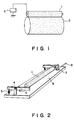
- FIG 1 shows an essential part of the electrophotographic apparatus according to the present invention.
- a charging member 1 having a roller form is disposed so that it contacts an electrophotographic photosensitive member 2, and the charging member 1 may charge the photosensitive member 2 on the basis of the voltage applied thereto from an external power supply 3 connected to the charging member 1.
- the form or shape of the charging member 1 may be, in addition to the above-mentioned roller form as shown in Figure 1, any of blade, belt, etc.
- the form of the charging member can appropriately be selected corresponding to the specifications and form of an electrophotographic apparatus.
- the material constituting the charging member 1 includes: metals such as aluminum, iron and copper; electroconductive polymer materials such as polyacetylene, polypyrrole and polythiophene; rubbers or artificial fibers supplied with electroconductivity, e.g., by dispersing therein electroconductive particles such as carbon and metal; and insulating material such as polycarbonate, polyvinyl chloride and polyester having a surface coated with a metal or another conductive material.
- At least the surface portion of the charging member 1 may preferably comprise an elastic or elastomeric material.
- the volume resistivity of the charging member 1 may preferably be 100 - 1012 ohm.cm, particularly 102 - 1010 ohm.cm.
- the contact pressure between the charging member and the photosensitive member may be about 100 g/cm or smaller, while it varies depending on the material and/or shape of the charging member.
- an abrasive is; one wherein the surface is mechanically ground by a sandblasting method, etc.; one wherein the surface is caused to have an orange peel-like form, e.g., by regulating the condition of drying to be effected after coating; one wherein the surface is exposed to a solvent; etc.
- the above-mentioned ten-point mean surface roughness (Rz2) of the charging member may be measured by using a universal surface shape-measuring machine (Model: SE-3C, mfd. by Kosaka Kenkyusho) according to Japanese Industrial Standard (JIS-B-0601).
- FIG 2 shows an embodiment of a charging unit for causing a charging member 1 to contact a photosensitive member (not shown) under pressure.
- the charging member 1 in the form of a roller is disposed so that it may contact the photosensitive member under pressure on the basis of the action of a supporting point 4 and a spring 5 which is disposed opposite to the charging member 1 by the medium of the supporting point 4.
- a core bar 6 is disposed in the central portion of the charging member 1, and supplied with a voltage by means of a feed brush 7 disposed in contact with the core bar 6.
- reference numeral 8 denotes a receiving connector for receiving a voltage from the apparatus body (not shown) and numeral 9 denotes a supporting member for supporting the charging member 1, which is disposed, e.g., along a guide rail (not shown) disposed on the apparatus body side.
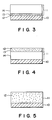
- FIGs 3, 4 and 5 show typical structures of the electrophotographic photosensitive member usable in the present invention, wherein the photosensitive layer comprises an organic photoconductor as a main component.
- the organic photoconductor may comprise an organic photoconductive polymer such as polyvinylcarbazole, or a binder resin containing therein a low-molecular weight organic photoconductive material.
- a photosensitive layer 11 is disposed on an electroconductive substrate 10.
- the photosensitive layer 11 comprises a charge generation layer 13 comprising a binder resin and a charge-generating substance 12 dispersed therein, and a charge transport layer 14 comprising a charge-transporting substance (not shown).
- the charge transport layer 14 is disposed on the charge generation layer 13.
- a charge transport layer 14 is disposed under a charge generation layer 13.
- the charge generation layer 13 can contain a charge-transporting substance, as desired.
- a photosensitive layer 11 is disposed on an electroconductive substrate 10.
- the photosensitive layer 11 comprises a binder resin and a charge-generating substance 12 and a charge-transporting substance (not shown) contained therein.
- the photosensitive member may preferably have a structure as shown in Figure 3, which comprises the electroconductive substrate 10, and the charge generation layer 13 and the charge transport layer 14 disposed in this order on the substrate 10.
- the electroconductive substrate 10 there may be used a cylindrical member, a sheet, a film, etc., of a material including metals such as aluminum and stainless steel, papers, plastics, etc.
- a layer of an electroconductive polymer, or a resinous layer containing electroconductive particles such as those of tin oxide, titanium oxide or silver.
- an undercoat layer (or adhesive layer) having a barrier function and an undercoat function.
- the undercoat layer may be formed as desired, for various purposes. These purposes may include: improvement in the adhesion or coating characteristic of the photosensitive layer, protection of the substrate, covering for the surface defect of the substrate, improvement in charge injection from the substrate, protection of the photosensitive layer from an electric breakdown, etc.
- the thickness of the undercoat layer may preferably be about 0.2 to 2 micrometres.
- the charge-generating substance there may be used, e.g., pyrilium or thiopyrylium dyes, phthalocyanine-type pigments, anthanthrone pigments; dibenzpyrene-quinone pigment, pyranthrone pigment, azo pigments, indigo pigments, quinacridone type pigments, quinocyanine compounds, asymmetric quinocyanine compounds, etc.
- the charge-transporting substance there may be used, e.g., hydrazone compounds, pyrazoline compounds, stilbene-type compounds, oxazole compounds, thiazole compounds, triarylmethane compounds, polyaryl alkanes, etc.
- the charge generation layer 13 e.g., the above-mentioned charge-generating substance and a binder resin, preferably in an amount of 0.5 - 4 times that of the charge-generating substance, are sufficiently dissolved or dispersed in a solvent by a dispersing means such as homogenizer, ultrasonic apparatus, ball mill, vibrating ball mill, sand mill, attritor or roll mill, and the resultant coating liquid may be applied onto a substrate, etc., and then dried.
- the charge generation layer 13 may preferably have a thickness of 5 microns or below, more preferably about 0.01 - 1 micrometres.
- the above-mentioned charge-transporting substance and a binder resin are dissolved or dispersed in a solvent, and the resultant coating liquid may be applied onto the charge generation layer, etc.
- the mixing ratio of the charge-transporting material to the binder resin may preferably be about 2:1 to 1:2.
- specific examples of the solvent may include: ketones such as acetone and methyl ethyl ketone; esters such as methyl acetate and ethyl acetate; aromatic hydrocarbons such as toluene and xylene; chlorohydrocarbons such as chlorobenzene, chloroform, and carbon tetrachloride, etc.
- the above-mentioned coating liquid there may be used various coating methods such as dip coating, spray coating, spinner coating.
- the drying may be conducted for a time in the range of 5 minutes to 5 hours preferably 10 minutes to 2 hours, at a temperature of 10 °C to 200 °C, preferably 20 °C - 150 °C, under quienscent condition or under blowing.
- the thus formed charge transport layer 14 may preferably have a thickness of about 5 - 30 microns, more preferably about 10 - 25 micrometres.
- binder resin used for the formation of the charge transport layer 14 may include; acrylic resins, styrene resins, polyesters, polycarbonates, polyacrylates, polysulfones, polyphenylene oxide resins, epoxy resins, polyurethane resins, alkyd resins, unsaturated resin, etc.
- preferred examples may be: polymethyl methacrylate, polystyrene, styrene-acrylonitrile copolymer, polycarbonate resin, or diallyl phthalate resin.
- charge transport layer and/or the charge generation layer used in the present invention may further contain various additives such as antioxidant, ultraviolet ray-absorbing agent and lubricant.
- the surface of the electrophotographic photosensitive member there may be used various methods including: one wherein the surface is mechanically ground by using an abrasive or by sandblasting; one wherein electrically inert particles such as metal oxide powder and resin powder are dispersed in the surface layer of a photosensitive member; etc.
- the ten-point mean surface roughness (Rz1) of the photosensitive member may be measured in the same manner as that in the case of the charging member.
- a photosensitive layer which is constituted so that its surface predominantly comprises a resin generally provides a smooth surface.
- a photosensitive member having such a smooth surface contacts a charging member having a smooth surface, the photosensitive member closely adheres to the charging member, whereby a surface defect of the photosensitive member is liable to occur due to peeling of the photosensitive layer.
- the photosensitive member and charging member may retain an appropriate contact state therebetween, whereby the above-mentioned problem does not occur.
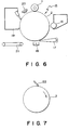
- Figure 6 shows an embodiment of the image forming apparatus using the electrophotographic apparatus according to the present invention.
- the image forming apparatus comprises: an electrophotographic photosensitive member 2, and around the peripheral surface of the photosensitive member 2, a charging member 1 in the form of a roller, an image exposure means (not shown) for providing a light beam 15 to form a latent image on the photosensitive member 2, a developing device 16 for developing the latent image with a toner or developer (not shown) to form a toner image on the photosensitive member 2, a transfer charger 18 for transferring the toner image from the photosensitive member 2 onto a transfer material (not shown), a cleaner 19 for removing a residual toner from the photosensitive member 2, and a pre-exposure means 20 for providing light to the photosensitive member 2.
- the image forming apparatus shown in Figure 6 further comprises a pair of paper feed rollers and a paper feed guide 17 for supplying the transfer material (or transfer-receiving material) such as paper to the photosensitive member 2.
- a voltage is applied to the charging member 1 disposed in contact with the photosensitive member 2, thereby to charge the surface of the photosensitive member 2, and the photosensitive member 2 is imagewise exposed to light 15 corresponding to an original image by the image exposure means, thereby to form an electrostatic latent image on the photosensitive member 2.
- the electrostatic latent image formed on the photosensitive member 2 is developed or visualized by attaching the toner or developer contained in the developing device 16 to form a toner image on the photosensitive member 2.
- the toner image is then transferred to the transfer material such as paper which has been supplied by means of the paper feed rollers and paper feed guide 17, by means of the transfer charger 18 to form a toner image on the transfer material.
- the residual toner which remains on the photosensitive member 2 without transferring to the transfer material at the time of transfer is recovered by means of the cleaner 19.
- the copied image is formed by such an electrophotographic process.
- the photosensitive member 2 may preferably be exposed to light by the pre-exposure means 20 to remove the residual charge, prior to the above-mentioned primary charging based on the charging member 1.
- the transfer material on which the above-mentioned toner image has been formed may be conveyed to a fixing unit (not shown) by means of a conveyor 21, whereby the toner image is fixed to the transfer material.
- the light source for providing light 15 for image exposure may be a halogen lamp, a fluorescent lamp, a laser, etc. Further, another auxiliary process may be included in the above-mentioned electrophotographic process, as desired.
- the voltage applied to the charging member 1 may be a DC voltage alone, but may preferably be a superposition of a DC voltage and an AC voltage in order to stably effect uniform charging.
- the DC voltage may appropriately be determined depending on an intended surface potential of the photosensitive member, but may preferably be ⁇ 400 V to ⁇ 1000 V, more preferably ⁇ 550 V to ⁇ 850 V.
- the AC voltage to be superposed on the DC voltage may preferably be 1800 V or lower, more preferably 1500 V or lower, in terms of peak-to-peak value (Vpp) of the alternating current voltage.
- the method for applying a voltage may include: one wherein a desired voltage is instantaneously applied; one wherein the applied voltage is gradually or stepwise raised in order to protect a photosensitive member; or one wherein a DC voltage and an AC voltage are applied in a sequence of from DC voltage to AC voltage, or of from AC voltage to DC voltage.
- the electrophotographic apparatus according to the present invention may be used not only for ordinary copying machines but also in the fields related to electrophotography such as laser-beam printers, CRT printers and electrophotographic plate-making.
- the thus prepared nine charging members were mechanically ground by using a lapping tape so that they provided ten-point mean surface roughnesses (Rz1) of 0 micrometres, 0.05 micrometres, 0.1 micrometres, 0.3 micrometres, 1.0 micrometres, 3.0 micrometres, 4.0 micrometres, 5.0 micrometres and 6.0 micrometres, respectively.
- Rz1 mean surface roughnesses
- an electrophotographic photosensitive member was prepared in the following manner.
- a 5 % solution of a polyamide resin (trade name: Amilan CM-8000, mfd. by Toray K.K.) in methanol was applied on a substrate of an aluminum cylinder having a diameter of 80 mm and a length of 360 mm by dip coating and then dried thereby to form a 1 micron-thick undercoat layer on the aluminum substrate.
- a polyamide resin trade name: Amilan CM-8000, mfd. by Toray K.K.
- a hydrazone compound represented by the following structural formula 7 parts of a hydrazone compound represented by the following structural formula and 10 parts of a polystyrene resin (trade name: Diarex HF-55, mfd. by Mitsubishi Monsanto Kasei K.K.), as a binder resin were dissolved in 50 parts of monochlorobenzene.
- a polystyrene resin trade name: Diarex HF-55, mfd. by Mitsubishi Monsanto Kasei K.K.
- the resultant solution was applied onto the above-mentioned charge generation layer and dried to form a 19 microns-thick charge transport layer, whereby a photosensitive member was obtained.
- the thus prepared seven charging members were mechanically ground so that they provided ten-point mean surface roughnesses (Rz2) of 0 micrometres, 0.05 micrometres, 0.1 micrometres, 0.3 micrometres, 1.0 micrometre, 3.0 micrometres and 5.0 micrometres, respectively.
- Rz2 mean surface roughnesses
- a successive copying test of 10,000 sheets (A-4 size) was conducted in an environment of 23 °C, 50 % RH by using an original having an image portion of 6 %.
- the image forming apparatus used herein comprised a modification of a copying machine (trade name: NP 3525, mfd. by Canon K.K.) wherein the image exposure means, developing device, paper feed system, transfer charger, conveyor system, and pre-exposure means were used as such.
- This modification used the above-mentioned charging member 1 in the form of a roller as the charging means, and had been modified so that it conducted cleaning by blade cleaning alone by using a cleaner comprising a silicone rubber blade.
- the voltage applied to the charging unit was a superposition of a DC voltage of -700 V and an AC voltage having a peak-to-peak voltage (Vpp) of 1500 V and a frequency of 1000 Hz.
- the results were evaluated by measuring the surface potential of the photosensitive member in the initial stage when it was charged by using the charging member, and the image densities of the copied images obtained before and after the successive copying of 10,000 sheets.
- the surface potential was measured by means of a surface potential meter (trade name. 244 Surface Potential Meter, mfd. by Monroe Electronics Inc.).
- the copied image was evaluated by measuring the reflection density of the solid black image portion by means of a Macbeth Reflection Densitometer (mfd. by Macbeth Co.).
- a plate-type blade 22 as shown in Figure 7 having a volume resistivity of 108 ohm.cm, a thickness of 2 mm, a height of 20 mm and a width of 330 mm was shaped by using the above-mentioned material used for shaping the roller charging member obtained in Example 1.
- the resultant blade 22 was assembled in the image forming apparatus in the same manner as in Example 1 except that the blade 22 was caused to contact the photosensitive member 2 so that it was disposed in the forward direction with respect to the moving direction of the photosensitive member 2 as shown in Figure 7.
- evaluation was conducted in the same manner as in Example 1.
- a photosensitive member was prepared in the same manner as in Example 1 except that a styrene-methyl methacrylate copolymer (trade name: Estyrene MS-300, mfd. by Shin-Nichitetsu Kagaku K.K.) was used as the binder resin of the charge transport layer instead of the polystyrene resin used in Example 1.
- a styrene-methyl methacrylate copolymer trade name: Estyrene MS-300, mfd. by Shin-Nichitetsu Kagaku K.K.
- the thus obtained photosensitive member was assembled in the image forming apparatus used in Example 1 together with the charging unit used in Example 1 and the resultant apparatus was used for evaluation of images in the same manner as in Example 1.
- the number of the dielectric breakdowns was the number of the white dropouts having a diameter of 1 mm or larger and white dropouts (or white streaks) having a width of 1 mm or larger and extending along a direction parallel to the longitudinal direction of the photosensitive member, which occurred in the solid black images portions.
- the combinations of the photosensitive member and charging member providing (Rz1 + Rz2) of 0.1 micrometres, 0.4 micrometres, 1.3 micrometres, 2.0 micrometres, 4.0 micrometres and 5.3 micrometres satisfying the conditions according to the present invention caused substantially no dielectric breakdown and provided good copied images.
Landscapes
- Physics & Mathematics (AREA)
- General Physics & Mathematics (AREA)
- Engineering & Computer Science (AREA)
- Plasma & Fusion (AREA)
- Electrostatic Charge, Transfer And Separation In Electrography (AREA)
- Photoreceptors In Electrophotography (AREA)
- Discharging, Photosensitive Material Shape In Electrophotography (AREA)
Applications Claiming Priority (4)
| Application Number | Priority Date | Filing Date | Title |
|---|---|---|---|
| JP276879/88 | 1988-10-31 | ||
| JP27687988 | 1988-10-31 | ||
| JP29751188 | 1988-11-24 | ||
| JP297511/88 | 1988-11-24 |
Publications (3)
| Publication Number | Publication Date |
|---|---|
| EP0367203A2 EP0367203A2 (en) | 1990-05-09 |
| EP0367203A3 EP0367203A3 (en) | 1991-06-12 |
| EP0367203B1 true EP0367203B1 (en) | 1993-07-21 |
Family
ID=26552151
Family Applications (1)
| Application Number | Title | Priority Date | Filing Date |
|---|---|---|---|
| EP89120136A Expired - Lifetime EP0367203B1 (en) | 1988-10-31 | 1989-10-30 | Electrophotographic apparatus |
Country Status (6)
| Country | Link |
|---|---|
| US (1) | US5008706A (ko) |
| EP (1) | EP0367203B1 (ko) |
| JP (1) | JP2584873B2 (ko) |
| KR (1) | KR920011089B1 (ko) |
| CN (1) | CN1024848C (ko) |
| DE (1) | DE68907689T2 (ko) |
Families Citing this family (55)
| Publication number | Priority date | Publication date | Assignee | Title |
|---|---|---|---|---|
| US5307122A (en) * | 1989-07-28 | 1994-04-26 | Canon Kabushiki Kaisha | Image forming apparatus apparatus unit facsimile apparatus and developer comprising hydrophobic silica fine powder for developing electrostatic images |
| DE69125406T2 (de) * | 1990-01-24 | 1997-10-30 | Canon Kk | Aufladegerät |
| EP0458273B1 (en) * | 1990-05-21 | 1997-08-13 | Canon Kabushiki Kaisha | Charging device, image forming apparatus with same and a process unit detachable mountable to the image forming apparatus |
| US5162183A (en) * | 1990-07-31 | 1992-11-10 | Xerox Corporation | Overcoat for imaging members |
| US5270768A (en) * | 1991-04-24 | 1993-12-14 | Canon Kabushiki Kaisha | Charging member containing reduced titanium oxide and device using same |
| JP3262346B2 (ja) * | 1991-07-31 | 2002-03-04 | キヤノン株式会社 | 帯電装置及び帯電装置を有するプロセスカートリッジ又は画像形成装置 |
| DE69220313T2 (de) * | 1991-09-27 | 1998-01-08 | Bridgestone Corp | Kontaktaufladegerät und Verfahren |
| US5786091A (en) * | 1991-12-02 | 1998-07-28 | Ricoh Company, Ltd. | Charge roller for an image forming apparatus |
| DE4244917C2 (de) * | 1991-12-02 | 2000-05-18 | Ricoh Kk | Ladevorrichtung zum Laden eines photoleitfähigen Elements und Verfahren zum Herstellen der Ladevorrichtung |
| JP2574107B2 (ja) * | 1991-12-02 | 1997-01-22 | 株式会社リコー | 帯電ローラ及びその製造方法,及び帯電ローラを用いた画像形成装置及びその帯電装置 |
| JP3320102B2 (ja) * | 1992-06-30 | 2002-09-03 | キヤノン株式会社 | プロセスカートリッジ及び画像形成装置 |
| EP0586965A3 (en) * | 1992-08-28 | 1994-10-12 | Canon Kk | Electrophotographic image forming method, electrophotographic apparatus and electrophotographic apparatus. |
| US5464721A (en) * | 1992-09-02 | 1995-11-07 | Fuji Xerox Co., Ltd. | Amorphous silicon photoreceptor and electrophotographic process using the same |
| US5485344A (en) * | 1992-09-28 | 1996-01-16 | Mita Industrial Co., Ltd. | Method of contact-charging the surface of a photosensitive material |
| JPH06194854A (ja) * | 1992-12-25 | 1994-07-15 | Konica Corp | 画像形成方法 |
| IT1267423B1 (it) * | 1993-03-17 | 1997-02-05 | Seiko Epson Corp | Apparecchio di carica |
| GB2287360B (en) * | 1993-03-17 | 1997-01-15 | Seiko Epson Corp | Charger apparatus |
| JP3400054B2 (ja) * | 1993-05-31 | 2003-04-28 | 株式会社リコー | 画像形成装置 |
| US5548380A (en) * | 1993-12-28 | 1996-08-20 | Matsushita Electric Industrial Co., Ltd. | Charging device and an image forming apparatus using a charging device |
| JPH0850393A (ja) * | 1994-08-05 | 1996-02-20 | Tec Corp | 画像形成装置のプロセスユニット |
| JPH0950170A (ja) * | 1994-10-19 | 1997-02-18 | Canon Inc | 帯電装置 |
| JP2827937B2 (ja) * | 1994-11-22 | 1998-11-25 | 富士ゼロックス株式会社 | 下引き層を有する電子写真感光体および電子写真装置 |
| US5740008A (en) * | 1995-04-18 | 1998-04-14 | Bridgestone Corporation | Charging member and device |
| KR0154707B1 (ko) * | 1995-09-19 | 1998-12-15 | 김광호 | 화상 형성 장치의 프로세서 카트리지 |
| US6278854B1 (en) * | 1997-03-31 | 2001-08-21 | Canon Kabushiki Kaisha | Electrophotographic apparatus and process cartridge |
| US6180302B1 (en) * | 1997-10-27 | 2001-01-30 | Canon Kabushiki Kaisha | Electrophotographic photosensitive member, and process cartridge and electrophotographic apparatus provided with the electrophotographic member |
| US6408152B1 (en) * | 1998-04-30 | 2002-06-18 | Canon Kabushiki Kaisha | Process cartridge and electrophotographic apparatus |
| US6620494B2 (en) * | 1999-07-03 | 2003-09-16 | Ten Cate Enbi B.V. | Conductive roller |
| JP2001249478A (ja) | 2000-03-02 | 2001-09-14 | Fuji Xerox Co Ltd | 画像形成装置、プロセスカートリッジ、及びそれらの再生方法 |
| JP2001337470A (ja) * | 2000-05-25 | 2001-12-07 | Canon Inc | 電子写真画像形成装置および電子写真画像形成方法 |
| DE60141562D1 (de) * | 2000-11-08 | 2010-04-29 | Ricoh Kk | Elektrophotographischer Photorezeptor, Verfahren zur Herstellung des Photorezeptors, und bildformendes Verfahren sowie Apparat worin der Photorezeptor eingesetzt wird |
| DE60229995D1 (de) * | 2001-05-01 | 2009-01-08 | Ricoh Kk | Elektrophotographischer Photorezeptor, Herstellungsverfahren und Bilderzeugungsvorrichtung |
| EP1324139A3 (en) * | 2001-12-06 | 2003-10-22 | Ricoh Company, Ltd. | Electrophotographic photoconductor, process cartridge, image forming apparatus and image forming method |
| US7232635B2 (en) * | 2002-02-04 | 2007-06-19 | Konica Corporation | Image forming method, image forming apparatus, and processing cartridge |
| JP4134576B2 (ja) * | 2002-02-28 | 2008-08-20 | コニカミノルタホールディングス株式会社 | 画像形成方法、画像形成装置及びプロセスカートリッジ |
| US7558507B2 (en) | 2002-03-26 | 2009-07-07 | Brother Kogyo Kabushiki Kaisha | Image forming apparatus, and pressure fogging prevention |
| JP4456951B2 (ja) * | 2004-07-16 | 2010-04-28 | 富士ゼロックス株式会社 | 画像形成装置及びプロセスカートリッジ |
| JP4456954B2 (ja) * | 2004-07-16 | 2010-04-28 | 富士ゼロックス株式会社 | 電子写真感光体、プロセスカートリッジおよび電子写真装置 |
| JP4456952B2 (ja) * | 2004-07-16 | 2010-04-28 | 富士ゼロックス株式会社 | 電子写真感光体、プロセスカートリッジおよび電子写真装置 |
| JP4456953B2 (ja) * | 2004-07-16 | 2010-04-28 | 富士ゼロックス株式会社 | 画像形成装置及びプロセスカートリッジ |
| JP4456955B2 (ja) * | 2004-07-16 | 2010-04-28 | 富士ゼロックス株式会社 | 電子写真感光体、電子写真用カートリッジおよび電子写真装置 |
| JP4649986B2 (ja) * | 2004-12-27 | 2011-03-16 | 富士ゼロックス株式会社 | 画像形成装置 |
| US20100183330A1 (en) * | 2007-06-12 | 2010-07-22 | Mitsubishi Chemical Corporation | Image-forming apparatus and cartridge |
| JP5194057B2 (ja) * | 2010-06-04 | 2013-05-08 | 京セラドキュメントソリューションズ株式会社 | 正帯電単層型電子写真感光体、及び画像形成装置 |
| US8628823B2 (en) * | 2011-06-16 | 2014-01-14 | Xerox Corporation | Methods and systems for making patterned photoreceptor outer layer |
| JP2013200417A (ja) * | 2012-03-23 | 2013-10-03 | Fuji Xerox Co Ltd | 電子写真感光体、プロセスカートリッジ、及び、画像形成装置 |
| US8765339B2 (en) * | 2012-08-31 | 2014-07-01 | Xerox Corporation | Imaging member layers |
| JP2014153456A (ja) * | 2013-02-06 | 2014-08-25 | Konica Minolta Inc | 画像形成方法 |
| US20140295333A1 (en) * | 2013-03-29 | 2014-10-02 | Xerox Corporation | Image forming system |
| US9690217B2 (en) * | 2014-08-28 | 2017-06-27 | Kyocera Document Solutions, Inc. | Triarylamine derivative, electrophotographic photosensitive member, and image forming apparatus |
| CN105384646B (zh) * | 2014-08-29 | 2018-06-29 | 京瓷办公信息系统株式会社 | 三苯胺衍生物、感光体和图像形成装置 |
| JP6421922B2 (ja) * | 2014-10-02 | 2018-11-14 | 株式会社リコー | 画像形成装置 |
| CN110637259A (zh) * | 2017-10-18 | 2019-12-31 | 富士电机株式会社 | 电子摄影用感光体、其制造方法以及电子摄影装置 |
| JP2020052165A (ja) * | 2018-09-26 | 2020-04-02 | キヤノン株式会社 | 画像形成装置 |
| JP2020052163A (ja) * | 2018-09-26 | 2020-04-02 | キヤノン株式会社 | 画像形成装置 |
Family Cites Families (21)
| Publication number | Priority date | Publication date | Assignee | Title |
|---|---|---|---|---|
| UST886015I4 (en) * | 1970-11-02 | 1971-05-11 | Flexible transparent contact charging element for electrophotography | |
| US4387980A (en) * | 1979-12-25 | 1983-06-14 | Tokyo Shibaura Denki Kabushiki Kaisha | Charging device for electronic copier |
| JPS56104350A (en) * | 1980-01-25 | 1981-08-20 | Toshiba Corp | Charging device of electrophotographic copier |
| JPS56104351A (en) * | 1980-01-25 | 1981-08-20 | Toshiba Corp | Charging device of electrophotographic copier |
| JPS56104352A (en) * | 1980-01-25 | 1981-08-20 | Toshiba Corp | Charging device of electrophotographic copier |
| DE3101678C2 (de) * | 1980-01-25 | 1983-07-07 | Tokyo Shibaura Denki K.K., Kawasaki, Kanagawa | Einrichtung zum gleichförmigen Aufladen eines kontinuierlich durch eine Aufladezone bewegten elektrofotografischen Aufzeichnungsmaterials |
| JPS56132356A (en) * | 1980-03-21 | 1981-10-16 | Minolta Camera Co Ltd | Roller charger |
| US4309803A (en) * | 1980-09-29 | 1982-01-12 | Xerox Corporation | Low cost foam roll for electrostatographic reproduction machine |
| JPS5767951A (en) * | 1980-10-14 | 1982-04-24 | Toshiba Corp | Electric charger |
| JPS57178267A (en) * | 1981-04-27 | 1982-11-02 | Fuji Xerox Co Ltd | Electrostatic charger for electrophotographic copier |
| JPS5840566A (ja) * | 1981-09-03 | 1983-03-09 | Kinoshita Kenkyusho:Kk | 電子写真の接触帯電方法 |
| JPS58139156A (ja) * | 1982-02-13 | 1983-08-18 | Canon Inc | 帯電方法 |
| JPS58150975A (ja) * | 1982-03-03 | 1983-09-07 | Canon Inc | 摺擦帯電装置 |
| JPS61123850A (ja) * | 1984-10-31 | 1986-06-11 | Canon Inc | 電子写真感光体及び画像形成法 |
| JPS61123848A (ja) * | 1984-11-21 | 1986-06-11 | Canon Inc | 電子写真感光体 |
| JPS6330850A (ja) * | 1986-07-24 | 1988-02-09 | Canon Inc | 電子写真感光体 |
| US4727453A (en) * | 1986-12-22 | 1988-02-23 | Xerox Corporation | Alternating current inductive charging of a photoreceptor |
| JPS63220161A (ja) * | 1987-03-10 | 1988-09-13 | Canon Inc | 電子写真感光体 |
| JPS63223751A (ja) * | 1987-03-13 | 1988-09-19 | Canon Inc | 電子写真感光体 |
| US4922299A (en) * | 1988-04-07 | 1990-05-01 | Unico Co., Ltd. | Electrostatic charge emitting apparatus |
| JPH01261675A (ja) * | 1988-04-13 | 1989-10-18 | Canon Inc | 電子写真用帯電方法及び電子写真用帯電装置 |
-
1989
- 1989-10-25 US US07/426,197 patent/US5008706A/en not_active Expired - Lifetime
- 1989-10-27 JP JP1280316A patent/JP2584873B2/ja not_active Expired - Lifetime
- 1989-10-30 EP EP89120136A patent/EP0367203B1/en not_active Expired - Lifetime
- 1989-10-30 DE DE89120136T patent/DE68907689T2/de not_active Expired - Lifetime
- 1989-10-31 KR KR1019890015722A patent/KR920011089B1/ko not_active Expired
- 1989-10-31 CN CN89108262A patent/CN1024848C/zh not_active Expired - Fee Related
Also Published As
| Publication number | Publication date |
|---|---|
| CN1024848C (zh) | 1994-06-01 |
| DE68907689T2 (de) | 1993-11-18 |
| DE68907689D1 (de) | 1993-08-26 |
| KR920011089B1 (ko) | 1992-12-26 |
| EP0367203A3 (en) | 1991-06-12 |
| US5008706A (en) | 1991-04-16 |
| JPH02222985A (ja) | 1990-09-05 |
| JP2584873B2 (ja) | 1997-02-26 |
| KR900006830A (ko) | 1990-05-09 |
| EP0367203A2 (en) | 1990-05-09 |
| CN1043206A (zh) | 1990-06-20 |
Similar Documents
| Publication | Publication Date | Title |
|---|---|---|
| EP0367203B1 (en) | Electrophotographic apparatus | |
| EP0329366B1 (en) | Charging member | |
| JP2847524B2 (ja) | 帯電装置 | |
| US5430527A (en) | Electrophotographic apparatus having cleaning width larger than charging width | |
| US5328790A (en) | Photoreceptor for use in contact charging method and image forming apparatus employing said photoreceptor | |
| US6324365B1 (en) | Electrophotographic photosensitive member, and process cartridge and electrophotographic apparatus employing the same | |
| JP2002082464A (ja) | 画像形成装置、画像形成方法及びプロセスカートリッジ | |
| JPH02148059A (ja) | 電子写真装置 | |
| JP3227230B2 (ja) | 電子写真装置 | |
| JP2894508B2 (ja) | 帯電用部材 | |
| JP2765662B2 (ja) | 帯電用部材 | |
| JPH09325668A (ja) | 電子写真用ユニット及び電子写真装置 | |
| JP3302106B2 (ja) | 電子写真プロセスおよびそれに用いられる電子写真感光体 | |
| JPH06222649A (ja) | 帯電装置 | |
| JP2765660B2 (ja) | 帯電用部材 | |
| JP3740354B2 (ja) | プロセスカートリッジ及び電子写真装置 | |
| JP2946114B2 (ja) | 帯電用部材 | |
| JP2614304B2 (ja) | 電子写真用帯電部材及びこの帯電部材を用いた電子写真装置 | |
| US6434351B2 (en) | Electrophotographic photosensitive member, and process cartridge and electrophotographic apparatus employing the same | |
| JP2866451B2 (ja) | 帯電用部材 | |
| JP2946116B2 (ja) | 帯電用部材 | |
| JP2894509B2 (ja) | 帯電用部材 | |
| JPH07281501A (ja) | 画像形成装置 | |
| JP2001100444A (ja) | 電子写真複写装置 | |
| JP2000338700A (ja) | 電子写真感光体、電子写真感光体の製造方法、プロセスカートリッジ及び電子写真装置 |
Legal Events
| Date | Code | Title | Description |
|---|---|---|---|
| PUAI | Public reference made under article 153(3) epc to a published international application that has entered the european phase |
Free format text: ORIGINAL CODE: 0009012 |
|
| 17P | Request for examination filed |
Effective date: 19891030 |
|
| AK | Designated contracting states |
Kind code of ref document: A2 Designated state(s): DE FR GB |
|
| PUAL | Search report despatched |
Free format text: ORIGINAL CODE: 0009013 |
|
| AK | Designated contracting states |
Kind code of ref document: A3 Designated state(s): DE FR GB |
|
| 17Q | First examination report despatched |
Effective date: 19920918 |
|
| GRAA | (expected) grant |
Free format text: ORIGINAL CODE: 0009210 |
|
| AK | Designated contracting states |
Kind code of ref document: B1 Designated state(s): DE FR GB |
|
| REF | Corresponds to: |
Ref document number: 68907689 Country of ref document: DE Date of ref document: 19930826 |
|
| ET | Fr: translation filed | ||
| PLBE | No opposition filed within time limit |
Free format text: ORIGINAL CODE: 0009261 |
|
| STAA | Information on the status of an ep patent application or granted ep patent |
Free format text: STATUS: NO OPPOSITION FILED WITHIN TIME LIMIT |
|
| 26N | No opposition filed | ||
| REG | Reference to a national code |
Ref country code: GB Ref legal event code: IF02 |
|
| PGFP | Annual fee paid to national office [announced via postgrant information from national office to epo] |
Ref country code: DE Payment date: 20081031 Year of fee payment: 20 |
|
| PGFP | Annual fee paid to national office [announced via postgrant information from national office to epo] |
Ref country code: FR Payment date: 20081024 Year of fee payment: 20 |
|
| PGFP | Annual fee paid to national office [announced via postgrant information from national office to epo] |
Ref country code: GB Payment date: 20081029 Year of fee payment: 20 |
|
| REG | Reference to a national code |
Ref country code: GB Ref legal event code: PE20 Expiry date: 20091029 |
|
| PG25 | Lapsed in a contracting state [announced via postgrant information from national office to epo] |
Ref country code: GB Free format text: LAPSE BECAUSE OF EXPIRATION OF PROTECTION Effective date: 20091029 |