EP0369406A2 - Démodulateur cohérent pour modulation à déplacement de phase utilisant le taux d'erreur de bits et le rapport signal/bruit pour établir la synchronisation - Google Patents
Démodulateur cohérent pour modulation à déplacement de phase utilisant le taux d'erreur de bits et le rapport signal/bruit pour établir la synchronisation Download PDFInfo
- Publication number
- EP0369406A2 EP0369406A2 EP89121080A EP89121080A EP0369406A2 EP 0369406 A2 EP0369406 A2 EP 0369406A2 EP 89121080 A EP89121080 A EP 89121080A EP 89121080 A EP89121080 A EP 89121080A EP 0369406 A2 EP0369406 A2 EP 0369406A2
- Authority
- EP
- European Patent Office
- Prior art keywords
- signal
- frequency
- convolutional
- psk
- detected
- Prior art date
- Legal status (The legal status is an assumption and is not a legal conclusion. Google has not performed a legal analysis and makes no representation as to the accuracy of the status listed.)
- Granted
Links
Images


Classifications
-
- H—ELECTRICITY
- H04—ELECTRIC COMMUNICATION TECHNIQUE
- H04L—TRANSMISSION OF DIGITAL INFORMATION, e.g. TELEGRAPHIC COMMUNICATION
- H04L27/00—Modulated-carrier systems
- H04L27/18—Phase-modulated carrier systems, i.e. using phase-shift keying
- H04L27/22—Demodulator circuits; Receiver circuits
- H04L27/227—Demodulator circuits; Receiver circuits using coherent demodulation
- H04L27/2271—Demodulator circuits; Receiver circuits using coherent demodulation wherein the carrier recovery circuit uses only the demodulated signals
- H04L27/2273—Demodulator circuits; Receiver circuits using coherent demodulation wherein the carrier recovery circuit uses only the demodulated signals associated with quadrature demodulation, e.g. Costas loop
-
- H—ELECTRICITY
- H04—ELECTRIC COMMUNICATION TECHNIQUE
- H04L—TRANSMISSION OF DIGITAL INFORMATION, e.g. TELEGRAPHIC COMMUNICATION
- H04L27/00—Modulated-carrier systems
- H04L27/18—Phase-modulated carrier systems, i.e. using phase-shift keying
- H04L27/186—Phase-modulated carrier systems, i.e. using phase-shift keying in which the information is carried by both the individual signal points and the subset to which the individual signal points belong, e.g. coset coding or related schemes
-
- H—ELECTRICITY
- H04—ELECTRIC COMMUNICATION TECHNIQUE
- H04L—TRANSMISSION OF DIGITAL INFORMATION, e.g. TELEGRAPHIC COMMUNICATION
- H04L27/00—Modulated-carrier systems
- H04L27/0014—Carrier regulation
- H04L2027/0044—Control loops for carrier regulation
- H04L2027/0063—Elements of loops
- H04L2027/0067—Phase error detectors
-
- H—ELECTRICITY
- H04—ELECTRIC COMMUNICATION TECHNIQUE
- H04L—TRANSMISSION OF DIGITAL INFORMATION, e.g. TELEGRAPHIC COMMUNICATION
- H04L27/00—Modulated-carrier systems
- H04L27/0014—Carrier regulation
- H04L2027/0044—Control loops for carrier regulation
- H04L2027/0071—Control of loops
- H04L2027/0073—Detection of synchronisation state
-
- H—ELECTRICITY
- H04—ELECTRIC COMMUNICATION TECHNIQUE
- H04L—TRANSMISSION OF DIGITAL INFORMATION, e.g. TELEGRAPHIC COMMUNICATION
- H04L27/00—Modulated-carrier systems
- H04L27/0014—Carrier regulation
- H04L2027/0083—Signalling arrangements
- H04L2027/0089—In-band signals
- H04L2027/0093—Intermittant signals
Definitions
- the present invention relates generally to coherent PSK (phase shift keying) demodulators for M-ary PSK modulated convolutional codes, and more specifically, the present invention relates to a technique for recovering a carrier from a received PSK modulated convolutional code by precisely establishing synchronization with the received signal.
- PSK phase shift keying
- the received signal is mixed with a local carrier to produce I- and Q-channel signals for coupling to a convolutional decoder and phase comparison is made between the demodulated signal and the local carrier to establish carrier synchronization.
- synchronization is established between the frequency of the recovered carrier and the symbol rate of received convolutional codes by detecting the error rate of the demodulate I- and Q-channel signals and reducing the error rate below a specified value through a feedback circuit.
- a convolutional encoder is coupled to a convolution decoder.
- the output of the convolutional encoder and one input of the convolutional decoder are supplied to a correlator to determine their correlation. Since the output of the convolutional encoder is a replica of the original codeword, the correlator produces a signal which increases in amplitude with the error rate of the signal at the input of the convolutional decoder.
- a maximum detector is connected to the correlator to control the phase relation of the input signals of the convolutional decoder when the error rate exceeds a specified value.
- the prior art technique tends to establish carrier synchronization even when the carrier frequency is not precisely coherent with the symbol rate of the received signal. Under this condition, the demodulator is said to be in a "quasi-coherent" state.
- the demodulated data streams become equal to C n 171 and C n 133 and by decoding such data stream by an error correction circuit, or convolutional decoder, the original data D n can be recovered.
- the demodulated data streams will become C n 171′ and C n 133′ and the following relations will hold between error corrected data D′ n and the original data stream D n : Therefore, a decoding process properly proceeds and a decision is made that synchronization has been established.
- Bit-parallel codewords C n 171 and C n 133 are converted to bit-serial data and supplied to a BPSK modulator producing the following data B m :
- the demodulator produces bit-serial demodulated codewords B′ m which are converted to bit-parallel codewords. If the codewords B′ m have the following relations with the transmit data B′ m data streams C n 171′ and C n 133′ will result from a demodulation process.
- the demodulated data stream B ⁇ m will be given as follows if the frequency of the recovered carrier deviates as much as f s /4, where f s is the symbol rate of the transmitted signal:
- the value B ⁇ m is equal to B′ m if binary levels are used for discrimination between a valid coherent state and a quasi-coherent state. Even if the frequency of the recovered carrier deviates by as small as 1/8 of the symbol rate, a quasi-coherent state can occur.
- the coherent PSK demodulator comprises a PSK detector for demodulating a received PSK modulated convolutional code with a carrier generated by a variable frequency oscillator to produce demodulated convolutional codes of first and second channels.
- the oscillator is controlled in accordance with a phase control signal derived from the demodulated codes and further controlled in accordance with a frequency control signal.
- a convolutional decoder is provided for decoding the demodulated convolutional codes while correcting bit errors therein.
- An error rate detector is connected to the convolutional decoder for detecting when bit errors which occur during a specified period of time are smaller than a predetermined value to generate an output signal indicating that the convolutional decoder is synchronized with the demodulated convolutional codes.
- a power detector is connected to the PSK detector for detecting power levels of a signal component and a noise component of one of the first and second channels.
- a frequency control circuit is provided for performing the steps of (a) successively generating frequency control signals of a different value in response to an output signal from the error rate detector to cause the oscillator to generate a carrier of successively different frequencies as candidates for valid synchronization, (b) successively deriving signal-to-noise ratios from the detected power levels which result from the demodulation of the received PSK modulated convolutional code with the carrier of the different frequencies, and (c) detecting a maximum value of the derived signal-to-noise ratios to adopt one of the frequency control signals which corresponds to the detected maximum signal-to-noise ratio.
- the frequency control circuit repeats the steps (a), (b) and (c) to derive a plurality of frequency control signals as candidates for a most likelihood control parameter, detects two of the candidates having an equal value, and generates a frequency control signal corresponding to the detected candidates.
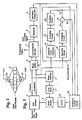
- the demodulator comprises a PSK detector 1 by which a received M-ary PSK signal is demodulated into an in-phase, or I-channel signal and a quadrature signal, or Q-channel signal.
- the demodulated signals supplied to a phase detector 2 where a phase difference between the I- and Q-channel signals is detected and supplied through a loop filter 3 to a variable phase shifter 4 to introduce a variable amount of delay to a carrier supplied from a voltage controlled oscillator 5 in accordance with the detected phase difference.
- the I- and Q-channel signals also are supplied through a phase shifter 6 to a convolutional decoder, or forward error correction (FEC) decoder 7 such as Viterbi decoder.
- FEC decoder 7 includes a copy of the convolutional encoder to decode the convolutional codes of both channels to generate a replica of the original data stream as a demodulator output in a known manner.
- the error correction signal which is generated for the decoding process, is supplied to an integrator 8.
- the output of integrator 8 will increase as the error rate of the demodulated signals increase and hence it increases as a function of the amount of deviation of the recovered carrier frequency from the symbol rate of the received signal.
- a threshold comparator 9 is connected to the output of integrator 8 to generate a logical-1 output when the integrator output exceeds a predetermined threshold level.
- the logical-1 output thus indicates that a substantial amount of bit errors exists in the demodulated signals and hence it gives an indication that VCO 5 is not in synchronization with the symbol rate of the received PSK signal.
- threshold comparator 9 is supplied to the phase shifter 6 which may comprise a switch to establish "through" connections between the outputs of PSK detector 1 and FEC decoder 7 in the presence of a logical-0 output from the threshold comparator 9 and establish cross-coupled connections between them in response to a logical-1 output from comparator 9 so that FEC decoder 7 reestablishes synchronization with the demodulated signals.
- the output of comparator 9 is applied to a frequency control circuit 11 which supplies a frequency control voltage to the VCO 5.
- frequency control circuit 10 interprets it as an indication that FEC decoder 7 is in synchronism with the demodulated signals and proceeds to compute the signal-to-noise ratio of the received PSK signal in a manner as will be described in detail hereinbelow.
- a power detector 11 is connected to one of the outputs of PSK detector 1.
- Power detector 11 comprises an absolute value converter 12 which converts the Q-channel signal to a signal having an absolute value, which is averaged by an averaging circuit 13.
- the output of averaging circuit 13 is squared by a squaring circuit 14 to supply a signal P S representative of the power level of the signal component to frequency control circuit 10.
- the Q-channel output is also squared by a squaring circuit 15 whose output is averaged by an averaging circuit 16 to provide a signal P T representative of the total power level of both signal and noise components.
- the power representative signals P S and P T are supplied to a subtractor 17 to provide the frequency control circuit 10 with an output signal P N representative of the power level of the noise component.
- Frequency control circuit 10 is a microprocessor-based controller having programmed steps as shown in Fig. 3.
- Program execution starts with operations block 30 which directs the sweeping of frequency control voltage V by incrementing it by a predetermined amount ⁇ V .
- decision block 31 which checks to see if there is a logical-0 input from threshold comparator 9 indicating that FEC decoder 7 is synchronized with the demodulated signals. If the answer is negative, blocks 30 and 31 are repeated until synchronization is established in decoder 7 by the closed-loop synchronizer formed by phase shifter 6, integrator 7 and threshold comparator 9.
- the VCO control voltage is swept across a range of voltages in search of synchronization.
- control proceeds to operations block 32 which directs the initialization of a variable i to one.
- the initialization step is followed by operations block 33 which directs the setting of the control voltage V to a voltage V i which is one of a plurality of voltage levels stored in a lookup table as corresponding to possible frequency values, or candidate lock points at which the demodulator is likely to be synchronized with the symbol rate of the incoming PSK signal. Therefore, VCO 5 is driven at one of the candidate voltages, and the demodulator is synchronized with the symbol rate of the incoming signal in a lock point which may be either false or valid.
- Block 34 which directs the computing of the formula 10 log10 (P S /P N ) using the power level signals P S and P N supplied from power detector 11 to derive the signal-to-noise ratio S/N of that lock point.
- the signal-to-ratio value S/N derived in step 34 is stored in a location of the lookup table adjacent the corresponding candidate voltage V i to form with it a data set DS (block 35).
- control exit is to block 37 which increments the variable i by one and control returns to block 33 to set the control voltage V to the next candidate by selecting one from the lookup table. In this way, the VCO frequency is successively shifted from one candidate frequency value to another so that the demodulator is successively synchronized in different lock points.
- control exits from decision block 36 to operations block 38 which directs the detecting of data set DS having a maximum value of the signal-to-noise ratios stored in the lookup table, and proceeds to block 39 to set the control voltage V to the candidate voltage V i at which the maximum signal-to-noise ratio is derived. Synchronization that occurs at the lock point having the maximum signal-to-noise ratio is interpreted as a valid lock and synchronizations at all the other lock points are interpreted as false locks.
- frequency control circuit 10 is further programmed to repeat the process of Fig. 3 as shown in Fig. 4 to determine whether the lock point detected in a manner described above is one that occurs at a most likelihood frequency.
- This program starts with an initialization step 40 which directs the setting of a variable n to one.
- Control exits to block 41 to execute the frequency control subroutine of Fig. 3 to derive a frequency control voltage V(1) .
- This voltage is stored in a memory (block 42) and control proceeds to block 43 to increment the variable n by one.
- the frequency control subroutine is repeated (block 44) to derive another frequency control voltage V(n) which is stored in the memory (block 45).
Landscapes
- Engineering & Computer Science (AREA)
- Computer Networks & Wireless Communication (AREA)
- Signal Processing (AREA)
- Digital Transmission Methods That Use Modulated Carrier Waves (AREA)
Applications Claiming Priority (2)
| Application Number | Priority Date | Filing Date | Title |
|---|---|---|---|
| JP63288344A JPH0748750B2 (ja) | 1988-11-15 | 1988-11-15 | 同期復調装置 |
| JP288344/88 | 1988-11-15 |
Publications (3)
| Publication Number | Publication Date |
|---|---|
| EP0369406A2 true EP0369406A2 (fr) | 1990-05-23 |
| EP0369406A3 EP0369406A3 (fr) | 1992-01-22 |
| EP0369406B1 EP0369406B1 (fr) | 1996-08-28 |
Family
ID=17728988
Family Applications (1)
| Application Number | Title | Priority Date | Filing Date |
|---|---|---|---|
| EP89121080A Expired - Lifetime EP0369406B1 (fr) | 1988-11-15 | 1989-11-14 | Démodulateur cohérent pour modulation à déplacement de phase utilisant le taux d'erreur de bits et le rapport signal/bruit pour établir la synchronisation |
Country Status (4)
| Country | Link |
|---|---|
| US (1) | US5157694A (fr) |
| EP (1) | EP0369406B1 (fr) |
| JP (1) | JPH0748750B2 (fr) |
| DE (1) | DE68927039T2 (fr) |
Cited By (9)
| Publication number | Priority date | Publication date | Assignee | Title |
|---|---|---|---|---|
| EP0497433A3 (en) * | 1987-06-23 | 1992-09-23 | Nec Corporation | Phase controlled demodulation system for digital communication |
| EP0504905A3 (en) * | 1991-03-20 | 1993-06-23 | Nec Corporation | Carrier recovery control with sequential fec sync detection and frame sync detection |
| EP0601855A3 (fr) * | 1992-12-09 | 1995-04-19 | Japan Radio Co Ltd | Egaliseur adaptatif, capable de compenser un décalage de la fréquence porteuse. |
| GB2303278A (en) * | 1995-07-11 | 1997-02-12 | Remo Giovanni Andrea Marzolini | Adaptive angle demodulation systems |
| EP0828366A2 (fr) * | 1996-08-09 | 1998-03-11 | Nec Corporation | Récupération de la porteuse dans un récepteur MAQ |
| AU715224B2 (en) * | 1996-02-27 | 2000-01-20 | Mitsubishi Denki Kabushiki Kaisha | A demodulator of receiver used for communications |
| EP0732021A4 (fr) * | 1993-12-03 | 2000-07-05 | Scientific Atlanta | Procede et appareil pour localiser et suivre une porteuse a mdpk |
| US6208201B1 (en) | 1998-02-28 | 2001-03-27 | Tandberg Television Asa | Recovery of a carrier signal from a modulated input signal |
| EP1524772A1 (fr) * | 2003-10-13 | 2005-04-20 | STMicroelectronics S.r.l. | Méthode et système de recouvrement de phase et de décodage |
Families Citing this family (24)
| Publication number | Priority date | Publication date | Assignee | Title |
|---|---|---|---|---|
| JP2673389B2 (ja) * | 1991-03-07 | 1997-11-05 | 松下電器産業株式会社 | データ伝送装置 |
| JP2932861B2 (ja) * | 1992-10-13 | 1999-08-09 | 日本電気株式会社 | 位相同期検出回路 |
| US5376894A (en) * | 1992-12-31 | 1994-12-27 | Pacific Communication Sciences, Inc. | Phase estimation and synchronization using a PSK demodulator |
| US5400363A (en) * | 1993-05-07 | 1995-03-21 | Loral Aerospace Corp. | Quadrature compensation for orthogonal signal channels |
| JP3106818B2 (ja) * | 1993-11-29 | 2000-11-06 | 株式会社村田製作所 | ディジタル無線受信方法および装置 |
| JPH07212421A (ja) * | 1994-01-19 | 1995-08-11 | Toshiba Corp | Afc回路 |
| US5457716A (en) * | 1994-01-31 | 1995-10-10 | Motorola, Inc. | Automatic frequency control in a radio communication receiver |
| US5432819A (en) * | 1994-03-09 | 1995-07-11 | Martin Marietta Corporation | DPSK communications with Doppler compensation |
| DE69528255T2 (de) * | 1994-04-08 | 2003-08-07 | Echelon Corp., Palo Alto | Verfahren und gerät zur sicheren winkelmodulationsbasierten kommunikation |
| US5692014A (en) * | 1995-02-03 | 1997-11-25 | Trw Inc. | Subsampled carrier recovery for high data rate demodulators |
| GB9521739D0 (en) * | 1995-10-24 | 1996-01-03 | Nat Transcommunications Ltd | Decoding carriers encoded using orthogonal frequency division multiplexing |
| JP2850949B2 (ja) * | 1995-12-15 | 1999-01-27 | 日本電気株式会社 | デジタルpll装置 |
| US5867503A (en) * | 1996-01-30 | 1999-02-02 | Mitsubishi Denki Kabushiki Kaisha | Digital sound broadcasting receiver and automatic phase controlling method therefor |
| JPH09321736A (ja) * | 1996-05-27 | 1997-12-12 | Sony Corp | 受信方法及び受信装置 |
| FR2753856B1 (fr) * | 1996-09-23 | 1998-12-18 | Procede et dispositif de detection de l'erreur sur la frequence d'une porteuse | |
| JP3392028B2 (ja) * | 1997-11-28 | 2003-03-31 | 株式会社ケンウッド | 階層化伝送ディジタル復調器 |
| US6430237B1 (en) * | 1998-11-16 | 2002-08-06 | Transamerica Business Credit Corporation | Method for accurate signal-to-interference measurement for wireless communication receivers |
| KR100333704B1 (ko) | 1999-06-21 | 2002-04-24 | 박종섭 | 위상잡음에 따른 위상회전오류 극복을 위한 결정영역 수정회로 |
| US6516036B1 (en) * | 1999-12-15 | 2003-02-04 | Sarnoff Corporation | Method and apparatus for decimating an oversampled signal |
| US7076001B2 (en) | 2001-10-16 | 2006-07-11 | Harris Corporation | System and method for an in-service decision-directed signal to noise ratio estimator |
| KR100556399B1 (ko) * | 2003-12-01 | 2006-03-03 | 엘지전자 주식회사 | Oob qpsk 수신기의 반송파 복구 장치 |
| ATE515109T1 (de) * | 2006-12-29 | 2011-07-15 | Motorola Mobility Inc | Verfahren und vorrichtung zur zwischenfrequenzauswahl |
| US8693968B2 (en) * | 2007-01-22 | 2014-04-08 | Freescale Semiconductor, Inc. | Very low intermediate frequency (VLIF) receiver |
| US8204156B2 (en) * | 2008-12-31 | 2012-06-19 | Intel Corporation | Phase error detection with conditional probabilities |
Family Cites Families (9)
| Publication number | Priority date | Publication date | Assignee | Title |
|---|---|---|---|---|
| JPS6025938B2 (ja) * | 1977-04-15 | 1985-06-21 | 日本電気株式会社 | 基準搬送波再生回路における擬似引込回避回路 |
| US4726029A (en) * | 1985-09-10 | 1988-02-16 | Hycom Incorporated | Error-correcting modem |
| JPS62159559A (ja) * | 1986-01-06 | 1987-07-15 | Nec Corp | 復調器制御方式 |
| JPH0810879B2 (ja) * | 1986-02-20 | 1996-01-31 | 富士通株式会社 | 復調装置 |
| US4837766A (en) * | 1986-03-24 | 1989-06-06 | Nec Corporation | Frame step-out detecting system |
| US4945549A (en) * | 1986-11-13 | 1990-07-31 | The United States Of America As Represented By The Administrator Of The National Aeronautics And Space Administration | Trellis coded modulation for transmission over fading mobile satellite channel |
| FR2614155A1 (fr) * | 1987-04-14 | 1988-10-21 | Thomson Csf | Indicateur numerique d'accrochage d'une boucle a verrouillage de phase de type costas |
| JPH0626353B2 (ja) * | 1987-05-19 | 1994-04-06 | 日本電気株式会社 | 復調装置 |
| DE3854505T2 (de) * | 1987-06-23 | 1996-02-22 | Nippon Electric Co | Phasengesteuerte Demodulationseinrichtung zur digitalen Kommunikation. |
-
1988
- 1988-11-15 JP JP63288344A patent/JPH0748750B2/ja not_active Expired - Lifetime
-
1989
- 1989-11-14 EP EP89121080A patent/EP0369406B1/fr not_active Expired - Lifetime
- 1989-11-14 DE DE68927039T patent/DE68927039T2/de not_active Expired - Lifetime
-
1992
- 1992-01-17 US US07/824,716 patent/US5157694A/en not_active Expired - Lifetime
Cited By (13)
| Publication number | Priority date | Publication date | Assignee | Title |
|---|---|---|---|---|
| EP0497433A3 (en) * | 1987-06-23 | 1992-09-23 | Nec Corporation | Phase controlled demodulation system for digital communication |
| EP0504905A3 (en) * | 1991-03-20 | 1993-06-23 | Nec Corporation | Carrier recovery control with sequential fec sync detection and frame sync detection |
| US5229997A (en) * | 1991-03-20 | 1993-07-20 | Nec Corporation | Carrier recovery control with sequential fec sync detection and frame sync detection |
| EP0601855A3 (fr) * | 1992-12-09 | 1995-04-19 | Japan Radio Co Ltd | Egaliseur adaptatif, capable de compenser un décalage de la fréquence porteuse. |
| US5499268A (en) * | 1992-12-09 | 1996-03-12 | Japan Radio Co., Ltd. | Adaptive equalizer capable of compensating for carrier frequency offset |
| EP0732021A4 (fr) * | 1993-12-03 | 2000-07-05 | Scientific Atlanta | Procede et appareil pour localiser et suivre une porteuse a mdpk |
| GB2303278B (en) * | 1995-07-11 | 2000-04-26 | Remo Giovanni Andrea Marzolini | Improvements to demodulation systems |
| GB2303278A (en) * | 1995-07-11 | 1997-02-12 | Remo Giovanni Andrea Marzolini | Adaptive angle demodulation systems |
| AU715224B2 (en) * | 1996-02-27 | 2000-01-20 | Mitsubishi Denki Kabushiki Kaisha | A demodulator of receiver used for communications |
| EP0828366A2 (fr) * | 1996-08-09 | 1998-03-11 | Nec Corporation | Récupération de la porteuse dans un récepteur MAQ |
| US6208201B1 (en) | 1998-02-28 | 2001-03-27 | Tandberg Television Asa | Recovery of a carrier signal from a modulated input signal |
| EP1524772A1 (fr) * | 2003-10-13 | 2005-04-20 | STMicroelectronics S.r.l. | Méthode et système de recouvrement de phase et de décodage |
| US7424068B2 (en) | 2003-10-13 | 2008-09-09 | Stmicroelectronics S.R.L. | Method and system for coding/decoding signals and computer program product therefor |
Also Published As
| Publication number | Publication date |
|---|---|
| JPH0748750B2 (ja) | 1995-05-24 |
| EP0369406B1 (fr) | 1996-08-28 |
| EP0369406A3 (fr) | 1992-01-22 |
| US5157694A (en) | 1992-10-20 |
| DE68927039D1 (de) | 1996-10-02 |
| JPH02134044A (ja) | 1990-05-23 |
| DE68927039T2 (de) | 1997-01-16 |
Similar Documents
| Publication | Publication Date | Title |
|---|---|---|
| EP0369406B1 (fr) | Démodulateur cohérent pour modulation à déplacement de phase utilisant le taux d'erreur de bits et le rapport signal/bruit pour établir la synchronisation | |
| US5012491A (en) | Preamable detection circuit for digital communications system | |
| EP0380876B1 (fr) | Décodeur à probabilité maximale synchrone en phase | |
| US5229997A (en) | Carrier recovery control with sequential fec sync detection and frame sync detection | |
| JPH021675A (ja) | オフセットqpsk方式用の搬送波再生回路 | |
| US4764730A (en) | Radio receiver demodulation system | |
| GB2295071A (en) | Coherent phase-shift keying detector | |
| JP2634319B2 (ja) | コヒーレント無線受信機の周波数制御方法及びその方法を実施する装置 | |
| EP0504890A2 (fr) | Démodulateur pour démoduler un signal modulé différentiellement en quadrature de phase avec déphasage de pi/4 | |
| EP0692895A2 (fr) | Démodulateur utilisant une détection différentielle | |
| CA1081364A (fr) | Systeme de detection differentielle a correction d'erreur non redondante | |
| US5313493A (en) | Plural-differential, phase-shift-keyed modulation, communication system | |
| US6778589B1 (en) | Symbol synchronous device and frequency hopping receiver | |
| US5448201A (en) | Clock recovery circuit in π/4 shift quadriphase PSK demodulator | |
| US7046743B2 (en) | Demodulator for demodulating digital modulated signals | |
| EP0695042A2 (fr) | Méthode de décodage et décodeur Viterbi capable de résoudre d'indétermination de phase | |
| US6597725B1 (en) | Carrier phase follower and frequency hopping receiver | |
| EP0618707B1 (fr) | Dispositif d'élimination d'ambiguité de phase | |
| JPH06120995A (ja) | ディジタル無線用受信機のフレーム同期回路 | |
| US5841815A (en) | Data receiver for correcting a phase of a received phase-modulated signal | |
| JPH06350660A (ja) | 復調装置 | |
| JP2800855B2 (ja) | ディジタル無線通信方式 | |
| US6925136B1 (en) | Simultaneous frequency and phase synchronizer | |
| KR100261226B1 (ko) | 파이/4 차분 직교위상 변조신호의 기저대역 차분 검파기 | |
| Serizawa et al. | Phase‐tracking viterbi demodulator |
Legal Events
| Date | Code | Title | Description |
|---|---|---|---|
| PUAI | Public reference made under article 153(3) epc to a published international application that has entered the european phase |
Free format text: ORIGINAL CODE: 0009012 |
|
| 17P | Request for examination filed |
Effective date: 19891208 |
|
| AK | Designated contracting states |
Kind code of ref document: A2 Designated state(s): DE FR GB IT NL |
|
| PUAL | Search report despatched |
Free format text: ORIGINAL CODE: 0009013 |
|
| AK | Designated contracting states |
Kind code of ref document: A3 Designated state(s): DE FR GB IT NL |
|
| 17Q | First examination report despatched |
Effective date: 19940104 |
|
| GRAH | Despatch of communication of intention to grant a patent |
Free format text: ORIGINAL CODE: EPIDOS IGRA |
|
| GRAA | (expected) grant |
Free format text: ORIGINAL CODE: 0009210 |
|
| GRAH | Despatch of communication of intention to grant a patent |
Free format text: ORIGINAL CODE: EPIDOS IGRA |
|
| AK | Designated contracting states |
Kind code of ref document: B1 Designated state(s): DE FR GB IT NL |
|
| REF | Corresponds to: |
Ref document number: 68927039 Country of ref document: DE Date of ref document: 19961002 |
|
| ET | Fr: translation filed | ||
| ITF | It: translation for a ep patent filed | ||
| PLBE | No opposition filed within time limit |
Free format text: ORIGINAL CODE: 0009261 |
|
| STAA | Information on the status of an ep patent application or granted ep patent |
Free format text: STATUS: NO OPPOSITION FILED WITHIN TIME LIMIT |
|
| 26N | No opposition filed | ||
| REG | Reference to a national code |
Ref country code: GB Ref legal event code: IF02 |
|
| PGFP | Annual fee paid to national office [announced via postgrant information from national office to epo] |
Ref country code: NL Payment date: 20081116 Year of fee payment: 20 Ref country code: DE Payment date: 20081107 Year of fee payment: 20 |
|
| PGFP | Annual fee paid to national office [announced via postgrant information from national office to epo] |
Ref country code: IT Payment date: 20081126 Year of fee payment: 20 |
|
| PGFP | Annual fee paid to national office [announced via postgrant information from national office to epo] |
Ref country code: FR Payment date: 20081112 Year of fee payment: 20 |
|
| PGFP | Annual fee paid to national office [announced via postgrant information from national office to epo] |
Ref country code: GB Payment date: 20081112 Year of fee payment: 20 |
|
| REG | Reference to a national code |
Ref country code: GB Ref legal event code: PE20 Expiry date: 20091113 |
|
| NLV7 | Nl: ceased due to reaching the maximum lifetime of a patent |
Effective date: 20091114 |
|
| PG25 | Lapsed in a contracting state [announced via postgrant information from national office to epo] |
Ref country code: NL Free format text: LAPSE BECAUSE OF EXPIRATION OF PROTECTION Effective date: 20091114 |
|
| PG25 | Lapsed in a contracting state [announced via postgrant information from national office to epo] |
Ref country code: GB Free format text: LAPSE BECAUSE OF EXPIRATION OF PROTECTION Effective date: 20091113 |