EP0373344A2 - Verfahren zum Herstellen von Leiterbahnen innerhalb eines isolierenden Substrates Isolierendensubstrat - Google Patents
Verfahren zum Herstellen von Leiterbahnen innerhalb eines isolierenden Substrates Isolierendensubstrat Download PDFInfo
- Publication number
- EP0373344A2 EP0373344A2 EP89120347A EP89120347A EP0373344A2 EP 0373344 A2 EP0373344 A2 EP 0373344A2 EP 89120347 A EP89120347 A EP 89120347A EP 89120347 A EP89120347 A EP 89120347A EP 0373344 A2 EP0373344 A2 EP 0373344A2
- Authority
- EP
- European Patent Office
- Prior art keywords
- layers
- insulating material
- layer
- insulating
- slot
- Prior art date
- Legal status (The legal status is an assumption and is not a legal conclusion. Google has not performed a legal analysis and makes no representation as to the accuracy of the status listed.)
- Granted
Links
Images

Classifications
-
- H—ELECTRICITY
- H10—SEMICONDUCTOR DEVICES; ELECTRIC SOLID-STATE DEVICES NOT OTHERWISE PROVIDED FOR
- H10W—GENERIC PACKAGES, INTERCONNECTIONS, CONNECTORS OR OTHER CONSTRUCTIONAL DETAILS OF DEVICES COVERED BY CLASS H10
- H10W20/00—Interconnections in chips, wafers or substrates
- H10W20/01—Manufacture or treatment
- H10W20/071—Manufacture or treatment of dielectric parts thereof
- H10W20/081—Manufacture or treatment of dielectric parts thereof by forming openings in the dielectric parts
- H10W20/084—Manufacture or treatment of dielectric parts thereof by forming openings in the dielectric parts for dual-damascene structures
- H10W20/085—Manufacture or treatment of dielectric parts thereof by forming openings in the dielectric parts for dual-damascene structures involving intermediate temporary filling with material
-
- H—ELECTRICITY
- H10—SEMICONDUCTOR DEVICES; ELECTRIC SOLID-STATE DEVICES NOT OTHERWISE PROVIDED FOR
- H10P—GENERIC PROCESSES OR APPARATUS FOR THE MANUFACTURE OR TREATMENT OF DEVICES COVERED BY CLASS H10
- H10P14/00—Formation of materials, e.g. in the shape of layers or pillars
- H10P14/40—Formation of materials, e.g. in the shape of layers or pillars of conductive or resistive materials
- H10P14/412—Deposition of metallic or metal-silicide materials
- H10P14/414—Deposition of metallic or metal-silicide materials of metal-silicide materials
-
- H—ELECTRICITY
- H10—SEMICONDUCTOR DEVICES; ELECTRIC SOLID-STATE DEVICES NOT OTHERWISE PROVIDED FOR
- H10W—GENERIC PACKAGES, INTERCONNECTIONS, CONNECTORS OR OTHER CONSTRUCTIONAL DETAILS OF DEVICES COVERED BY CLASS H10
- H10W20/00—Interconnections in chips, wafers or substrates
- H10W20/01—Manufacture or treatment
- H10W20/031—Manufacture or treatment of conductive parts of the interconnections
- H10W20/056—Manufacture or treatment of conductive parts of the interconnections by filling conductive material into holes, grooves or trenches
- H10W20/058—Manufacture or treatment of conductive parts of the interconnections by filling conductive material into holes, grooves or trenches by depositing on sacrificial masks, e.g. using lift-off
-
- H—ELECTRICITY
- H10—SEMICONDUCTOR DEVICES; ELECTRIC SOLID-STATE DEVICES NOT OTHERWISE PROVIDED FOR
- H10W—GENERIC PACKAGES, INTERCONNECTIONS, CONNECTORS OR OTHER CONSTRUCTIONAL DETAILS OF DEVICES COVERED BY CLASS H10
- H10W70/00—Package substrates; Interposers; Redistribution layers [RDL]
- H10W70/01—Manufacture or treatment
- H10W70/05—Manufacture or treatment of insulating or insulated package substrates, or of interposers, or of redistribution layers
-
- H—ELECTRICITY
- H05—ELECTRIC TECHNIQUES NOT OTHERWISE PROVIDED FOR
- H05K—PRINTED CIRCUITS; CASINGS OR CONSTRUCTIONAL DETAILS OF ELECTRIC APPARATUS; MANUFACTURE OF ASSEMBLAGES OF ELECTRICAL COMPONENTS
- H05K3/00—Apparatus or processes for manufacturing printed circuits
- H05K3/0011—Working of insulating substrates or insulating layers
- H05K3/0017—Etching of the substrate by chemical or physical means
-
- H—ELECTRICITY
- H05—ELECTRIC TECHNIQUES NOT OTHERWISE PROVIDED FOR
- H05K—PRINTED CIRCUITS; CASINGS OR CONSTRUCTIONAL DETAILS OF ELECTRIC APPARATUS; MANUFACTURE OF ASSEMBLAGES OF ELECTRICAL COMPONENTS
- H05K3/00—Apparatus or processes for manufacturing printed circuits
- H05K3/02—Apparatus or processes for manufacturing printed circuits in which the conductive material is applied to the surface of the insulating support and is thereafter removed from such areas of the surface which are not intended for current conducting or shielding
- H05K3/06—Apparatus or processes for manufacturing printed circuits in which the conductive material is applied to the surface of the insulating support and is thereafter removed from such areas of the surface which are not intended for current conducting or shielding the conductive material being removed chemically or electrolytically, e.g. by photo-etch process
-
- H—ELECTRICITY
- H05—ELECTRIC TECHNIQUES NOT OTHERWISE PROVIDED FOR
- H05K—PRINTED CIRCUITS; CASINGS OR CONSTRUCTIONAL DETAILS OF ELECTRIC APPARATUS; MANUFACTURE OF ASSEMBLAGES OF ELECTRICAL COMPONENTS
- H05K3/00—Apparatus or processes for manufacturing printed circuits
- H05K3/10—Apparatus or processes for manufacturing printed circuits in which conductive material is applied to the insulating support in such a manner as to form the desired conductive pattern
- H05K3/107—Apparatus or processes for manufacturing printed circuits in which conductive material is applied to the insulating support in such a manner as to form the desired conductive pattern by filling grooves in the support with conductive material
-
- H—ELECTRICITY
- H05—ELECTRIC TECHNIQUES NOT OTHERWISE PROVIDED FOR
- H05K—PRINTED CIRCUITS; CASINGS OR CONSTRUCTIONAL DETAILS OF ELECTRIC APPARATUS; MANUFACTURE OF ASSEMBLAGES OF ELECTRICAL COMPONENTS
- H05K3/00—Apparatus or processes for manufacturing printed circuits
- H05K3/46—Manufacturing multilayer circuits
- H05K3/4644—Manufacturing multilayer circuits by building the multilayer layer by layer, i.e. build-up multilayer circuits
-
- H—ELECTRICITY
- H10—SEMICONDUCTOR DEVICES; ELECTRIC SOLID-STATE DEVICES NOT OTHERWISE PROVIDED FOR
- H10W—GENERIC PACKAGES, INTERCONNECTIONS, CONNECTORS OR OTHER CONSTRUCTIONAL DETAILS OF DEVICES COVERED BY CLASS H10
- H10W20/00—Interconnections in chips, wafers or substrates
- H10W20/01—Manufacture or treatment
- H10W20/071—Manufacture or treatment of dielectric parts thereof
- H10W20/081—Manufacture or treatment of dielectric parts thereof by forming openings in the dielectric parts
- H10W20/084—Manufacture or treatment of dielectric parts thereof by forming openings in the dielectric parts for dual-damascene structures
- H10W20/0886—Manufacture or treatment of dielectric parts thereof by forming openings in the dielectric parts for dual-damascene structures involving forming a via in a via-level dielectric prior to deposition of a trench-level dielectric
-
- H—ELECTRICITY
- H10—SEMICONDUCTOR DEVICES; ELECTRIC SOLID-STATE DEVICES NOT OTHERWISE PROVIDED FOR
- H10W—GENERIC PACKAGES, INTERCONNECTIONS, CONNECTORS OR OTHER CONSTRUCTIONAL DETAILS OF DEVICES COVERED BY CLASS H10
- H10W20/00—Interconnections in chips, wafers or substrates
- H10W20/01—Manufacture or treatment
- H10W20/071—Manufacture or treatment of dielectric parts thereof
- H10W20/081—Manufacture or treatment of dielectric parts thereof by forming openings in the dielectric parts
- H10W20/084—Manufacture or treatment of dielectric parts thereof by forming openings in the dielectric parts for dual-damascene structures
- H10W20/0888—Manufacture or treatment of dielectric parts thereof by forming openings in the dielectric parts for dual-damascene structures wherein via-level dielectrics are compositionally different than trench-level dielectrics
-
- Y—GENERAL TAGGING OF NEW TECHNOLOGICAL DEVELOPMENTS; GENERAL TAGGING OF CROSS-SECTIONAL TECHNOLOGIES SPANNING OVER SEVERAL SECTIONS OF THE IPC; TECHNICAL SUBJECTS COVERED BY FORMER USPC CROSS-REFERENCE ART COLLECTIONS [XRACs] AND DIGESTS
- Y10—TECHNICAL SUBJECTS COVERED BY FORMER USPC
- Y10T—TECHNICAL SUBJECTS COVERED BY FORMER US CLASSIFICATION
- Y10T29/00—Metal working
- Y10T29/49—Method of mechanical manufacture
- Y10T29/49002—Electrical device making
- Y10T29/49117—Conductor or circuit manufacturing
- Y10T29/49124—On flat or curved insulated base, e.g., printed circuit, etc.
- Y10T29/49155—Manufacturing circuit on or in base
- Y10T29/49158—Manufacturing circuit on or in base with molding of insulated base
Definitions
- This invention relates generally to the formation of metal lines embedded in substrates and their interconnections through the substrates, and more particularly to a method for forming metal conductors imbedded within the substrate and which conductors have metal connections extending to the opposite surfaces of the substrate.
- this invention relates to a method of forming a metal line between two layers of insulating material which form a substrate or a portion of the substrate and concomitantly forming metal studs which extend through the layers of the substrate material to thereby provide electrical interconnections from either side of the substrate to the metal connection line embedded within the substrate.
- a method of providing electrical conductive material between two layers of insulating materials comprises the steps of providing first, second and third layers of insulating material wherein the second layer of insulating material is interposed between said first and third layers.
- the second layer has an etch rate which differs from that of said first and third layers and which can be selectively removed without removing the material of the first and third layers.
- At least one edge portion of the stacked layers of material is exposed.
- an edge portion of the second material is selectively removed from the exposed portion to provide a slot or undercut between the first and third layers of insulating material.
- a conductive material is deposited in said slot and around the exposed edge portions of the first and third layers of insulating materials.
- the conductive material laying outside of the slot around the edge portion of the remaining insulating material is removed to thereby provide a conductive line between two layers of insulating material.
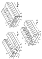
- a layer of insulating material 10 preferably silicon dioxide, is mounted or deposited on a base layer 12.
- the deposit is preferably by chemical vapor deposition (CVD).
- CVD chemical vapor deposition
- One preferred technique is performed in a parallel plate reactor using 2% silane (SiH4) with a carrier of He, with an N2O flow of .75 liters/min. at a pressure of 252.7 Pa (1.9 Torr) at 300°C, the upper electrode being biased.
- the base layer preferably is a silicon substrate which has an etch stop 13 such as Al2O3 coated thereon, by conventional methods such as reactive sputtering.
- a layer of photoresist material 14 is applied on to the insulating layer 10. Any conventional photoresist material may be used; and, by conventional photolithographic techniques, the photoresist material 14 is exposed and developed to reveal the underlying substrate 10 in the pattern as shown in Figure 1b.
- the structure is then etched to remove the exposed silicon dioxide in the layer 10, the remaining photoresist material acting as an etch mask.
- the etching is preferably done by reactive ion etching techniques in CHF3 + CO2 or CF4 at a 13.3 Pa (100 Millitorr) or less. The etching continues until all the exposed material has been removed down to the stop 13. Following this the remaining photoresist material is removed with the resulting structure being as shown in Figure 1c in which a trough or trench 16 has been etched into the silicon with groves 18 extending orthogonally therefrom.
- a second layer of a second insulating material 20 is blanket deposited over the first insulating layer 10 and the exposed portion of the underlying stop 13 and preferably is planarized. It is essential that the second insulating material be of a different composition or structure from the first insulating material or in some other way differs such that it will react with an etch media which is essentially unreactive or much less reactive to the first insulating material. Expressed another way, the material 20 must have an etch rate in some etch medium which differs from that of the material 10. In the preferred embodiment this second insulating material 20 is silicon nitride Si3N4. A preferred method is utilizing plasma enhanced chemical vapor deposition (PECVD).
- PECVD plasma enhanced chemical vapor deposition
- SiH4 and NH3 Silane and ammonia
- SiH4 and NH3 Silane
- 175 SCCM of Silane and 325 SCCM of NH3 a presence of 266 Pa (2 Torr) and at 375°C, with a power of 175 watts.
- a photoresist material 22 is then applied over the insulating material 20 and exposed and developed to reveal the underlying insulating material in the layer 20 as shown in Figure 1d.
- edge of the remaining photoresist material, which will act as an etch mask, on the left side 24 is coincident with the edge of the insulating material 10 whereas the edge of the remaining photoresist material on the right side is somewhat offset with the edge of the insulating material 10 on its right side where the trough 16 is forming a step 26 as shown in Figure 1e.
- the silicon nitride is etched anisotopically preferably by reactive ion etching in CHF3+CO2 at a low pressure, e.g. 4 Pa (30 Millitorr) or less. This will selectively anisotopically etch the silicon nitride but will be essentially unreactive with the silicon dioxide in the insulating layer 10.
- the resulting structure is as shown in Figure 1e.
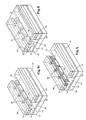
- a third insulating material 28 which must have a different etch rate from that of the insulating material in the second layer and preferably is the same as the insulating material of the first layer, i.e. SiO2 is deposited uniformally over the insulating layers 10 and 20 completely filling the trough 16. It should be noted at this point that the groves 18 in insulating layer 10 are filled with the silicon nitride material of the insulating layer 20.
- a layer of photoresist 30 is applied on top of the third insulating layer 28 and exposed and developed to reveal the underlying silicon dioxide in the insulating layer 28 as shown in Figure 1f. It should be noted that the right side of the remaining photoresist material coincides with the right side of the insulating layer 10 and overhangs the right side of the insulating layer 20 and the left hand side of the exposed photoresist is coincident with the left hand sides of both the insulating layer 10 and the second insulating layer 20. This is shown in Figure 1f.
- the revealed silicon dioxide of the insulating layer 28 is then etched preferably by reactive ion etching techniques as previously described in CHF3 + O2 at 26.6 Pa (200 Millitorr) or less which will result in the structure shown in Figure 1g.
- groves 32 are formed in layer 28 which extend orthagonally with respect to the central trough 16. The remaining photoresist material is then removed.
- the silicon nitride insulating layer 20 is isotopically etched by any conventional technique which will etch the silicon nitride but not the SiO2.
- a preferred technique is to utilize hot phosphoric acid (H3PO4). This will undercut the silicon nitride layer forming a longitudinally extending slot 33 as shown in Figure 1h. This will also remove the silicon nitride in slots 18, also as shown in Figure 1h. It should be noted that this slot 33 is formed only on the left hand side of the structure where the silicon nitride is exposed and not on the right side where the layer 28 of the silicon dioxide covers the edge of the silicon nitride in the insulating layer 20.
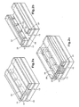
- a layer of metal 34 is conformably deposited as shown in Figure 1i.
- this metal is tungsten which is blanket deposited by conventional CVD techniques.
- a preferred method of blanket depositing the tungsten is to first deposit a seed layer about 50 ⁇ m (500 angstroms) thick of tungsten silicide (WSi2) in a chemical vapor deposition process utilizing WF6 H2 and SiH4 gasses at a pressure of about 20 Pa (150 Millitorr) and a temperature of about 450°C.
- a tungsten metal is deposited also utilizing CVD techniques in WF6 H2 and SiH4 gasses at about 20 Pa (150 Millitorr) and 450°C. These depositions can take place in a coldwall reactor, such technique for deposition of tungsten being well known in the art.
- the tungsten is subjected to a wet chemical etch of dilute peroxides which stops on the seed layer of WSi2.
- the seed layer is etched in a 20/1 ratio of nitric acid and ammonium fluoride. This etch will not etch tungsten or oxides.
- These combined etches will remove the tungsten and WSi2 on the exposed edges of the stack of insulating layers 10 and 28, and the etching is stopped when only the tungsten and WSi2 which is deposited in the slot 33 and in the groves 18 and 32 still remains.
- the basic wiring plan is established and the structure so formed can be utilized for various wiring schemes on various devices.
- this technique is particularly useful if one wishes to have sidewall formed semiconductor devices, since it provides a very viable and well designed technique for connecting to sidewall formed devices.
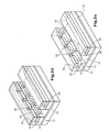
- the photoresist 22 is applied in a band or strip about one micron wide or whatever size is desired for the final electrical line width as shown in Figure 2a.
- the exposed silicon nitride to the left of the photoresist 22 is also removed as well as that in the trough 16 leaving a silicon nitride band 20 of about 1 micron in width below the photoresist 22 as shown in Figure 2b.
- the photoresist 22 is removed, and the silicon dioxide 28 is deposited as previously described, and the photoresist 30 is applied thereon and patterned as previously described, as shown in Figures 2c, and the SiO2 28 etched to form the structure shown in Figure 2d.
- the layer of silicon dioxide 28 also fills in to the left of the silicon nitride layer 20; thus, when the hot phosphoric acid isotopically etches the silicon nitride 20 to produce the structure shown in Figure 2e, the etching will automatically be stopped when all of the silicon nitride has been etched to reveal the layer of silicon dioxide 28 adjacent the silicon nitride.
- the metal can then be deposited and etched in the same manner as described in the previous embodiment and shown in Figures 1i and 1j.
Landscapes
- Internal Circuitry In Semiconductor Integrated Circuit Devices (AREA)
- Printing Elements For Providing Electric Connections Between Printed Circuits (AREA)
- Manufacturing Of Printed Wiring (AREA)
Applications Claiming Priority (2)
| Application Number | Priority Date | Filing Date | Title |
|---|---|---|---|
| US07/285,186 US4985990A (en) | 1988-12-14 | 1988-12-14 | Method of forming conductors within an insulating substrate |
| US285186 | 2002-10-31 |
Publications (3)
| Publication Number | Publication Date |
|---|---|
| EP0373344A2 true EP0373344A2 (de) | 1990-06-20 |
| EP0373344A3 EP0373344A3 (de) | 1991-04-24 |
| EP0373344B1 EP0373344B1 (de) | 1994-08-24 |
Family
ID=23093134
Family Applications (1)
| Application Number | Title | Priority Date | Filing Date |
|---|---|---|---|
| EP89120347A Expired - Lifetime EP0373344B1 (de) | 1988-12-14 | 1989-11-03 | Verfahren zum Herstellen von Leiterbahnen innerhalb eines isolierenden Substrates Isolierendensubstrat |
Country Status (4)
| Country | Link |
|---|---|
| US (1) | US4985990A (de) |
| EP (1) | EP0373344B1 (de) |
| JP (1) | JPH0682757B2 (de) |
| DE (1) | DE68917695T2 (de) |
Cited By (1)
| Publication number | Priority date | Publication date | Assignee | Title |
|---|---|---|---|---|
| EP0587401A3 (en) * | 1992-09-11 | 1996-03-06 | Inmos Ltd | Manufacture of a plug or a via in a semiconductor device |
Families Citing this family (13)
| Publication number | Priority date | Publication date | Assignee | Title |
|---|---|---|---|---|
| US5282071A (en) * | 1992-07-13 | 1994-01-25 | Motorola, Inc. | Contact areas on an optical waveguide and method of making |
| JPH08501663A (ja) * | 1993-07-07 | 1996-02-20 | ダイコネックス パテンテ アクチエンゲゼルシャフト | 構造化プリント回路基板および箔プリント回路基板、およびそれらの製造方法 |
| US5733175A (en) | 1994-04-25 | 1998-03-31 | Leach; Michael A. | Polishing a workpiece using equal velocity at all points overlapping a polisher |
| US5607341A (en) | 1994-08-08 | 1997-03-04 | Leach; Michael A. | Method and structure for polishing a wafer during manufacture of integrated circuits |
| US5814238A (en) * | 1995-10-12 | 1998-09-29 | Sandia Corporation | Method for dry etching of transition metals |
| US6576848B1 (en) | 1996-11-22 | 2003-06-10 | International Business Machines Corporation | Integrated circuit chip wiring structure with crossover capability and method of manufacturing the same |
| US5818110A (en) * | 1996-11-22 | 1998-10-06 | International Business Machines Corporation | Integrated circuit chip wiring structure with crossover capability and method of manufacturing the same |
| US5965465A (en) * | 1997-09-18 | 1999-10-12 | International Business Machines Corporation | Etching of silicon nitride |
| US6150282A (en) * | 1997-11-13 | 2000-11-21 | International Business Machines Corporation | Selective removal of etching residues |
| US6033996A (en) * | 1997-11-13 | 2000-03-07 | International Business Machines Corporation | Process for removing etching residues, etching mask and silicon nitride and/or silicon dioxide |
| US6117796A (en) * | 1998-08-13 | 2000-09-12 | International Business Machines Corporation | Removal of silicon oxide |
| US6200891B1 (en) | 1998-08-13 | 2001-03-13 | International Business Machines Corporation | Removal of dielectric oxides |
| US7758350B2 (en) * | 2007-04-26 | 2010-07-20 | Teka Interconnection Systems | Electrical connector with solder retention means for assembly |
Family Cites Families (12)
| Publication number | Priority date | Publication date | Assignee | Title |
|---|---|---|---|---|
| US3151278A (en) * | 1960-08-22 | 1964-09-29 | Amphenol Borg Electronics Corp | Electronic circuit module with weldable terminals |
| US3372474A (en) * | 1963-11-08 | 1968-03-12 | Sanders Associates Inc | System for weldable circuits |
| US3629939A (en) * | 1969-02-10 | 1971-12-28 | Sanders Associates Inc | Multilayer core memory process |
| FR2204940B1 (de) * | 1972-10-27 | 1976-01-30 | Thomson Csf Fr | |
| US4415403A (en) * | 1978-11-20 | 1983-11-15 | Dynamics Research Corporation | Method of fabricating an electrostatic print head |
| JPS5595340A (en) * | 1979-01-10 | 1980-07-19 | Chiyou Lsi Gijutsu Kenkyu Kumiai | Preparation of semiconductor device |
| US4213807A (en) * | 1979-04-20 | 1980-07-22 | Rca Corporation | Method of fabricating semiconductor devices |
| US4334348A (en) * | 1980-07-21 | 1982-06-15 | Data General Corporation | Retro-etch process for forming gate electrodes of MOS integrated circuits |
| US4520561A (en) * | 1983-12-16 | 1985-06-04 | Rca Corporation | Method of fabricating an electronic circuit including an aperture through the substrate thereof |
| JPH07118474B2 (ja) * | 1984-12-17 | 1995-12-18 | ソニー株式会社 | エツチングガス及びこれを用いたエツチング方法 |
| US4642665A (en) * | 1984-12-19 | 1987-02-10 | Eaton Corporation | Vertically layered MOMOM tunnel device |
| US4663831A (en) * | 1985-10-08 | 1987-05-12 | Motorola, Inc. | Method of forming transistors with poly-sidewall contacts utilizing deposition of polycrystalline and insulating layers combined with selective etching and oxidation of said layers |
-
1988
- 1988-12-14 US US07/285,186 patent/US4985990A/en not_active Expired - Fee Related
-
1989
- 1989-11-03 DE DE68917695T patent/DE68917695T2/de not_active Expired - Fee Related
- 1989-11-03 EP EP89120347A patent/EP0373344B1/de not_active Expired - Lifetime
- 1989-12-14 JP JP1322775A patent/JPH0682757B2/ja not_active Expired - Lifetime
Non-Patent Citations (1)
| Title |
|---|
| IBM TECHNICAL DISCLOSURE BULLETIN. vol. 31, no. 4, September 1988, NEW YORK US pages 400 - 401; "SINGLE-STEP, MULTILEVEL, METALLISATION TECHNIQUE FOR COFORMAL WIRING" * |
Cited By (2)
| Publication number | Priority date | Publication date | Assignee | Title |
|---|---|---|---|---|
| EP0587401A3 (en) * | 1992-09-11 | 1996-03-06 | Inmos Ltd | Manufacture of a plug or a via in a semiconductor device |
| US5874360A (en) * | 1992-09-11 | 1999-02-23 | Sgs-Thomson Microelectronics Limited | Manufacture of semiconductor devices |
Also Published As
| Publication number | Publication date |
|---|---|
| DE68917695T2 (de) | 1995-03-30 |
| EP0373344A3 (de) | 1991-04-24 |
| JPH0682757B2 (ja) | 1994-10-19 |
| US4985990A (en) | 1991-01-22 |
| EP0373344B1 (de) | 1994-08-24 |
| JPH02230757A (ja) | 1990-09-13 |
| DE68917695D1 (de) | 1994-09-29 |
Similar Documents
| Publication | Publication Date | Title |
|---|---|---|
| EP0373344B1 (de) | Verfahren zum Herstellen von Leiterbahnen innerhalb eines isolierenden Substrates Isolierendensubstrat | |
| KR100337580B1 (ko) | 반도체장치및그제조방법 | |
| US5686354A (en) | Dual damascene with a protective mask for via etching | |
| US6617245B2 (en) | Etching mask, process for forming contact holes using same, and semiconductor device made by the process | |
| US4634496A (en) | Method for planarizing the surface of an interlayer insulating film in a semiconductor device | |
| US4946550A (en) | Forming electrical connections for electronic devices | |
| US4818334A (en) | Method of etching a layer including polysilicon | |
| EP0545263A2 (de) | Verfahren zur Herstellung einer Isolationsprobe mittels einer Polierschritt | |
| US6323118B1 (en) | Borderless dual damascene contact | |
| US5312773A (en) | Method of forming multilayer interconnection structure | |
| US5665657A (en) | Spin-on-glass partial etchback planarization process | |
| US5025303A (en) | Product of pillar alignment and formation process | |
| US5227191A (en) | Method of forming multilayer interconnection structure | |
| EP0424485B1 (de) | Vollverdiefte verbindungsstruktur mit titanium/wolfram und selektivem cvd-wolfram | |
| KR20000029433A (ko) | 반도체 기억장치의 제조방법 | |
| US5136124A (en) | Method of forming conductors within an insulating substrate | |
| US4755482A (en) | Making semiconductor device on insulating substrate by forming conductive layers on both major surfaces | |
| US5128278A (en) | Method of forming a wiring pattern for a semiconductor device | |
| EP0324198B1 (de) | Verfahren zum Herstellen von elektrischen Kontakten in integrierten Schaltungen | |
| JP3317279B2 (ja) | 半導体装置の製造方法 | |
| JP3080055B2 (ja) | ドライエッチング方法 | |
| US5756397A (en) | Method of fabricating a wiring in a semiconductor device | |
| JPS63117447A (ja) | 半導体集積回路の製造方法 | |
| JPH0422021B2 (de) | ||
| US5612572A (en) | Semiconductor device with an insulation groove |
Legal Events
| Date | Code | Title | Description |
|---|---|---|---|
| PUAI | Public reference made under article 153(3) epc to a published international application that has entered the european phase |
Free format text: ORIGINAL CODE: 0009012 |
|
| AK | Designated contracting states |
Kind code of ref document: A2 Designated state(s): DE FR GB |
|
| 17P | Request for examination filed |
Effective date: 19901025 |
|
| PUAL | Search report despatched |
Free format text: ORIGINAL CODE: 0009013 |
|
| AK | Designated contracting states |
Kind code of ref document: A3 Designated state(s): DE FR GB |
|
| 17Q | First examination report despatched |
Effective date: 19931104 |
|
| GRAA | (expected) grant |
Free format text: ORIGINAL CODE: 0009210 |
|
| AK | Designated contracting states |
Kind code of ref document: B1 Designated state(s): DE FR GB |
|
| REF | Corresponds to: |
Ref document number: 68917695 Country of ref document: DE Date of ref document: 19940929 |
|
| ET | Fr: translation filed | ||
| PLBE | No opposition filed within time limit |
Free format text: ORIGINAL CODE: 0009261 |
|
| STAA | Information on the status of an ep patent application or granted ep patent |
Free format text: STATUS: NO OPPOSITION FILED WITHIN TIME LIMIT |
|
| 26N | No opposition filed | ||
| PGFP | Annual fee paid to national office [announced via postgrant information from national office to epo] |
Ref country code: DE Payment date: 19951123 Year of fee payment: 7 |
|
| PGFP | Annual fee paid to national office [announced via postgrant information from national office to epo] |
Ref country code: FR Payment date: 19961112 Year of fee payment: 8 |
|
| PG25 | Lapsed in a contracting state [announced via postgrant information from national office to epo] |
Ref country code: DE Effective date: 19970801 |
|
| PG25 | Lapsed in a contracting state [announced via postgrant information from national office to epo] |
Ref country code: FR Free format text: THE PATENT HAS BEEN ANNULLED BY A DECISION OF A NATIONAL AUTHORITY Effective date: 19971130 |
|
| REG | Reference to a national code |
Ref country code: FR Ref legal event code: ST |
|
| PGFP | Annual fee paid to national office [announced via postgrant information from national office to epo] |
Ref country code: GB Payment date: 19981027 Year of fee payment: 10 |
|
| PG25 | Lapsed in a contracting state [announced via postgrant information from national office to epo] |
Ref country code: GB Free format text: LAPSE BECAUSE OF NON-PAYMENT OF DUE FEES Effective date: 19991103 |
|
| GBPC | Gb: european patent ceased through non-payment of renewal fee |
Effective date: 19991103 |