EP0375232B1 - Thermisches Oxydierungsverfahren mit verändertem Wachstum für dünne Oxide - Google Patents
Thermisches Oxydierungsverfahren mit verändertem Wachstum für dünne Oxide Download PDFInfo
- Publication number
- EP0375232B1 EP0375232B1 EP89312879A EP89312879A EP0375232B1 EP 0375232 B1 EP0375232 B1 EP 0375232B1 EP 89312879 A EP89312879 A EP 89312879A EP 89312879 A EP89312879 A EP 89312879A EP 0375232 B1 EP0375232 B1 EP 0375232B1
- Authority
- EP
- European Patent Office
- Prior art keywords
- oxide
- growth
- silicon surface
- silicon
- preoxidation
- Prior art date
- Legal status (The legal status is an assumption and is not a legal conclusion. Google has not performed a legal analysis and makes no representation as to the accuracy of the status listed.)
- Expired - Lifetime
Links
Images


Classifications
-
- H—ELECTRICITY
- H10—SEMICONDUCTOR DEVICES; ELECTRIC SOLID-STATE DEVICES NOT OTHERWISE PROVIDED FOR
- H10P—GENERIC PROCESSES OR APPARATUS FOR THE MANUFACTURE OR TREATMENT OF DEVICES COVERED BY CLASS H10
- H10P14/00—Formation of materials, e.g. in the shape of layers or pillars
- H10P14/60—Formation of materials, e.g. in the shape of layers or pillars of insulating materials
- H10P14/65—Formation of materials, e.g. in the shape of layers or pillars of insulating materials characterised by treatments performed before or after the formation of the materials
- H10P14/6502—Formation of materials, e.g. in the shape of layers or pillars of insulating materials characterised by treatments performed before or after the formation of the materials of treatments performed before formation of the materials
- H10P14/6504—In-situ cleaning
-
- H—ELECTRICITY
- H10—SEMICONDUCTOR DEVICES; ELECTRIC SOLID-STATE DEVICES NOT OTHERWISE PROVIDED FOR
- H10P—GENERIC PROCESSES OR APPARATUS FOR THE MANUFACTURE OR TREATMENT OF DEVICES COVERED BY CLASS H10
- H10P14/00—Formation of materials, e.g. in the shape of layers or pillars
- H10P14/60—Formation of materials, e.g. in the shape of layers or pillars of insulating materials
- H10P14/65—Formation of materials, e.g. in the shape of layers or pillars of insulating materials characterised by treatments performed before or after the formation of the materials
- H10P14/6502—Formation of materials, e.g. in the shape of layers or pillars of insulating materials characterised by treatments performed before or after the formation of the materials of treatments performed before formation of the materials
- H10P14/6512—Formation of materials, e.g. in the shape of layers or pillars of insulating materials characterised by treatments performed before or after the formation of the materials of treatments performed before formation of the materials by exposure to a gas or vapour
-
- H—ELECTRICITY
- H10—SEMICONDUCTOR DEVICES; ELECTRIC SOLID-STATE DEVICES NOT OTHERWISE PROVIDED FOR
- H10P—GENERIC PROCESSES OR APPARATUS FOR THE MANUFACTURE OR TREATMENT OF DEVICES COVERED BY CLASS H10
- H10P14/00—Formation of materials, e.g. in the shape of layers or pillars
- H10P14/60—Formation of materials, e.g. in the shape of layers or pillars of insulating materials
- H10P14/63—Formation of materials, e.g. in the shape of layers or pillars of insulating materials characterised by the formation processes
- H10P14/6302—Non-deposition formation processes
- H10P14/6304—Formation by oxidation, e.g. oxidation of the substrate
- H10P14/6306—Formation by oxidation, e.g. oxidation of the substrate of the semiconductor materials
- H10P14/6308—Formation by oxidation, e.g. oxidation of the substrate of the semiconductor materials of Group IV semiconductors
- H10P14/6309—Formation by oxidation, e.g. oxidation of the substrate of the semiconductor materials of Group IV semiconductors of silicon in uncombined form, i.e. pure silicon
-
- H—ELECTRICITY
- H10—SEMICONDUCTOR DEVICES; ELECTRIC SOLID-STATE DEVICES NOT OTHERWISE PROVIDED FOR
- H10P—GENERIC PROCESSES OR APPARATUS FOR THE MANUFACTURE OR TREATMENT OF DEVICES COVERED BY CLASS H10
- H10P14/00—Formation of materials, e.g. in the shape of layers or pillars
- H10P14/60—Formation of materials, e.g. in the shape of layers or pillars of insulating materials
- H10P14/63—Formation of materials, e.g. in the shape of layers or pillars of insulating materials characterised by the formation processes
- H10P14/6302—Non-deposition formation processes
- H10P14/6322—Formation by thermal treatments
-
- Y—GENERAL TAGGING OF NEW TECHNOLOGICAL DEVELOPMENTS; GENERAL TAGGING OF CROSS-SECTIONAL TECHNOLOGIES SPANNING OVER SEVERAL SECTIONS OF THE IPC; TECHNICAL SUBJECTS COVERED BY FORMER USPC CROSS-REFERENCE ART COLLECTIONS [XRACs] AND DIGESTS
- Y10—TECHNICAL SUBJECTS COVERED BY FORMER USPC
- Y10S—TECHNICAL SUBJECTS COVERED BY FORMER USPC CROSS-REFERENCE ART COLLECTIONS [XRACs] AND DIGESTS
- Y10S148/00—Metal treatment
- Y10S148/118—Oxide films
-
- Y—GENERAL TAGGING OF NEW TECHNOLOGICAL DEVELOPMENTS; GENERAL TAGGING OF CROSS-SECTIONAL TECHNOLOGIES SPANNING OVER SEVERAL SECTIONS OF THE IPC; TECHNICAL SUBJECTS COVERED BY FORMER USPC CROSS-REFERENCE ART COLLECTIONS [XRACs] AND DIGESTS
- Y10—TECHNICAL SUBJECTS COVERED BY FORMER USPC
- Y10S—TECHNICAL SUBJECTS COVERED BY FORMER USPC CROSS-REFERENCE ART COLLECTIONS [XRACs] AND DIGESTS
- Y10S438/00—Semiconductor device manufacturing: process
- Y10S438/974—Substrate surface preparation
Definitions
- the present invention relates to a growth-modified thermal oxidation process for forming thin (e.g., ⁇ 25 nm) oxides for use in silicon integrated circuits.
- the Kern et al. article discusses the use of various solutions, including H2O2-NH4OH and H2-H2O2-HCl to prepare a silicon surface for oxidation.
- This preoxidation cleaning has become an integral part of oxidation technology.
- Such cleaning processes cannot alleviate the problems of growth-induced oxide defects and interfacial stress between the silicon substrate and the grown oxide.
- a small amount of a chlorine-bearing vapor may be added to the oxidant during growth.
- This particular work is described in detail in the reference entitled "The Use of 1.1.1-Trichloroethane as an Optimized Additive to Improve the Silicon Thermal Oxidation Technology", by E.J. Janssens et al. appearing in the Journal Electrochem. Society , Vol. 125, No. 10, October 1978, pp. 1696-1703.
- the addition of the chlorine-bearing species for example, hydrochloric acid (HCl), trichloroethane (TCA), trichloroethene (TCE)
- HCl hydrochloric acid
- TCA trichloroethane
- TCE trichloroethene
- D o 0.5cm ⁇
- the Si3N4/SiO2 interface is known to exhibit a high density of interface charge trapping states, Q it , which cannot be removed by annealing since the nitride is impervious to the oxidizing species.
- This tri-level structure is unsuitable as a gate dielectric in MOS integrated circuits, as these interface states may cause charge-induced shifts in threshold voltage, as well as a reduction in channel conductance during device operation.
- the present invention relates to a growth-modified thermal oxidation process for forming thin (e.g., ⁇ 25nm) oxides and, more particularly, to a process including in situ preoxidation silicon surface treatments which result in minimizing growth abnormalities in the growing oxide layer, thus improving the quality of the oxide structure and the substrate/oxide interface.
- an in situ Cl ⁇ for example, HCl, HCA or TCE
- a high-temperature ( ⁇ 900-950°C) stress-relief anneal are utilised.
- the growth-modified oxidation process of the present invention relates to the formation of a thermally grown oxide layer.
- Thermal oxidation of silicon occurs by Fickian diffusion of the oxidant through the grown oxide and the reaction of the oxidant with the silicon at the Si/SiO2 interface by a first-order chemical process. The process results in an inward propagation of this interface and generates the best possible passivation for the silicon layer.
- Other types of processes for example, chemical vapor deposition (CVD), results in relatively inferior passivation where the deposited oxide layer exhibits a relatively poor quality dielectric for gate oxide applications in ultra-large scale integration (ULSI) of semiconductor integrated circuits.
- ULSI ultra-large scale integration
- FIG. 1 outlines the processing sequence for both a prior art thermal oxidation process and an exemplary growth-modified process of this invention.
- the silicon wafer is transferred into the furnace during the time period t′1-t′2 (10 minutes, typical).
- the furnace temperature during this initial period, T i ′ is approximately 750°C.
- the temperature of the furnace is ramped up to its final value, T f ′, of approximately 900°C.
- a typical ramping of 5°C/min may be used, requiring approximately 40 minutes to bring the furnace to temperature T f ′.
- the wafers are then exposed to an oxygen ambient to begin the formation of the oxide layer.
- a chlorine-bearing species may be included with this oxygen ambient to further improve the qualiry of the growing oxide layer.
- the oxygen exposure proceeds for the time period t′3-t′4, where the length of this period depends on the desired thickness of the oxide layer. For example, a 20-30 minute exposure will grow an oxide approximately 250 nm thick.
- a post-oxidation anneal from t4′ to t5′ is then performed to eliminate any trapped charges from the grown oxide film.
- the temperature of the furnace is then slowly ramped down to its initial value of T i ′ during time period t5′-t6′.
- the wafer is then slowly removed from the furnace during time period t6′-t7′.
- the stress results for the 25 nm layer are illustrated in graph form in FIG. 2 and will be discussed in detail hereinafter with respect to FIG. 2.
- the growth-modified oxidation process of the present invention has been found to improve these and other characteristics of a thermally grown thin oxide.
- One exemplary process sequence is illustrated in FIG. 1, where it may be easily compared against the prior art process described above.
- the process begins with the transport of the wafer into the furnace during t1-t2 (10 minutes), similar to the prior art process.
- the initial temperature, T i of the furnace at this point is approximately 750° C.
- a first surface treatment occurs, a gettering of the silicon surface in a dilute chlorine containing ambient (for example, HCl or TCA or TCE).
- the gettering during time period t2-t3 (thirty minutes, for example) is utilized to remove any metal-ion contaminants which may exist on the silicon nucleation surface.
- the concentration of mobile ions, N mi will be significantly reduced in the grown oxide, when compared with prior art structures.
- the temperature of the furnace is ramped up during time period t3-t4 to the T f of 900°C (the same 5°C/min ramp procedure may be used).
- a second surface treatment, a stress-relief anneal, is introduced at this point during time period t4-t5.
- An anneal in an inert atmosphere (100% Ar, for example) is performed (approximately thirty minutes) to minimize the local variations in the stress fields near the silicon surface.
- the stress at the silicon surface is the result of a small amount of native oxide which begins to form on the nucleation surface even before the actual oxidation step is initiated.
- the native oxide, being discontinuous will always generate local stress gradients in silicon due to thermal expansion mismatch of Si and Si02, and also due to the large change in index volume associated with the Si ⁇ Si02 transformation. These locally stressed regions affect the oxidation growth kinetics and the Si/Si02 interface substructure.
- the effect of these local stress gradients on the quality of the grown oxide becomes further amplified due to complex processing and device geometries.
- the argon anneal is thought to relax at least some of these locally stressed zones and thereby reduce some of the growth abnormalities in the grown oxide layer.
- the procedure may be identical to the prior art sequence described above.
- the oxidation of the silicon surface occurs during time period t5-t6 (where again, the length of time is related to the desired thickness of the oxide), followed by an anneal during time period t6-t7.
- the temperature of the furnace is then ramped down during time period t7-t8 and the oxidized wafer removed from the furnace.
- the silicon stress data are illustrated in graph form in FIG. 2. A comparison of these results with those of the prior art thermal oxide illustrates the significant improvement in thin oxide quality when the preoxidation silicon surface treatments of the present invention are utilized.
- Table 1 summarizes these various properties discussed above for four different oxides: (1) a prior art thermal oxide; (2) a growth-modified oxide grown using both a preoxidation contamination getter and a preoxidation stress-relief anneal; (3) a growth-modified oxide grown using only a preoxidation contamination getter; and (4) a growth-modified oxide grown using only a preoxidation stress-relief anneal.
- a growth-modified process including both a gettering operation and an anneal is the preferred alternative in achieving the best quality thin oxide.
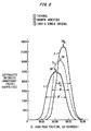
- FIG. 2 contains plots of the silicon (400) X-ray microdiffraction (XRMD) peak profiles for the following: (1) a structure containing a prior art thermal oxide; (2) a structure containing a growth-modified oxide; and (3) a nominal silicon substrate without any oxide, the latter being included for comparison purposes only.
- XRMD X-ray microdiffraction
- any deviation in peak position from the unstressed value of 2 ⁇ o is a measure of lattice dilation (d-d o or ⁇ d ) that can be converted to the stress in silicon ( ⁇ si ) from the known elastic stiffness values of silicon.
- the peak breadth, denoted ⁇ , of the silicon (400) peak profile provides information about the silicon substructure the silicon near the Si/SiO2 interface.
- the peak profile for nominal (100) single crystal silicon is seen to be relatively narrow, with a 2 ⁇ o peak position of 69.1975° and a width ⁇ o of approximately 0.7000°.
- the peak profile for the structure with a prior art thermal oxide is seen to be much broader, with a ⁇ ′ of approximately 0.7300°.
- this broadening is related to an increase in the silicon defect density near the interface.
- the 2 ⁇ ′ peak position is seen to have shifted to a value of 69.1400°, indicating an increase in stress in a structure which includes a prior art thermal oxide.
- the peak profile associated with the growth-modified structure of the present invention is seen to provide improvement in both peak position 2 ⁇ and peak width ⁇ .
- a preoxidation silicon surface treatment in the form of an in situ getter has been found to remove metal-ion contaminants from the silicon nucleation surface, thus reducing growth anomalies in the oxide layer and lowering the defect density.
- the gettering operation will provide a shift in the 2 ⁇ peak position closer towards the nominal value associated with (100) single crystal silicon. In this case, as seen by reference to FIG. 2, a value for 2 ⁇ of 69.1820° was achieved.
- the narrowing of the peak width, ⁇ is provided by relieving the stress in the silicon substrate near the interface with the oxide.
- Stress relief is accomplished by a preoxidation silicon surface treatment in the form of a high temperature anneal. As illustrated in FIG. 2, such a process has been found to shrink the peak width ⁇ to a value of approximately 0.7180°, relatively close to the nominal width of 0.7000°, associated with the (100) single crystal silicon substrate.
- FIG. 3 contains lattice images obtained with transmission electron microscopy (TEM) of both a structure with a prior art thermal oxide (left-hand image) and a structure with a growth-modified oxide formed in accordance with the present invention (right-hand image).
- the relatively large contrast modulation (as indicated by the darker areas) in the lattice image of the silicon layer near the interface in the prior art thermal oxide is attributed to localized strain fields.
- Such strain fields in the silicon layer are substantially reduced in the structure formed with the growth-modified process of the present invention when a preoxidation stress relief anneal is employed prior to the initiation of the thermal oxide growth.
- This strain reduction is represented in the lattice image of the growth-modified oxide by the uniformity of the structure, especially noticeable at the substrate/oxide interface. Additionally, an in situ preoxidation getter for removing contaminants has been found to further reduce this contrast modulation.
- the improvements made by the preoxidation silicon surface treatments of the present invention are cumulative. It is to be noted, also, that the order in which these operations are performed is not critical. That is, a stress-relief anneal may be performed prior to a contaminant getter (indeed, a gettering operation may be performed at T f of 900°C). However, since the annealing must be performed at an elevated temperature, the process as outlined in FIG. 1 is considered to be the most logical sequence for incorporating these preoxidation silicon surface treatments into a standard manufacturing process.
- the oxidation may also be performed by a rapid thermal oxidation (RTO) process using lasers, electron beams, or incoherent halogen lamps as a heating source for very short, high temperature treatments to control this thermally-driven surface reaction.
- RTO rapid thermal oxidation
- the transport of the oxidant through the growing oxide layer is normally driven by thermal energy, the oxidation may be performed at a relatively low temperature in an environment enhanced by a photon flux or an electric field, where these conditions are known to provide transport of the oxidizing species to the substrate interface and allow oxidation to take place.
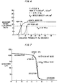
- An exemplary method which was used to measure the defect density D o of a growth-modified thin oxide formed in accordance with the present invention required the utilization of an actual device structure (for example, a 1 Mbit DRAM), processed through the steps of local oxidation, polysilicon deposition and doping so as to form a capacitor structure.
- the device was then patterned to form a single field plate over the entire chip, as illustrated in FIG. 4.
- Tests were performed by applying a negative voltage ramp to the field plate (-1V/sec at the applied bias, for example) until a leakage current level of 1 ⁇ A was reached.
- a schematic diagram of the test structure is illustrated in FIG. 5.
- the data for both a prior art thermal oxide and a growth-modified oxide of the present invention are illustrated in FIG. 6.
- the yield Y increased from approximately 82% for the prior art thermal oxide to approximately 96% for the growth-modified oxide of the present invention.
- the defect density D o decreased from a value of 0.7000 ⁇ for the prior art thermal oxide to a level of approximately 0.2cm ⁇ for the growth-modified oxide.
- the improvement in both yield and D o for the growth-modified oxide films are apparent.
- C-V capacitance-voltage
- BTS bias-temperature-stressing
- ⁇ V FB flat band voltage shift
- the C-V characteristics for MOS capacitors including a growth-modified oxide film are illustrated in FIG. 8.
- ⁇ V FB -0.03V
- FIG. 6(a) These results indicate lower trapped charge (Q it ), flat band shift ( ⁇ V FB ) and mobile ion concentration (N mi ) in growth-modified films when compared to prior art thermal oxide films of an equivalent thickness.
- FIGs. 9-11 illustrate the combined high and low frequency C-V plots for three different oxides: (a) a stacked oxide comprising a prior art SiO2/Si3N4 structure (FIG. 9); (b) a prior art thermal oxide structure (FIG. 10); and (c) a growth-modified oxide of the present invention (FIG. 11).
- the large difference in capacitance, denoted by the letter "A”, at the onset of inversion for the stacked oxide plots of FIG. 9 is attributed to the high density of interface traps Q it at the interface between the SiO2 and Si3N4 layers. These traps also account for the modulation present in the inversion region of the low frequency plot.
- the growth-modified oxide as seen by reference to FIG. 11 illustrates a slight improvement in the low frequency inversion region, in terms of linearity of capacitance, when compared to the prior art thermal oxide plot of FIG. 10.
Landscapes
- Formation Of Insulating Films (AREA)
- Insulated Gate Type Field-Effect Transistor (AREA)
- Silicon Compounds (AREA)
Claims (3)
- Verfahren zur Herstellung einer Halbleiteranordnung mit einer relativ dünnen thermischen Oxidschicht, die an einer Siliciumoberfläche aufgewachsen ist, wobei das Verfahren eine In-Situ-Siliciumoberflächen-Voroxidationsbehandlung vor dem Anfang des Oxidwachstums umfaßt, wobei die Voroxidationsbehandlung und das Oxidwachstum die Schritte umfassen:a) des Bereitstellens einer Siliciumoberfläche bei einer ersten Umgebungstemperatur in dem Bereich von 600°C bis 750°C und gettern der Siliciumoberfläche bei dieser Tempertur in einer verdünnten Chlor enthaltenden Umgebung, um Kontaminationen an dieser Siliciumoberfläche zu entfernen, undb) das Erhöhen der Umgebungstemperatur auf einen zweiten Wert, der für die Oxidation in dem Bereich von 900°C bis 950°C benötigt wird und Annealen der Siliciumoberfläche, die in Schritt a) gegettert wurde, in einer inerten Atmosphäre, wobei das Annealen durchgeführt wird, um lokale Spannungsänderungen in der Siliciumoberfläche zu minimieren, gefolgt vonc) dem Beginnen und Aufrechterhalten des Oxidwachstums durch Aussetzen der Siliciumoberfläche einer Sauerstoffumgebung während einer Zeitdauer, die von der erwünschten Dicke des aufgewachsenen Oxids abhängt, undd) Entfernen der Sauerstoffumgebung, um das Oxidwachstum zu beenden, und wobei die Reihenfolge der Voroxidationsbehandlungsschritte (a) und (b) umgekehrt werden kann.
- Verfahren nach Anspruch 1, bei welchem bei Durchführen des Voroxidationsschrittes (a) die Chlor enthaltende Umgebung ausgewählt ist aus der Gruppe, die Chlorwasserstoffsäure, Trichloroethan und Trichloroethen umfaßt.
- Verfahren nach Anspruch 1, bei welchem beim Durchführen des Voroxidationsschrittes (b) eine Argonumgebung verwendet wird.
Applications Claiming Priority (2)
| Application Number | Priority Date | Filing Date | Title |
|---|---|---|---|
| US28797688A | 1988-12-21 | 1988-12-21 | |
| US287976 | 1988-12-21 |
Publications (3)
| Publication Number | Publication Date |
|---|---|
| EP0375232A2 EP0375232A2 (de) | 1990-06-27 |
| EP0375232A3 EP0375232A3 (en) | 1990-08-22 |
| EP0375232B1 true EP0375232B1 (de) | 1996-03-06 |
Family
ID=23105207
Family Applications (1)
| Application Number | Title | Priority Date | Filing Date |
|---|---|---|---|
| EP89312879A Expired - Lifetime EP0375232B1 (de) | 1988-12-21 | 1989-12-11 | Thermisches Oxydierungsverfahren mit verändertem Wachstum für dünne Oxide |
Country Status (6)
| Country | Link |
|---|---|
| US (1) | US5132244A (de) |
| EP (1) | EP0375232B1 (de) |
| JP (1) | JPH0648683B2 (de) |
| CA (1) | CA2005785A1 (de) |
| DE (1) | DE68925879T2 (de) |
| ES (1) | ES2084606T3 (de) |
Families Citing this family (27)
| Publication number | Priority date | Publication date | Assignee | Title |
|---|---|---|---|---|
| US5354695A (en) | 1992-04-08 | 1994-10-11 | Leedy Glenn J | Membrane dielectric isolation IC fabrication |
| US6714625B1 (en) | 1992-04-08 | 2004-03-30 | Elm Technology Corporation | Lithography device for semiconductor circuit pattern generation |
| US5506178A (en) * | 1992-12-25 | 1996-04-09 | Sony Corporation | Process for forming gate silicon oxide film for MOS transistors |
| JPH0745603A (ja) * | 1993-07-27 | 1995-02-14 | Shin Etsu Handotai Co Ltd | 半導体装置の製造方法及びその製造工程の管理方法 |
| KR100187674B1 (ko) * | 1994-07-07 | 1999-06-01 | 김주용 | 반도체 소자 제조용 반응로 및 그를 이용한 게이트 산화막 형성방법 |
| JP3417665B2 (ja) * | 1994-07-07 | 2003-06-16 | 株式会社東芝 | 半導体装置の製造方法 |
| JP3542189B2 (ja) * | 1995-03-08 | 2004-07-14 | 株式会社ルネサステクノロジ | 半導体装置の製造方法及び半導体装置 |
| US6548854B1 (en) | 1997-12-22 | 2003-04-15 | Agere Systems Inc. | Compound, high-K, gate and capacitor insulator layer |
| JPH10209168A (ja) * | 1997-01-24 | 1998-08-07 | Nec Corp | 半導体装置の製造方法 |
| US6551857B2 (en) | 1997-04-04 | 2003-04-22 | Elm Technology Corporation | Three dimensional structure integrated circuits |
| US5915167A (en) | 1997-04-04 | 1999-06-22 | Elm Technology Corporation | Three dimensional structure memory |
| US5851892A (en) * | 1997-05-07 | 1998-12-22 | Cypress Semiconductor Corp. | Fabrication sequence employing an oxide formed with minimized inducted charge and/or maximized breakdown voltage |
| US6147388A (en) * | 1997-11-24 | 2000-11-14 | Lucent Technologies, Inc. | Polycide gate structure with intermediate barrier |
| US5981403A (en) * | 1997-11-24 | 1999-11-09 | Lucent Technologies, Inc. | Layered silicon nitride deposition process |
| US6271153B1 (en) | 1998-07-22 | 2001-08-07 | Micron Technology, Inc. | Semiconductor processing method and trench isolation method |
| US6177363B1 (en) * | 1998-09-29 | 2001-01-23 | Lucent Technologies Inc. | Method for forming a nitride layer suitable for use in advanced gate dielectric materials |
| US6221790B1 (en) * | 1998-11-19 | 2001-04-24 | Taiwan Semiconductor Manufacturing Company | Stable thin film oxide standard |
| US6748994B2 (en) * | 2001-04-11 | 2004-06-15 | Avery Dennison Corporation | Label applicator, method and label therefor |
| US7144822B1 (en) * | 2002-02-06 | 2006-12-05 | Novellus Systems, Inc. | High density plasma process for optimum film quality and electrical results |
| US7402897B2 (en) | 2002-08-08 | 2008-07-22 | Elm Technology Corporation | Vertical system integration |
| US7084048B2 (en) * | 2004-05-07 | 2006-08-01 | Memc Electronic Materials, Inc. | Process for metallic contamination reduction in silicon wafers |
| RU2344511C1 (ru) * | 2007-04-09 | 2009-01-20 | Государственное образовательное учреждение высшего профессионального образования Кабардино-Балкарский государственный университет им. Х.М. Бербекова | Способ изготовления пленок диоксида кремния |
| JP5996217B2 (ja) * | 2012-03-02 | 2016-09-21 | アルプス電気株式会社 | ガラス複合体、ガラス複合体を用いた入力装置、及び、電子機器 |
| RU2539801C1 (ru) * | 2013-07-01 | 2015-01-27 | Федеральное государственное бюджетное образовательное учреждение высшего профессионального образования "Кабардино-Балкарский государственный университет им. Х.М. Бербекова" (КБГУ) | Способ изготовления тонкого слоя диоксида кремния |
| RU2688864C1 (ru) * | 2018-03-12 | 2019-05-22 | Федеральное государственное бюджетное образовательное учреждение высшего образования "Кабардино-Балкарский государственный университет им. Х.М. Бербекова" (КБГУ) | Способ изготовления полупроводникового прибора |
| RU2688881C1 (ru) * | 2018-04-18 | 2019-05-22 | Федеральное государственное бюджетное образовательное учреждение высшего образования "Кабардино-Балкарский государственный университет им. Х.М. Бербекова" (КБГУ) | Способ изготовления полупроводникового прибора |
| RU2680989C1 (ru) * | 2018-05-07 | 2019-03-01 | Федеральное государственное бюджетное образовательное учреждение высшего образования "Чеченский государственный университет" | Способ изготовления полупроводникового прибора |
Family Cites Families (25)
| Publication number | Priority date | Publication date | Assignee | Title |
|---|---|---|---|---|
| US3447238A (en) * | 1965-08-09 | 1969-06-03 | Raytheon Co | Method of making a field effect transistor by diffusion,coating with an oxide and placing a metal layer on the oxide |
| US3698948A (en) * | 1968-07-26 | 1972-10-17 | Motorola Inc | Fabrication of a silicon-silicon dioxide interface of predetermined space charge polarity |
| US3770498A (en) * | 1971-03-01 | 1973-11-06 | Teledyne Semiconductor | Passivating solution and method |
| US4007297A (en) * | 1971-09-20 | 1977-02-08 | Rca Corporation | Method of treating semiconductor device to improve its electrical characteristics |
| US3800411A (en) * | 1972-05-22 | 1974-04-02 | Litton Systems Inc | Method of forming a stable mnos igfet |
| US3997368A (en) * | 1975-06-24 | 1976-12-14 | Bell Telephone Laboratories, Incorporated | Elimination of stacking faults in silicon devices: a gettering process |
| US4048350A (en) * | 1975-09-19 | 1977-09-13 | International Business Machines Corporation | Semiconductor device having reduced surface leakage and methods of manufacture |
| JPS5297666A (en) * | 1976-02-12 | 1977-08-16 | Hitachi Ltd | Production of semiconductor device containing pn junctions |
| NL7604986A (nl) * | 1976-05-11 | 1977-11-15 | Philips Nv | Werkwijze voor het vervaardigen van een halfgeleider- inrichting, en inrichting vervaardigd door toe- passing van de werkwijze. |
| US4159917A (en) * | 1977-05-27 | 1979-07-03 | Eastman Kodak Company | Method for use in the manufacture of semiconductor devices |
| US4149905A (en) * | 1977-12-27 | 1979-04-17 | Bell Telephone Laboratories, Incorporated | Method of limiting stacking faults in oxidized silicon wafers |
| US4140548A (en) * | 1978-05-19 | 1979-02-20 | Maruman Integrated Circuits Inc. | MOS Semiconductor process utilizing a two-layer oxide forming technique |
| US4231809A (en) * | 1979-05-25 | 1980-11-04 | Bell Telephone Laboratories, Incorporated | Method of removing impurity metals from semiconductor devices |
| DE3206376A1 (de) * | 1982-02-22 | 1983-09-01 | Siemens AG, 1000 Berlin und 8000 München | Verfahren zur herstellung von siliziumoxidschichten |
| US4548654A (en) * | 1983-06-03 | 1985-10-22 | Motorola, Inc. | Surface denuding of silicon wafer |
| US4622082A (en) * | 1984-06-25 | 1986-11-11 | Monsanto Company | Conditioned semiconductor substrates |
| DE3516611A1 (de) * | 1985-05-08 | 1986-11-13 | Siemens AG, 1000 Berlin und 8000 München | Verfahren zum herstellen eines halbleiterschaltkreises |
| US4687682A (en) * | 1986-05-02 | 1987-08-18 | American Telephone And Telegraph Company, At&T Technologies, Inc. | Back sealing of silicon wafers |
| FR2605647B1 (fr) * | 1986-10-27 | 1993-01-29 | Nissim Yves | Procede de depot en phase vapeur par flash thermique d'une couche isolante sur un substrat en materiau iii-v, application a la fabrication d'une structure mis |
| NL8603111A (nl) * | 1986-12-08 | 1988-07-01 | Philips Nv | Werkwijze voor het vervaardigen van een halfgeleiderinrichting waarbij een siliciumplak aan zijn oppervlak wordt voorzien van veldoxidegebieden. |
| US4806202A (en) * | 1987-10-05 | 1989-02-21 | Intel Corporation | Field enhanced tunnel oxide on treated substrates |
| US4851370A (en) * | 1987-12-28 | 1989-07-25 | American Telephone And Telegraph Company, At&T Bell Laboratories | Fabricating a semiconductor device with low defect density oxide |
| US4851358A (en) * | 1988-02-11 | 1989-07-25 | Dns Electronic Materials, Inc. | Semiconductor wafer fabrication with improved control of internal gettering sites using rapid thermal annealing |
| US4920076A (en) * | 1988-04-15 | 1990-04-24 | The United States Of America As Represented By The United States Department Of Energy | Method for enhancing growth of SiO2 in Si by the implantation of germanium |
| US4894353A (en) * | 1988-04-29 | 1990-01-16 | Advanced Micro Devices, Inc. | Method of fabricating passivated tunnel oxide |
-
1989
- 1989-12-11 EP EP89312879A patent/EP0375232B1/de not_active Expired - Lifetime
- 1989-12-11 DE DE68925879T patent/DE68925879T2/de not_active Expired - Fee Related
- 1989-12-11 ES ES89312879T patent/ES2084606T3/es not_active Expired - Lifetime
- 1989-12-18 CA CA002005785A patent/CA2005785A1/en not_active Abandoned
- 1989-12-21 JP JP1329793A patent/JPH0648683B2/ja not_active Expired - Lifetime
-
1991
- 1991-06-12 US US07/714,360 patent/US5132244A/en not_active Expired - Lifetime
Non-Patent Citations (1)
| Title |
|---|
| APPLIED PHYSICS LETTERS, vol. 33, no. 4, 15th August 1978, pp. 347-349, American Institute of Physics, New York, US ; T. HATTORI et al.: "Elimination of stacking-fault formation in silicon by preoxidation annealing in N2/HCI/02 mixtures" * |
Also Published As
| Publication number | Publication date |
|---|---|
| EP0375232A2 (de) | 1990-06-27 |
| JPH0648683B2 (ja) | 1994-06-22 |
| ES2084606T3 (es) | 1996-05-16 |
| DE68925879T2 (de) | 1996-10-02 |
| DE68925879D1 (de) | 1996-04-11 |
| CA2005785A1 (en) | 1990-06-21 |
| US5132244A (en) | 1992-07-21 |
| EP0375232A3 (en) | 1990-08-22 |
| JPH03129735A (ja) | 1991-06-03 |
Similar Documents
| Publication | Publication Date | Title |
|---|---|---|
| EP0375232B1 (de) | Thermisches Oxydierungsverfahren mit verändertem Wachstum für dünne Oxide | |
| EP0323071B1 (de) | Verfahren zum Herstellen einer Halbleiteranordnung mit einem Oxid niedriger Fehlerdichte | |
| US6861728B2 (en) | Dielectric stack without interfacial layer | |
| US5153701A (en) | Semiconductor device with low defect density oxide | |
| KR100266519B1 (ko) | 다중레벨구조의절연체를가진반도체장치및그제조방법 | |
| US7371697B2 (en) | Ion-assisted oxidation methods and the resulting structures | |
| US6953727B2 (en) | Manufacture method of semiconductor device with gate insulating films of different thickness | |
| EP0624899A2 (de) | Oxidation von Silizium-Nitrid in der Herstellung von Halbleitenden Anordnungen | |
| US5814562A (en) | Process for semiconductor device fabrication | |
| JPH09246477A (ja) | 半導体装置のキャパシタ製造方法 | |
| US6204205B1 (en) | Using H2anneal to improve the electrical characteristics of gate oxide | |
| JP4095326B2 (ja) | 半導体装置の製造方法及び半導体装置 | |
| US5736454A (en) | Method for making a silicon dioxide layer on a silicon substrate by pure water anodization followed by rapid thermal densification | |
| US5880031A (en) | Method for vapor phase wafer cleaning | |
| JP3417665B2 (ja) | 半導体装置の製造方法 | |
| JP3210510B2 (ja) | 半導体装置の製造方法 | |
| Ikeda et al. | Effect of nitrogen plasma conditions on electrical properties of silicon oxynitrided thin films for flash memory applications | |
| JP3296268B2 (ja) | 半導体装置の製造方法 | |
| JPH06291112A (ja) | 半導体装置の製造方法 | |
| KR100227641B1 (ko) | 반도체 소자의 게이트 산화막 형성 방법 | |
| Yoneda et al. | Thin silicon dioxide and nitrided oxide using rapid thermal processing for trench capacitors | |
| KR960008903B1 (ko) | 반도체 기판상의 유전체막 형성방법 | |
| Monkowski | GROWTH MECHANISMS AND PROPERTIES OF SILICON OXIDES THERMALLY GROWN IN HYDROGEN-CHLORINE-OXYGEN AMBIENTS. | |
| Wang | Effects of minute quantities of chlorine and fluorine on metal-silicon dioxide-silicon device structures | |
| Crossley | M. Depas¹, MM Heyns¹, T. Nigam¹, K. Kenis¹, H. Sprey², R. Wilhelm² |
Legal Events
| Date | Code | Title | Description |
|---|---|---|---|
| PUAI | Public reference made under article 153(3) epc to a published international application that has entered the european phase |
Free format text: ORIGINAL CODE: 0009012 |
|
| AK | Designated contracting states |
Kind code of ref document: A2 Designated state(s): DE ES FR GB |
|
| PUAL | Search report despatched |
Free format text: ORIGINAL CODE: 0009013 |
|
| AK | Designated contracting states |
Kind code of ref document: A3 Designated state(s): DE ES FR GB |
|
| 17P | Request for examination filed |
Effective date: 19901211 |
|
| 17Q | First examination report despatched |
Effective date: 19930322 |
|
| RAP3 | Party data changed (applicant data changed or rights of an application transferred) |
Owner name: AT&T CORP. |
|
| GRAA | (expected) grant |
Free format text: ORIGINAL CODE: 0009210 |
|
| AK | Designated contracting states |
Kind code of ref document: B1 Designated state(s): DE ES FR GB |
|
| REF | Corresponds to: |
Ref document number: 68925879 Country of ref document: DE Date of ref document: 19960411 |
|
| REG | Reference to a national code |
Ref country code: ES Ref legal event code: FG2A Ref document number: 2084606 Country of ref document: ES Kind code of ref document: T3 |
|
| ET | Fr: translation filed | ||
| PLBE | No opposition filed within time limit |
Free format text: ORIGINAL CODE: 0009261 |
|
| STAA | Information on the status of an ep patent application or granted ep patent |
Free format text: STATUS: NO OPPOSITION FILED WITHIN TIME LIMIT |
|
| 26N | No opposition filed | ||
| PGFP | Annual fee paid to national office [announced via postgrant information from national office to epo] |
Ref country code: FR Payment date: 20011121 Year of fee payment: 13 |
|
| PGFP | Annual fee paid to national office [announced via postgrant information from national office to epo] |
Ref country code: GB Payment date: 20011126 Year of fee payment: 13 |
|
| PGFP | Annual fee paid to national office [announced via postgrant information from national office to epo] |
Ref country code: ES Payment date: 20011204 Year of fee payment: 13 |
|
| PGFP | Annual fee paid to national office [announced via postgrant information from national office to epo] |
Ref country code: DE Payment date: 20011230 Year of fee payment: 13 |
|
| REG | Reference to a national code |
Ref country code: GB Ref legal event code: IF02 |
|
| PG25 | Lapsed in a contracting state [announced via postgrant information from national office to epo] |
Ref country code: GB Free format text: LAPSE BECAUSE OF NON-PAYMENT OF DUE FEES Effective date: 20021211 |
|
| PG25 | Lapsed in a contracting state [announced via postgrant information from national office to epo] |
Ref country code: ES Free format text: LAPSE BECAUSE OF NON-PAYMENT OF DUE FEES Effective date: 20021212 |
|
| PG25 | Lapsed in a contracting state [announced via postgrant information from national office to epo] |
Ref country code: DE Free format text: LAPSE BECAUSE OF NON-PAYMENT OF DUE FEES Effective date: 20030701 |
|
| GBPC | Gb: european patent ceased through non-payment of renewal fee | ||
| PG25 | Lapsed in a contracting state [announced via postgrant information from national office to epo] |
Ref country code: FR Free format text: LAPSE BECAUSE OF NON-PAYMENT OF DUE FEES Effective date: 20030901 |
|
| REG | Reference to a national code |
Ref country code: FR Ref legal event code: ST |
|
| REG | Reference to a national code |
Ref country code: ES Ref legal event code: FD2A Effective date: 20021212 |