EP0383080A2 - Mémoire à semi-conducteur - Google Patents
Mémoire à semi-conducteur Download PDFInfo
- Publication number
- EP0383080A2 EP0383080A2 EP90101625A EP90101625A EP0383080A2 EP 0383080 A2 EP0383080 A2 EP 0383080A2 EP 90101625 A EP90101625 A EP 90101625A EP 90101625 A EP90101625 A EP 90101625A EP 0383080 A2 EP0383080 A2 EP 0383080A2
- Authority
- EP
- European Patent Office
- Prior art keywords
- sense amplifier
- bit line
- signal
- level
- inverter
- Prior art date
- Legal status (The legal status is an assumption and is not a legal conclusion. Google has not performed a legal analysis and makes no representation as to the accuracy of the status listed.)
- Granted
Links
- 239000004065 semiconductor Substances 0.000 title claims abstract description 12
- 230000004044 response Effects 0.000 claims abstract description 10
- 230000003247 decreasing effect Effects 0.000 abstract description 3
- 238000010586 diagram Methods 0.000 description 6
- 230000001360 synchronised effect Effects 0.000 description 5
- 230000002093 peripheral effect Effects 0.000 description 3
- 230000003334 potential effect Effects 0.000 description 2
- 230000003213 activating effect Effects 0.000 description 1
- 239000000463 material Substances 0.000 description 1
Images


Classifications
-
- G—PHYSICS
- G11—INFORMATION STORAGE
- G11C—STATIC STORES
- G11C7/00—Arrangements for writing information into, or reading information out from, a digital store
- G11C7/14—Dummy cell management; Sense reference voltage generators
-
- G—PHYSICS
- G11—INFORMATION STORAGE
- G11C—STATIC STORES
- G11C11/00—Digital stores characterised by the use of particular electric or magnetic storage elements; Storage elements therefor
- G11C11/21—Digital stores characterised by the use of particular electric or magnetic storage elements; Storage elements therefor using electric elements
- G11C11/34—Digital stores characterised by the use of particular electric or magnetic storage elements; Storage elements therefor using electric elements using semiconductor devices
- G11C11/40—Digital stores characterised by the use of particular electric or magnetic storage elements; Storage elements therefor using electric elements using semiconductor devices using transistors
- G11C11/41—Digital stores characterised by the use of particular electric or magnetic storage elements; Storage elements therefor using electric elements using semiconductor devices using transistors forming static cells with positive feedback, i.e. cells not needing refreshing or charge regeneration, e.g. bistable multivibrator or Schmitt trigger
- G11C11/413—Auxiliary circuits, e.g. for addressing, decoding, driving, writing, sensing, timing or power reduction
- G11C11/417—Auxiliary circuits, e.g. for addressing, decoding, driving, writing, sensing, timing or power reduction for memory cells of the field-effect type
- G11C11/419—Read-write [R-W] circuits
-
- G—PHYSICS
- G11—INFORMATION STORAGE
- G11C—STATIC STORES
- G11C7/00—Arrangements for writing information into, or reading information out from, a digital store
- G11C7/06—Sense amplifiers; Associated circuits, e.g. timing or triggering circuits
-
- G—PHYSICS
- G11—INFORMATION STORAGE
- G11C—STATIC STORES
- G11C7/00—Arrangements for writing information into, or reading information out from, a digital store
- G11C7/06—Sense amplifiers; Associated circuits, e.g. timing or triggering circuits
- G11C7/062—Differential amplifiers of non-latching type, e.g. comparators, long-tailed pairs
-
- G—PHYSICS
- G11—INFORMATION STORAGE
- G11C—STATIC STORES
- G11C7/00—Arrangements for writing information into, or reading information out from, a digital store
- G11C7/12—Bit line control circuits, e.g. drivers, boosters, pull-up circuits, pull-down circuits, precharging circuits, equalising circuits, for bit lines
Definitions
- the potential BT is set at "H” level and the potential BT at “L” level, the potential BT is reduced with time.
- the logic level of the node SB in the sense amplifier 22 is set at "H” level.
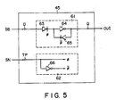
- the latch circuit 45 latches the "H"-level signal, i.e., data sensed by the sense amplifier.
- the sense amplifier after data is determined by the sense amplifier, the sense amplifier is disabled, reducing a feedthrough current. Therefore, wasteful current consumption can be decreased.
Landscapes
- Engineering & Computer Science (AREA)
- Microelectronics & Electronic Packaging (AREA)
- Computer Hardware Design (AREA)
- Static Random-Access Memory (AREA)
- Dram (AREA)
- Read Only Memory (AREA)
- Semiconductor Memories (AREA)
Applications Claiming Priority (2)
| Application Number | Priority Date | Filing Date | Title |
|---|---|---|---|
| JP1021004A JPH02201797A (ja) | 1989-01-31 | 1989-01-31 | 半導体メモリ装置 |
| JP21004/89 | 1989-01-31 |
Publications (3)
| Publication Number | Publication Date |
|---|---|
| EP0383080A2 true EP0383080A2 (fr) | 1990-08-22 |
| EP0383080A3 EP0383080A3 (fr) | 1991-06-26 |
| EP0383080B1 EP0383080B1 (fr) | 1994-04-06 |
Family
ID=12042936
Family Applications (1)
| Application Number | Title | Priority Date | Filing Date |
|---|---|---|---|
| EP90101625A Expired - Lifetime EP0383080B1 (fr) | 1989-01-31 | 1990-01-26 | Mémoire à semi-conducteur |
Country Status (5)
| Country | Link |
|---|---|
| US (1) | US5007024A (fr) |
| EP (1) | EP0383080B1 (fr) |
| JP (1) | JPH02201797A (fr) |
| KR (1) | KR930007279B1 (fr) |
| DE (1) | DE69007827T2 (fr) |
Cited By (11)
| Publication number | Priority date | Publication date | Assignee | Title |
|---|---|---|---|---|
| EP0490690A1 (fr) * | 1990-12-13 | 1992-06-17 | Mitsubishi Denki Kabushiki Kaisha | Circuit amplificateur |
| EP0600142A1 (fr) * | 1992-11-30 | 1994-06-08 | STMicroelectronics S.r.l. | Architecture à haute performance pour la génération de RAM à une seule porte |
| EP0621602A3 (fr) * | 1993-04-21 | 1995-05-17 | Plessey Semiconductors Ltd | Mémoire à accès aléatoire. |
| EP0690430A3 (fr) * | 1994-06-02 | 1996-07-03 | Accelerix Ltd | Mémoire de trame et accélérateur graphique monopuce |
| WO1997024726A1 (fr) * | 1995-12-28 | 1997-07-10 | Lsi Logic Corporation | Procede et equipement pour un systeme de commande de memoire de faible puissance a auto-synchronisation |
| EP0715310A3 (fr) * | 1994-11-30 | 1998-01-28 | Texas Instruments Incorporated | Améliorations relatives à des dispositifs de mémoire |
| EP0869506A1 (fr) * | 1997-04-03 | 1998-10-07 | STMicroelectronics S.r.l. | Dispositif de mémoire avec une dissipation de puissance réduite |
| US6041010A (en) * | 1994-06-20 | 2000-03-21 | Neomagic Corporation | Graphics controller integrated circuit without memory interface pins and associated power dissipation |
| EP0954864A4 (fr) * | 1997-11-25 | 2001-01-31 | Atmel Corp | Memoire a configuration haute vitesse et a consommation nulle |
| EP0632460B1 (fr) * | 1993-06-30 | 2001-09-19 | Sgs-Thomson Microelectronics, Inc. | Circuit de génération d'horloge avec compensation de variations de procédures de fabrication |
| US6490214B2 (en) * | 2000-12-26 | 2002-12-03 | Kabushiki Kaisha Toshiba | Semiconductor memory device |
Families Citing this family (23)
| Publication number | Priority date | Publication date | Assignee | Title |
|---|---|---|---|---|
| JP2789755B2 (ja) * | 1990-01-12 | 1998-08-20 | 日本電気株式会社 | 同期式半導体記憶装置 |
| JP3057780B2 (ja) * | 1991-03-06 | 2000-07-04 | 日本電気アイシーマイコンシステム株式会社 | 半導体集積回路 |
| JPH05266663A (ja) * | 1992-03-19 | 1993-10-15 | Fujitsu Ltd | 半導体記憶装置 |
| US5289415A (en) * | 1992-04-17 | 1994-02-22 | Motorola, Inc. | Sense amplifier and latching circuit for an SRAM |
| KR960011207B1 (ko) * | 1993-11-17 | 1996-08-21 | 김광호 | 반도체 메모리 장치의 데이타 센싱방법 및 그 회로 |
| GB2286072B (en) * | 1994-01-31 | 1998-02-25 | Advanced Risc Mach Ltd | Sense amplification in data memories |
| GB2286272A (en) * | 1994-01-31 | 1995-08-09 | Advanced Risc Mach Ltd | Data memory sense amplifier operation |
| US5481500A (en) * | 1994-07-22 | 1996-01-02 | International Business Machines Corporation | Precharged bit decoder and sense amplifier with integrated latch usable in pipelined memories |
| US5828245A (en) * | 1996-10-24 | 1998-10-27 | Stmicroelectronics, Inc. | Driver circuit including amplifier operated in a switching mode |
| US5708617A (en) * | 1997-01-28 | 1998-01-13 | Micron Technology, Inc. | Regressive drive sense amplifier |
| JP4059951B2 (ja) * | 1997-04-11 | 2008-03-12 | 株式会社ルネサステクノロジ | 半導体記憶装置 |
| US5973974A (en) * | 1997-09-09 | 1999-10-26 | Micro Technology, Inc. | Regressive drive sense amplifier |
| EP0944089A1 (fr) * | 1998-03-16 | 1999-09-22 | Nec Corporation | Dispositif de mémoire à semiconducteurs |
| JP2000243082A (ja) * | 1999-02-17 | 2000-09-08 | Mitsubishi Electric Corp | 半導体記憶装置 |
| CA2277717C (fr) * | 1999-07-12 | 2006-12-05 | Mosaid Technologies Incorporated | Circuit et methode de detection de correspondances multiples dans des memoires adressables par le contenu |
| JP4894095B2 (ja) * | 2001-06-15 | 2012-03-07 | 富士通セミコンダクター株式会社 | 半導体記憶装置 |
| ITRM20010531A1 (it) * | 2001-08-31 | 2003-02-28 | Micron Technology Inc | Dispositivo rilevatore a bassa potenza e alta tensione per memorie ditipo flash. |
| KR100454145B1 (ko) * | 2001-11-23 | 2004-10-26 | 주식회사 하이닉스반도체 | 플래쉬 메모리 장치 |
| KR100555521B1 (ko) * | 2003-10-28 | 2006-03-03 | 삼성전자주식회사 | 두 번 이상 샘플링하는 감지 증폭기를 구비하는 반도체 장치 및 반도체 장치의 데이터 판독 방법 |
| JP5343916B2 (ja) * | 2010-04-16 | 2013-11-13 | 富士通セミコンダクター株式会社 | 半導体メモリ |
| US8693264B2 (en) | 2012-02-21 | 2014-04-08 | Lsi Corporation | Memory device having sensing circuitry with automatic latching of sense amplifier output node |
| JP6752126B2 (ja) * | 2016-11-25 | 2020-09-09 | ラピスセミコンダクタ株式会社 | センスアンプ回路 |
| JP2024046318A (ja) * | 2022-09-22 | 2024-04-03 | 株式会社東芝 | センスアンプ回路および半導体記憶装置 |
Family Cites Families (12)
| Publication number | Priority date | Publication date | Assignee | Title |
|---|---|---|---|---|
| US4351034A (en) * | 1980-10-10 | 1982-09-21 | Inmos Corporation | Folded bit line-shared sense amplifiers |
| JPS60125998A (ja) * | 1983-12-12 | 1985-07-05 | Fujitsu Ltd | 半導体記憶装置 |
| US4715015A (en) * | 1984-06-01 | 1987-12-22 | Sharp Kabushiki Kaisha | Dynamic semiconductor memory with improved sense signal |
| JPH0736273B2 (ja) * | 1984-11-26 | 1995-04-19 | 株式会社日立製作所 | 半導体集積回路 |
| EP0189908B1 (fr) * | 1985-01-30 | 1992-10-28 | Nec Corporation | Mémoire dynamique comprenant un dispositif pour la précharge de lignes de bit |
| JPS61276198A (ja) * | 1985-04-26 | 1986-12-06 | アドバンスト・マイクロ・デイバイシズ・インコ−ポレ−テツド | Cmosメモリバイアスシステム |
| JPH0787032B2 (ja) * | 1985-07-08 | 1995-09-20 | 日本電気アイシ−マイコンシステム株式会社 | 半導体記憶装置 |
| JPS6286599A (ja) * | 1985-10-09 | 1987-04-21 | Nec Corp | 半導体記憶装置 |
| JPH0743938B2 (ja) * | 1985-10-09 | 1995-05-15 | 日本電気株式会社 | 差動増幅器 |
| JPS62197996A (ja) * | 1986-02-24 | 1987-09-01 | Toshiba Corp | 半導体メモリのセンスアンプ |
| JPS62197990A (ja) * | 1986-02-25 | 1987-09-01 | Mitsubishi Electric Corp | 半導体記憶回路 |
| JP2618938B2 (ja) * | 1987-11-25 | 1997-06-11 | 株式会社東芝 | 半導体記憶装置 |
-
1989
- 1989-01-31 JP JP1021004A patent/JPH02201797A/ja active Pending
-
1990
- 1990-01-18 US US07/466,920 patent/US5007024A/en not_active Expired - Lifetime
- 1990-01-26 EP EP90101625A patent/EP0383080B1/fr not_active Expired - Lifetime
- 1990-01-26 DE DE69007827T patent/DE69007827T2/de not_active Expired - Fee Related
- 1990-01-31 KR KR1019900001106A patent/KR930007279B1/ko not_active Expired - Lifetime
Cited By (23)
| Publication number | Priority date | Publication date | Assignee | Title |
|---|---|---|---|---|
| EP0490690A1 (fr) * | 1990-12-13 | 1992-06-17 | Mitsubishi Denki Kabushiki Kaisha | Circuit amplificateur |
| US5248946A (en) * | 1990-12-13 | 1993-09-28 | Mitsubishi Denki Kabushiki Kaisha | Symmetrical differential amplifier circuit |
| US5703821A (en) * | 1992-11-30 | 1997-12-30 | Sgs-Thomson Microelectronics S.R.L. | High performance single port RAM generator architecture |
| EP0600142A1 (fr) * | 1992-11-30 | 1994-06-08 | STMicroelectronics S.r.l. | Architecture à haute performance pour la génération de RAM à une seule porte |
| US5471428A (en) * | 1992-11-30 | 1995-11-28 | Sgs-Thomson Microelectronics S.R.L | High performance single port RAM generator architecture |
| EP0621602A3 (fr) * | 1993-04-21 | 1995-05-17 | Plessey Semiconductors Ltd | Mémoire à accès aléatoire. |
| EP0632460B1 (fr) * | 1993-06-30 | 2001-09-19 | Sgs-Thomson Microelectronics, Inc. | Circuit de génération d'horloge avec compensation de variations de procédures de fabrication |
| USRE40326E1 (en) | 1994-06-02 | 2008-05-20 | Mosaid Technologies Incorporated | Single chip frame buffer and graphics accelerator |
| US5694143A (en) * | 1994-06-02 | 1997-12-02 | Accelerix Limited | Single chip frame buffer and graphics accelerator |
| USRE44589E1 (en) | 1994-06-02 | 2013-11-12 | Mosaid Technologies Incorporated | Single chip frame buffer and graphics accelerator |
| USRE41565E1 (en) | 1994-06-02 | 2010-08-24 | Mosaid Technologies Incorporated | Single chip frame buffer and graphics accelerator |
| EP0690430A3 (fr) * | 1994-06-02 | 1996-07-03 | Accelerix Ltd | Mémoire de trame et accélérateur graphique monopuce |
| USRE37944E1 (en) | 1994-06-02 | 2002-12-31 | 3612821 Canada Inc. | Single chip frame buffer and graphics accelerator |
| US7106619B2 (en) | 1994-06-20 | 2006-09-12 | Neomagic Corporation | Graphics controller integrated circuit without memory interface |
| US6041010A (en) * | 1994-06-20 | 2000-03-21 | Neomagic Corporation | Graphics controller integrated circuit without memory interface pins and associated power dissipation |
| US6771532B2 (en) | 1994-06-20 | 2004-08-03 | Neomagic Corporation | Graphics controller integrated circuit without memory interface |
| US6920077B2 (en) | 1994-06-20 | 2005-07-19 | Neomagic Corporation | Graphics controller integrated circuit without memory interface |
| EP0715310A3 (fr) * | 1994-11-30 | 1998-01-28 | Texas Instruments Incorporated | Améliorations relatives à des dispositifs de mémoire |
| WO1997024726A1 (fr) * | 1995-12-28 | 1997-07-10 | Lsi Logic Corporation | Procede et equipement pour un systeme de commande de memoire de faible puissance a auto-synchronisation |
| EP0869506A1 (fr) * | 1997-04-03 | 1998-10-07 | STMicroelectronics S.r.l. | Dispositif de mémoire avec une dissipation de puissance réduite |
| US6061286A (en) * | 1997-04-03 | 2000-05-09 | Sgs-Thomson Miroelectronics S.R.L. | Memory device with reduced power dissipation |
| EP0954864A4 (fr) * | 1997-11-25 | 2001-01-31 | Atmel Corp | Memoire a configuration haute vitesse et a consommation nulle |
| US6490214B2 (en) * | 2000-12-26 | 2002-12-03 | Kabushiki Kaisha Toshiba | Semiconductor memory device |
Also Published As
| Publication number | Publication date |
|---|---|
| EP0383080A3 (fr) | 1991-06-26 |
| KR930007279B1 (ko) | 1993-08-04 |
| US5007024A (en) | 1991-04-09 |
| DE69007827D1 (de) | 1994-05-11 |
| JPH02201797A (ja) | 1990-08-09 |
| KR900012364A (ko) | 1990-08-03 |
| DE69007827T2 (de) | 1994-08-11 |
| EP0383080B1 (fr) | 1994-04-06 |
Similar Documents
| Publication | Publication Date | Title |
|---|---|---|
| EP0383080B1 (fr) | Mémoire à semi-conducteur | |
| US5029135A (en) | Semiconductor memory apparatus with internal synchronization | |
| US5777935A (en) | Memory device with fast write recovery and related write recovery method | |
| GB2287112A (en) | Auto-precharging semiconductor memory devices | |
| KR930008577B1 (ko) | 반도체 메모리장치 | |
| GB2226900A (en) | Memory timing circuit | |
| JPH0422318B2 (fr) | ||
| US5396463A (en) | Data output circuit of a semiconductor memory device | |
| US5506522A (en) | Data input/output line sensing circuit of a semiconductor integrated circuit | |
| EP0332135A3 (fr) | Circuit de mémoire non volatile ayant une faible consommation de courant et une plage de tension de fonctionnement étendue | |
| US5355343A (en) | Static random access memory with self timed bit line equalization | |
| JPS63304491A (ja) | 半導体メモリ | |
| JPS5755592A (en) | Memory device | |
| EP0420189B1 (fr) | Circuit amplificateur de détection | |
| US5737273A (en) | Sense amplifier and reading circuit with sense amplifier | |
| EP0874370A1 (fr) | circuit de commande pour amplificateur de lecture d'un circuit de mémoire | |
| US5754487A (en) | Bit line precharge circuit | |
| US20010000451A1 (en) | Voltage differential sensing circuit and methods of using same | |
| JPH0883491A (ja) | データ読出回路 | |
| KR0173832B1 (ko) | 부스트 회로 | |
| EP0409394A2 (fr) | Circuit de polarisation | |
| US4939392A (en) | Output circuit for driving a memory device output lead including a three-state inverting buffer and a transfer gate coupled between the buffer input lead and the buffer output lead | |
| US5438551A (en) | Semiconductor integrated circuit device | |
| US4435791A (en) | CMOS Address buffer for a semiconductor memory | |
| JPH0770224B2 (ja) | 同期式スタティックランダムアクセスメモリ |
Legal Events
| Date | Code | Title | Description |
|---|---|---|---|
| PUAI | Public reference made under article 153(3) epc to a published international application that has entered the european phase |
Free format text: ORIGINAL CODE: 0009012 |
|
| 17P | Request for examination filed |
Effective date: 19900126 |
|
| AK | Designated contracting states |
Kind code of ref document: A2 Designated state(s): DE FR GB |
|
| PUAL | Search report despatched |
Free format text: ORIGINAL CODE: 0009013 |
|
| AK | Designated contracting states |
Kind code of ref document: A3 Designated state(s): DE FR GB |
|
| 17Q | First examination report despatched |
Effective date: 19930709 |
|
| GRAA | (expected) grant |
Free format text: ORIGINAL CODE: 0009210 |
|
| AK | Designated contracting states |
Kind code of ref document: B1 Designated state(s): DE FR GB |
|
| REF | Corresponds to: |
Ref document number: 69007827 Country of ref document: DE Date of ref document: 19940511 |
|
| ET | Fr: translation filed | ||
| PLBE | No opposition filed within time limit |
Free format text: ORIGINAL CODE: 0009261 |
|
| STAA | Information on the status of an ep patent application or granted ep patent |
Free format text: STATUS: NO OPPOSITION FILED WITHIN TIME LIMIT |
|
| 26N | No opposition filed | ||
| REG | Reference to a national code |
Ref country code: GB Ref legal event code: IF02 |
|
| PGFP | Annual fee paid to national office [announced via postgrant information from national office to epo] |
Ref country code: DE Payment date: 20070118 Year of fee payment: 18 |
|
| PGFP | Annual fee paid to national office [announced via postgrant information from national office to epo] |
Ref country code: GB Payment date: 20070124 Year of fee payment: 18 |
|
| PGFP | Annual fee paid to national office [announced via postgrant information from national office to epo] |
Ref country code: FR Payment date: 20070109 Year of fee payment: 18 |
|
| GBPC | Gb: european patent ceased through non-payment of renewal fee |
Effective date: 20080126 |
|
| PG25 | Lapsed in a contracting state [announced via postgrant information from national office to epo] |
Ref country code: DE Free format text: LAPSE BECAUSE OF NON-PAYMENT OF DUE FEES Effective date: 20080801 |
|
| REG | Reference to a national code |
Ref country code: FR Ref legal event code: ST Effective date: 20081029 |
|
| PG25 | Lapsed in a contracting state [announced via postgrant information from national office to epo] |
Ref country code: GB Free format text: LAPSE BECAUSE OF NON-PAYMENT OF DUE FEES Effective date: 20080126 |
|
| PG25 | Lapsed in a contracting state [announced via postgrant information from national office to epo] |
Ref country code: FR Free format text: LAPSE BECAUSE OF NON-PAYMENT OF DUE FEES Effective date: 20080131 |