EP0383342A2 - Mikroprozessor - Google Patents
Mikroprozessor Download PDFInfo
- Publication number
- EP0383342A2 EP0383342A2 EP90103037A EP90103037A EP0383342A2 EP 0383342 A2 EP0383342 A2 EP 0383342A2 EP 90103037 A EP90103037 A EP 90103037A EP 90103037 A EP90103037 A EP 90103037A EP 0383342 A2 EP0383342 A2 EP 0383342A2
- Authority
- EP
- European Patent Office
- Prior art keywords
- register
- registers
- microprocessor
- set forth
- windows
- Prior art date
- Legal status (The legal status is an assumption and is not a legal conclusion. Google has not performed a legal analysis and makes no representation as to the accuracy of the status listed.)
- Granted
Links
Images


Classifications
-
- G—PHYSICS
- G06—COMPUTING OR CALCULATING; COUNTING
- G06F—ELECTRIC DIGITAL DATA PROCESSING
- G06F9/00—Arrangements for program control, e.g. control units
- G06F9/06—Arrangements for program control, e.g. control units using stored programs, i.e. using an internal store of processing equipment to receive or retain programs
- G06F9/22—Microcontrol or microprogram arrangements
-
- G—PHYSICS
- G06—COMPUTING OR CALCULATING; COUNTING
- G06F—ELECTRIC DIGITAL DATA PROCESSING
- G06F9/00—Arrangements for program control, e.g. control units
- G06F9/06—Arrangements for program control, e.g. control units using stored programs, i.e. using an internal store of processing equipment to receive or retain programs
- G06F9/46—Multiprogramming arrangements
- G06F9/50—Allocation of resources, e.g. of the central processing unit [CPU]
- G06F9/5005—Allocation of resources, e.g. of the central processing unit [CPU] to service a request
- G06F9/5011—Allocation of resources, e.g. of the central processing unit [CPU] to service a request the resources being hardware resources other than CPUs, Servers and Terminals
- G06F9/5016—Allocation of resources, e.g. of the central processing unit [CPU] to service a request the resources being hardware resources other than CPUs, Servers and Terminals the resource being the memory
-
- G—PHYSICS
- G06—COMPUTING OR CALCULATING; COUNTING
- G06F—ELECTRIC DIGITAL DATA PROCESSING
- G06F9/00—Arrangements for program control, e.g. control units
- G06F9/06—Arrangements for program control, e.g. control units using stored programs, i.e. using an internal store of processing equipment to receive or retain programs
- G06F9/30—Arrangements for executing machine instructions, e.g. instruction decode
- G06F9/30098—Register arrangements
- G06F9/3012—Organisation of register space, e.g. banked or distributed register file
- G06F9/30123—Organisation of register space, e.g. banked or distributed register file according to context, e.g. thread buffers
- G06F9/30127—Register windows
-
- G—PHYSICS
- G06—COMPUTING OR CALCULATING; COUNTING
- G06F—ELECTRIC DIGITAL DATA PROCESSING
- G06F9/00—Arrangements for program control, e.g. control units
- G06F9/06—Arrangements for program control, e.g. control units using stored programs, i.e. using an internal store of processing equipment to receive or retain programs
- G06F9/44—Arrangements for executing specific programs
- G06F9/448—Execution paradigms, e.g. implementations of programming paradigms
- G06F9/4482—Procedural
- G06F9/4484—Executing subprograms
-
- G—PHYSICS
- G06—COMPUTING OR CALCULATING; COUNTING
- G06F—ELECTRIC DIGITAL DATA PROCESSING
- G06F9/00—Arrangements for program control, e.g. control units
- G06F9/06—Arrangements for program control, e.g. control units using stored programs, i.e. using an internal store of processing equipment to receive or retain programs
- G06F9/46—Multiprogramming arrangements
- G06F9/461—Saving or restoring of program or task context
- G06F9/462—Saving or restoring of program or task context with multiple register sets
Definitions
- This invention relates to a microprocessor, and more particularly to a RISC (Reduced Instruction Computer Set) type microprocessor.
- RISC Reduced Instruction Computer Set
- microprocessor systems using a register window structure.
- program program using a procedure call many times
- many windows are used.
- the number of registers allotted or allocated to one window is fixed (hereinafter this will be called a fixing system).
- a fixing system the number of registers actually used in the individual procedure calls is less than the number of allocation.
- the fact that the number of allocation is fixed is very redundant. For this reason, there cannot be employed, e.g., such a method for effectively utilizing the register to allot a register which is not used in a current window to another window with a present window thus to increase the number of windows.
- This invention relates to a technology for constructing a microprocessor including a register window of the variable system.
- One of the objects is as follows. Namely, there is provided a technology for constructing a register window of the variable system to automatically determine the number of registers allotted to one window in dependency upon the content of the execution program of the processor.
- a technology for constructing a processor by a register window of the variable system capable of executing, as it is, a program developed for a microprocessor by a register window of the fixed system.
- the processing speed of the program of the background art is improved by reducing the overhead of overflow/underflow of the window without changing the content of the above-mentioned program.
- Another object is as follows. Namely, there is provided a technology to construct a microprocessor provided with an instruction for controlling the number of registers allocated to the window in an instruction set as a microprocessor using a register window of the variable system.
- the number of registers allotted to the window can be flexibly determined in dependency upon the scale of the number of registers using a procedure in the program.
- the microprocessor manufactured is convenient for use, the efficiency of using the windows is improved, overhead by overflow/underflow of the window is reduced, and the cost performance is excellent.
- the number of registers allocated to respective register windows (modules) is stored in the memory means.
- which registers, i.e., how many registers constitute each module is determined.
- the number of registers constituting each module varies in dependency upon the number of allocation in the memory means. Namely, in accordance with individual procedures on the program, a working register used on that procedure is determined and the number of registers constituting the working register is determined.
- memorization of the number of registers allocated to each register window is automatically carried out on the basis of the address information for the working register.
- the memorization of the number of allocation is carried out on the basis of one of the instructions that the CPU (the system itself) can execute.
- the number of registers allocated to the window (module) can be changed. For this reason, redundancy of the system is eliminated, thus making it possible to effectively utilize the hardware resources without loss. Furthermore, an excellent cost performance microprocessor based on the register window system can be provided.
- memorization of the number of registers allocated to registers of the register window is automatically carried out on the basis of the address information for the working register. For this reason, the existing program of the fixed system can be executed as it is and overhead by overflow/underflow of the window can be reduced.
- memorization of the number of allocation is carried out on the basis of one of instructions that the CPU (the system itself) can execute. For this reason, change in the number of allocation, etc. can be realized by software in dependency upon the scale of the registers used by the procedure in the program.
- This invention can therefore provide a microprocessor which has a higher efficiency in use of the registers, is more convenient, and has a higher cost performance than processors based on the fixed system by the background arts.
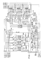
- FIG. 1 is a block diagram showing a microprocessor according to an embodiment of this invention. Specifically, there is shown the embodiment where the number of registers allocated to the locals and the outs of the window can be changed to eight or four.
- register addresses rs1-A0 to 4 designate a source register 1, a source register 2, and a destination register, respectively.
- Addresses A0 to 2 of the respective addresses are delivered to a R-FILE 1 module (first register) 101, a R-FILE 1 module (second register), and a R-FILE 2 module 103, respectively.
- These registers are comprised of multiport RAMs that are different from each other, respectively.
- addresses rs1-A0 to 2 addresses rs2-A0 to 2, and addresses rd-A0 to 4 are delivered to ports P0-A0 to 6 of each module, ports P1-A0 to 6, and ports P2-A0 to 6, respectively.
- Respective addresses A2 are delivered to a logic block 100.
- Addresses A3 to 4 of the respective addresses are delivered to decoders (DEC) 104, 105 and 106, respectively.
- DEC decoders
- rs1-D0 to 31 denote output data for the source register 1 and rs2-D0 to 31 denote output data for the source register 2. All of these rs1-D0 to 31 and rs2-D0 to 31 are outputted from respective ports P0-D0 to 31, P1-D0 to 31 of R-FILE 1 module 101, R-FILE 1 module 102, and R-FILE 2 module 103. Furthermore, rd-D0 to 31 are input data to the destination register, and these input data are delivered to respective ports P2-D0 to 31 of R-FILE 1 module 101, R-FILE 1 module 102 and R-FILE 2 module 103.
- the addresses labeled A0 to 4 designate 32 working registers of 8 globals and 24 registers (8 ins, 8 locals, 8 outs) constituting one window.
- Data labeled D0 to 31 are input/output data for the working register corresponding to addresses A0 to 4.
- Each of R-FILE 1 module 101, R-FILE 1 module 102 and R-FILE 2 module 103 constituting the working register is of a three-port structure consisting of two data output ports and one data input port. The addresses and data are independently connected to the respective ports of R-FILE 1 module 101, R-FILE 1 module 102 and R-FILE 2 module 103.
- the R-FILE 1 module 101 is a module of the register file constituting the working register of ins/outs, and is of a structure of 32 bits ⁇ 56 registers.
- the R-FILE 1 module 102 is a module of the register file constituting the working register of locals, and is of a structure of 32 bits ⁇ 56 registers.
- the R-FILE 2 module 103 is a module of the register file constituting the working register of globals, and is of a structure of 32 bits ⁇ 8 registers.
- ⁇ is an input terminal for clock CLK
- RE is an input terminal for read enable REGR-EN
- WE is an input terminal for write enable REGW-EN
- S0 to 2 are input terminals for signals for selecting respective ports.
- R-FILE 1 module 101 The internal area of R-FILE 1 module 101 is divided into 14 blocks addressed 0 to 13 as shown in FIG. 2, respectively. Furthermore, one block is composed of four registers. Addresses A3 to 6 of the port P0 (higher order 4 bits) are block addresses, respectively. Addresses A0 to 2 (lower order 3 bits) of the port P0 are addresses for eight registers each essentially comprised of a block designated by addresses A3 to 6 of the port P0. Addresses A0 to 6 of the port P1 and addresses A0 to 6 of the port P2 are the same as the above.
- a current window pointer (CWP) 107 outputs the number of a window used by the current procedure.
- This pointer is constructed as a binary counter of 5 bits which can perform an incremental operation on the basis of the increment signal INC.
- the current window pointer (CWP) forms 5 bits of lower order of the processor state register (PSR) in SPARC, the CWP employs a structure of 5 bits in conformity with the above in this embodiment.
- a register (W-CC) 108 is a register of 14 bits for storing information as to whether each window is in an eight register mode or in a four register mode. These 14 bits correspond to 14 windows, respectively. The bits “0" and “1” correspond to the eight register mode and the four register mode, respectively. When RESET is inputted, all bits are reset to "0". Thus, each window is set so that it is in the four mode. Switching to the eight register mode is automatically carried out as follows. Namely, working registers of outs and locals are divided into four first halves and four latter halves in the order of eight addresses, respectively. When only four outs and locals of the latter half are accessed by the procedure to shift to the next window, that window remains in the four register mode.
- any register of the first half is accessed in either outs or locals, a corresponding bit of the register (W-CC) 108 is set to "1".
- This window is brought into the eight register mode.
- the first half of locals corresponds to r16 to r19, the latter half thereof corresponds to r20 to r23, the first half of outs corresponds to r8 to r11, and the latter half thereof corresponds to r12 to r15.
- an enable signal rs1ccw-EN enables or permits rs1-A2 of the register address of the source register 1 to be used for setting register (W-CC) 108. Furthermore, an enable signal rs2CCW-EN enables rs2-A2 of the register address of the source register 2 to be used for setting the register (W-CC) 108. In addition, an enable signal rdCCW-EN enables rd-A2 of the register address of the destination register to be used for setting the register (W-CC) 108. These enable signals rs1CCW-EN, rs2CCW-EN, and rdCCW-EN are inputted to the logic block 100 to which respective addresses A2 are inputted.
- the logic block 100 outputs a set signal SET-CC for setting a specified bit or bits of the register (W-CC) 108 to "1".
- bit designation is carried out by CWP0 to 4 from the current window pointer (CWP) 107.
- the register (W-CC) 108 which has been subjected to bit designation by the set signal SET-CC from the logic block 100 and CWP0 to 4 from the current window pointer (CWP) 107 outputs a bit output ccn and a bit output ccn-1 to a current block pointer (CBP) 109.
- the bit output ccn represents the bit state of the register (W-CC) 108 corresponding to a current window
- the bit output ccn-1 represents the bit state of the register (W-CC) 108 corresponding to a previous window.
- Subtracters (INSAG) 110, 111 and 112 are subtracters of four bits for converting the block designation address for the R-FILE 1 module 101 of ins/outs from the value of outs to the value of ins when the register address designates ins, respectively. These subtracters are provided in correspondence with ports P0, P1, and P2 of the R-FILE 1 module 101, respectively.
- bit output ccn-1 is "1"
- respective values of output signals CbP0′0 to 3, CbP1′0 to 3, and CbP2′0 to 3 from the subtracters (INSAG) 110, 111 and 112 become CBP-2.
- out-rs1, out-rs2, and out-rd are outputted from the decoder (DEC) 104, the decoder (DEC) 105, and the decoder (DEC) 106, respectively.
- in-rs1, in-rs2 and in-rd, and out-rs1, rs2 and rd are processed at a logic block 200.
- the signals thus processed are outputted as enable signals for respective ports of the R-FILE 1 module 101 of IOSEL 0 to 2, and are inputted to input terminals S0 to 2 of the R-FILE 1 module 101.
- loc-rs1, loc-rs2, and loc-rd are outputted as enable signals for respective ports of the R-FILE 1 module 102, and are inputted to input terminals S0 to 2 of the R-FILE 1 module 102.
- glob-rs1l, glob-rs2, and glob-rd are outputted as enable signals for respective ports of the R-FILE 1 module 103, and are inputted to input terminals S0 to 2 of the R-FILE 1 module 103.
- the addresses r0 to 7, r8 to 15, r16 to 23, and r24 to 31 correspond to globals, outs, locals, and ins, respectively.
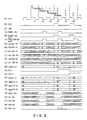
- FIG. 3A represents a clock CLK;
- FIG. 3B a decrement signal DEC;
- FIG. 3C an increment signal;
- FIG. 3D a read enable signals REGR-EN delivered to the R-FILE 1 module 101, the R-FILE 1 module 102, and the R-FILE 2 module 103;
- FIG. 3E a write enable signal REGW-EN delivered to the R-FILE 1 module 101, the R-FILE 1 module 102, and the R-FILE 2 module 103;
- FIG. 3A represents a clock CLK;
- FIG. 3B a decrement signal DEC;
- FIG. 3C an increment signal;
- FIG. 3D a read enable signals REGR-EN delivered to the R-FILE 1 module 101, the R-FILE 1 module 102, and the R-FILE 2 module 103;
- FIG. 3E a write enable signal REGW-EN delivered to the R-FILE 1 module 101, the R-FILE 1 module 102, and the R
- FIG. 3F enable signals rs1CCW-EN, rs2CCW-EN, and rdCCW-EN for enabling respective register addresses to be set at the register (W-CC) 108;
- FIG. 3J output data rs1-D0 to 31 from the source register 1;
- FIG. 3K output data rs2-D0 to 31 from the source register 2;
- FIG. 3L output data rd-D0 to 31 from the destination register;
- FIG. 3M outputs CWP0 to 4 from the current window pointer (CWP) 107;
- FIG. 3N a bit output ccn from the register (W-CC) 108;
- FIG. 30 a bit output ccn-1 from the register (W-CC) 108;
- FIG. 3P CbP0 to 3 which are outputs from the current block pointer (CBP) 109;
- FIG. 3Q CbP0′0 to 3 outputted from the subtracter (INSAG) 110;
- FIG. 3R CbP1′0 to 3 are outputted from the subtracter (INSAG) 111;
- FIG. 3S CbP2′0 to 3 are outputted from the subtracter (INSAG) 112;
- FIG. 3T a glob-rs1 are outputted from the decoder (DEC) 104;
- FIG. 3U an in-rs1 are outputted from the decoder (DEC) 104;
- FIG. 3V a loc-rs1 are outputted from the decoder (DEC) 104;
- FIG. 3W an out-rs1 are outputted from the decoder (DEC) 104;
- FIG. 3X a set signal SET-CC are outputted from the logic block 100.
- the period 1 represents ADD
- the period 2 represents SAVE
- the period 3 represents ADD
- the period 4 represents SAVE.
- r31 of rs1 and r12 of rs2 are added to r7 of rd, and the added result is shifted.
- the operation shifts to the next window, thus replacing CWP with CWP-1.
- r16 of rs1 and r12 of rs2 are added to r6 of rd, and the added result is shifted.
- save operation is performed. In this respect, it is assumed that 7, 3 and 2 are stored in [r31], [r12] and [r16], respectively.
- a pipe-line structure of four stages is employed.
- an ADD instruction is taken out from a memory 200 and is then written into an instruction register (IR) 202 (step F).
- the instruction in the instruction register (IR) 202 is inputted to an instruction decoder (IDEC) 204 and is then decoded thereat.
- An address for the next instruction is generated by an address generator (AG) 206 and a program counter (PC) 208.
- Register addresses rs1 and rs2 are read out from a register file (RF) 210, and are then written into an A register 212 and a B register 214, respectively (step D).
- step D of t4 data 2, 3 of r16 and r12 are outputted as data rs1-D0 to 31 and rs2-D0 to 31.
- the set output SET-CC becomes equal to "1".
- "1" is set at the bit 12 of the register (W-CC) 108.
- the window 12 is brought into the eight register mode.
- management of the number of allocation of locals and outs is conducted every blocks.
- the number of registers of locals and that of ins/outs are equal to each other, and locals and ins/outs are separately provided as different modules.
- the condition information per each window is sufficient to be one bit.
- the actual address generation circuit becomes simplified.
- calculation of the actual address can be carried out at a high speed.
- the number of registers to be allocated may be arbitrarily selected within a range of eight to zero registers. Furthermore, the number of registers allocated to locals and that allocated to outs may be different from each other.
Landscapes
- Engineering & Computer Science (AREA)
- Software Systems (AREA)
- Theoretical Computer Science (AREA)
- Physics & Mathematics (AREA)
- General Engineering & Computer Science (AREA)
- General Physics & Mathematics (AREA)
- Executing Machine-Instructions (AREA)
- Microcomputers (AREA)
- Devices For Executing Special Programs (AREA)
Applications Claiming Priority (2)
| Application Number | Priority Date | Filing Date | Title |
|---|---|---|---|
| JP1037805A JPH0630063B2 (ja) | 1989-02-17 | 1989-02-17 | マイクロプロセッサ |
| JP37805/89 | 1989-02-17 |
Publications (3)
| Publication Number | Publication Date |
|---|---|
| EP0383342A2 true EP0383342A2 (de) | 1990-08-22 |
| EP0383342A3 EP0383342A3 (de) | 1992-10-07 |
| EP0383342B1 EP0383342B1 (de) | 1996-08-28 |
Family
ID=12507729
Family Applications (1)
| Application Number | Title | Priority Date | Filing Date |
|---|---|---|---|
| EP90103037A Expired - Lifetime EP0383342B1 (de) | 1989-02-17 | 1990-02-16 | Mikroprozessor |
Country Status (5)
| Country | Link |
|---|---|
| US (1) | US5642523A (de) |
| EP (1) | EP0383342B1 (de) |
| JP (1) | JPH0630063B2 (de) |
| KR (1) | KR920006789B1 (de) |
| DE (1) | DE69028224T2 (de) |
Cited By (1)
| Publication number | Priority date | Publication date | Assignee | Title |
|---|---|---|---|---|
| EP0649090A1 (de) * | 1993-10-15 | 1995-04-19 | Kabushiki Kaisha Toshiba | Mikroprozessor mit Registerbankarchitektur |
Families Citing this family (8)
| Publication number | Priority date | Publication date | Assignee | Title |
|---|---|---|---|---|
| US5539911A (en) * | 1991-07-08 | 1996-07-23 | Seiko Epson Corporation | High-performance, superscalar-based computer system with out-of-order instruction execution |
| DE69924857T2 (de) * | 1998-10-10 | 2006-03-02 | Transitive Ltd., Hanging Ditch | Programm-kode-umwandlung |
| JP2000353092A (ja) * | 1999-06-09 | 2000-12-19 | Nec Corp | 情報処理装置及びそのレジスタファイル切替方法 |
| US6553487B1 (en) * | 2000-01-07 | 2003-04-22 | Motorola, Inc. | Device and method for performing high-speed low overhead context switch |
| JP3763518B2 (ja) | 2001-05-29 | 2006-04-05 | インターナショナル・ビジネス・マシーンズ・コーポレーション | コンパイラ、そのコンパイル方法およびプログラム |
| KR100718754B1 (ko) * | 2002-01-31 | 2007-05-15 | 에이알씨 인터내셔널 | 길이가 다른 명령어집합 구조를 갖는 설정가능형데이터프로세서 |
| US7127592B2 (en) * | 2003-01-08 | 2006-10-24 | Sun Microsystems, Inc. | Method and apparatus for dynamically allocating registers in a windowed architecture |
| JP2006039874A (ja) * | 2004-07-26 | 2006-02-09 | Fujitsu Ltd | 情報処理装置 |
Family Cites Families (5)
| Publication number | Priority date | Publication date | Assignee | Title |
|---|---|---|---|---|
| US4777588A (en) * | 1985-08-30 | 1988-10-11 | Advanced Micro Devices, Inc. | General-purpose register file optimized for intraprocedural register allocation, procedure calls, and multitasking performance |
| US5021947A (en) * | 1986-03-31 | 1991-06-04 | Hughes Aircraft Company | Data-flow multiprocessor architecture with three dimensional multistage interconnection network for efficient signal and data processing |
| JP2545789B2 (ja) * | 1986-04-14 | 1996-10-23 | 株式会社日立製作所 | 情報処理装置 |
| JPH0217541A (ja) * | 1988-07-06 | 1990-01-22 | Hitachi Ltd | スタツク方式マイクロコンピュータ |
| US5083263A (en) * | 1988-07-28 | 1992-01-21 | Sun Microsystems, Inc. | BISC with interconnected register ring and selectively operating portion of the ring as a conventional computer |
-
1989
- 1989-02-17 JP JP1037805A patent/JPH0630063B2/ja not_active Expired - Fee Related
-
1990
- 1990-02-16 DE DE69028224T patent/DE69028224T2/de not_active Expired - Fee Related
- 1990-02-16 EP EP90103037A patent/EP0383342B1/de not_active Expired - Lifetime
- 1990-02-17 KR KR1019900001965A patent/KR920006789B1/ko not_active Expired
-
1994
- 1994-08-09 US US08/287,428 patent/US5642523A/en not_active Expired - Fee Related
Non-Patent Citations (2)
| Title |
|---|
| ELECTRONIC DESIGN. vol. 36, no. 17, July 1988, HASBROUCK HEIGHTS, NEW JERSEY pages 49 - 58; MILT LEONARD: 'RISC microprocessors: many architectures thrive' * |
| IEEE MICRO. vol. 8, no. 2, April 1988, NEW YORK US BORIVOJE FURHT: 'A RISC Architecture with Two-size, Overlapping Register Windows' * |
Cited By (2)
| Publication number | Priority date | Publication date | Assignee | Title |
|---|---|---|---|---|
| EP0649090A1 (de) * | 1993-10-15 | 1995-04-19 | Kabushiki Kaisha Toshiba | Mikroprozessor mit Registerbankarchitektur |
| US5615348A (en) * | 1993-10-15 | 1997-03-25 | Kabushiki Kaisha Toshiba | Microprocessor having register bank architecture |
Also Published As
| Publication number | Publication date |
|---|---|
| EP0383342B1 (de) | 1996-08-28 |
| JPH0630063B2 (ja) | 1994-04-20 |
| EP0383342A3 (de) | 1992-10-07 |
| DE69028224T2 (de) | 1997-02-06 |
| DE69028224D1 (de) | 1996-10-02 |
| US5642523A (en) | 1997-06-24 |
| KR920006789B1 (ko) | 1992-08-17 |
| KR900013390A (ko) | 1990-09-05 |
| JPH02217925A (ja) | 1990-08-30 |
Similar Documents
| Publication | Publication Date | Title |
|---|---|---|
| US4361868A (en) | Device for increasing the length of a logic computer address | |
| US5881302A (en) | Vector processing unit with reconfigurable data buffer | |
| US4507728A (en) | Data processing system for parallel processing of different instructions | |
| EP0114304B1 (de) | Hardwarehilfe und Verfahren zur Vektorverarbeitung | |
| US4600986A (en) | Pipelined split stack with high performance interleaved decode | |
| US4016545A (en) | Plural memory controller apparatus | |
| EP0138451B1 (de) | Vektordaten-Verarbeitungssystem für indirekte Adressbefehle | |
| US4675806A (en) | Data processing unit utilizing data flow ordered execution | |
| US4334269A (en) | Data processing system having an integrated stack and register machine architecture | |
| GB2608979A (en) | Real-time control sequencer with state matrix logic | |
| US4446517A (en) | Microprogram memory with page addressing and address decode in memory | |
| EP0383342B1 (de) | Mikroprozessor | |
| EP0945783A2 (de) | Vorrichtung von Registern mit variablen Längen | |
| US6026486A (en) | General purpose processor having a variable bitwidth | |
| JPH06274528A (ja) | ベクトル演算処理装置 | |
| US4837688A (en) | Multi-channel shared resource processor | |
| US5867696A (en) | Saving a program counter value as the return address in an arbitrary general purpose register | |
| US6502182B1 (en) | Digital signal processing device | |
| JPS59106075A (ja) | デ−タ処理システム | |
| US6681319B1 (en) | Dual access instruction and compound memory access instruction with compatible address fields | |
| US4722052A (en) | Multiple unit adapter | |
| US20040205701A1 (en) | Computer system, virtual machine, runtime representation of object, storage media and program transmission apparatus | |
| CA2150518C (en) | Vector processing unit with reconfigurable data buffer | |
| EP1132813A2 (de) | Rechner mit schneller Kontextumschaltung | |
| US5388239A (en) | Operand address modification system |
Legal Events
| Date | Code | Title | Description |
|---|---|---|---|
| PUAI | Public reference made under article 153(3) epc to a published international application that has entered the european phase |
Free format text: ORIGINAL CODE: 0009012 |
|
| 17P | Request for examination filed |
Effective date: 19900216 |
|
| AK | Designated contracting states |
Kind code of ref document: A2 Designated state(s): DE FR GB |
|
| PUAL | Search report despatched |
Free format text: ORIGINAL CODE: 0009013 |
|
| AK | Designated contracting states |
Kind code of ref document: A3 Designated state(s): DE FR GB |
|
| 17Q | First examination report despatched |
Effective date: 19950411 |
|
| GRAH | Despatch of communication of intention to grant a patent |
Free format text: ORIGINAL CODE: EPIDOS IGRA |
|
| GRAA | (expected) grant |
Free format text: ORIGINAL CODE: 0009210 |
|
| GRAH | Despatch of communication of intention to grant a patent |
Free format text: ORIGINAL CODE: EPIDOS IGRA |
|
| AK | Designated contracting states |
Kind code of ref document: B1 Designated state(s): DE FR GB |
|
| REF | Corresponds to: |
Ref document number: 69028224 Country of ref document: DE Date of ref document: 19961002 |
|
| ET | Fr: translation filed | ||
| PGFP | Annual fee paid to national office [announced via postgrant information from national office to epo] |
Ref country code: GB Payment date: 19970207 Year of fee payment: 8 |
|
| PGFP | Annual fee paid to national office [announced via postgrant information from national office to epo] |
Ref country code: DE Payment date: 19970221 Year of fee payment: 8 |
|
| PLBE | No opposition filed within time limit |
Free format text: ORIGINAL CODE: 0009261 |
|
| STAA | Information on the status of an ep patent application or granted ep patent |
Free format text: STATUS: NO OPPOSITION FILED WITHIN TIME LIMIT |
|
| 26N | No opposition filed | ||
| PG25 | Lapsed in a contracting state [announced via postgrant information from national office to epo] |
Ref country code: GB Free format text: LAPSE BECAUSE OF NON-PAYMENT OF DUE FEES Effective date: 19980216 |
|
| GBPC | Gb: european patent ceased through non-payment of renewal fee |
Effective date: 19980216 |
|
| PG25 | Lapsed in a contracting state [announced via postgrant information from national office to epo] |
Ref country code: DE Free format text: LAPSE BECAUSE OF NON-PAYMENT OF DUE FEES Effective date: 19981103 |
|
| PGFP | Annual fee paid to national office [announced via postgrant information from national office to epo] |
Ref country code: FR Payment date: 20070208 Year of fee payment: 18 |
|
| REG | Reference to a national code |
Ref country code: FR Ref legal event code: ST Effective date: 20081031 |
|
| PG25 | Lapsed in a contracting state [announced via postgrant information from national office to epo] |
Ref country code: FR Free format text: LAPSE BECAUSE OF NON-PAYMENT OF DUE FEES Effective date: 20080229 |