EP0388565A1 - Chapeau de siliciure de métal réfractaire, pour protéger les structures multicouches de polycide - Google Patents
Chapeau de siliciure de métal réfractaire, pour protéger les structures multicouches de polycide Download PDFInfo
- Publication number
- EP0388565A1 EP0388565A1 EP89400830A EP89400830A EP0388565A1 EP 0388565 A1 EP0388565 A1 EP 0388565A1 EP 89400830 A EP89400830 A EP 89400830A EP 89400830 A EP89400830 A EP 89400830A EP 0388565 A1 EP0388565 A1 EP 0388565A1
- Authority
- EP
- European Patent Office
- Prior art keywords
- layer
- titanium
- silicide
- refractory metal
- forming
- Prior art date
- Legal status (The legal status is an assumption and is not a legal conclusion. Google has not performed a legal analysis and makes no representation as to the accuracy of the status listed.)
- Granted
Links
Images
Classifications
-
- H—ELECTRICITY
- H10—SEMICONDUCTOR DEVICES; ELECTRIC SOLID-STATE DEVICES NOT OTHERWISE PROVIDED FOR
- H10D—INORGANIC ELECTRIC SEMICONDUCTOR DEVICES
- H10D30/00—Field-effect transistors [FET]
- H10D30/01—Manufacture or treatment
- H10D30/021—Manufacture or treatment of FETs having insulated gates [IGFET]
- H10D30/0223—Manufacture or treatment of FETs having insulated gates [IGFET] having source and drain regions or source and drain extensions self-aligned to sides of the gate
-
- H—ELECTRICITY
- H10—SEMICONDUCTOR DEVICES; ELECTRIC SOLID-STATE DEVICES NOT OTHERWISE PROVIDED FOR
- H10D—INORGANIC ELECTRIC SEMICONDUCTOR DEVICES
- H10D64/00—Electrodes of devices having potential barriers
- H10D64/01—Manufacture or treatment
- H10D64/011—Manufacture or treatment of electrodes ohmically coupled to a semiconductor
- H10D64/0111—Manufacture or treatment of electrodes ohmically coupled to a semiconductor to Group IV semiconductors
- H10D64/0112—Manufacture or treatment of electrodes ohmically coupled to a semiconductor to Group IV semiconductors using conductive layers comprising silicides
-
- H—ELECTRICITY
- H10—SEMICONDUCTOR DEVICES; ELECTRIC SOLID-STATE DEVICES NOT OTHERWISE PROVIDED FOR
- H10D—INORGANIC ELECTRIC SEMICONDUCTOR DEVICES
- H10D64/00—Electrodes of devices having potential barriers
- H10D64/01—Manufacture or treatment
- H10D64/013—Manufacture or treatment of electrodes having a conductor capacitively coupled to a semiconductor by an insulator
- H10D64/01302—Manufacture or treatment of electrodes having a conductor capacitively coupled to a semiconductor by an insulator the insulator being formed after the semiconductor body, the semiconductor being silicon
- H10D64/01304—Manufacture or treatment of electrodes having a conductor capacitively coupled to a semiconductor by an insulator the insulator being formed after the semiconductor body, the semiconductor being silicon characterised by the conductor
- H10D64/01306—Manufacture or treatment of electrodes having a conductor capacitively coupled to a semiconductor by an insulator the insulator being formed after the semiconductor body, the semiconductor being silicon characterised by the conductor the conductor comprising a layer of silicon contacting the insulator, e.g. polysilicon
- H10D64/01308—Manufacture or treatment of electrodes having a conductor capacitively coupled to a semiconductor by an insulator the insulator being formed after the semiconductor body, the semiconductor being silicon characterised by the conductor the conductor comprising a layer of silicon contacting the insulator, e.g. polysilicon the conductor further comprising a non-elemental silicon additional conductive layer, e.g. a metal silicide layer formed by the reaction of silicon with an implanted metal
- H10D64/0131—Manufacture or treatment of electrodes having a conductor capacitively coupled to a semiconductor by an insulator the insulator being formed after the semiconductor body, the semiconductor being silicon characterised by the conductor the conductor comprising a layer of silicon contacting the insulator, e.g. polysilicon the conductor further comprising a non-elemental silicon additional conductive layer, e.g. a metal silicide layer formed by the reaction of silicon with an implanted metal the additional conductive layer comprising a silicide layer formed by the silicidation reaction between the layer of silicon with a metal layer which is not formed by metal implantation
-
- Y—GENERAL TAGGING OF NEW TECHNOLOGICAL DEVELOPMENTS; GENERAL TAGGING OF CROSS-SECTIONAL TECHNOLOGIES SPANNING OVER SEVERAL SECTIONS OF THE IPC; TECHNICAL SUBJECTS COVERED BY FORMER USPC CROSS-REFERENCE ART COLLECTIONS [XRACs] AND DIGESTS
- Y10—TECHNICAL SUBJECTS COVERED BY FORMER USPC
- Y10S—TECHNICAL SUBJECTS COVERED BY FORMER USPC CROSS-REFERENCE ART COLLECTIONS [XRACs] AND DIGESTS
- Y10S148/00—Metal treatment
- Y10S148/015—Capping layer
-
- Y—GENERAL TAGGING OF NEW TECHNOLOGICAL DEVELOPMENTS; GENERAL TAGGING OF CROSS-SECTIONAL TECHNOLOGIES SPANNING OVER SEVERAL SECTIONS OF THE IPC; TECHNICAL SUBJECTS COVERED BY FORMER USPC CROSS-REFERENCE ART COLLECTIONS [XRACs] AND DIGESTS
- Y10—TECHNICAL SUBJECTS COVERED BY FORMER USPC
- Y10S—TECHNICAL SUBJECTS COVERED BY FORMER USPC CROSS-REFERENCE ART COLLECTIONS [XRACs] AND DIGESTS
- Y10S148/00—Metal treatment
- Y10S148/019—Contacts of silicides
-
- Y—GENERAL TAGGING OF NEW TECHNOLOGICAL DEVELOPMENTS; GENERAL TAGGING OF CROSS-SECTIONAL TECHNOLOGIES SPANNING OVER SEVERAL SECTIONS OF THE IPC; TECHNICAL SUBJECTS COVERED BY FORMER USPC CROSS-REFERENCE ART COLLECTIONS [XRACs] AND DIGESTS
- Y10—TECHNICAL SUBJECTS COVERED BY FORMER USPC
- Y10S—TECHNICAL SUBJECTS COVERED BY FORMER USPC CROSS-REFERENCE ART COLLECTIONS [XRACs] AND DIGESTS
- Y10S148/00—Metal treatment
- Y10S148/147—Silicides
Definitions
- the present invention pertains in general to the formation of polycides and more particularly, to a capping layer for providing increased oxidation resistance and chemical stability of a polycide structure.
- one advantage provided by polycides is the enabling of higher temperature processing subsequent to their deposition. This is necessary when attempting to form a high quality interlevel oxide to serve as an insulating layer between the various metal layers which, in present technology, can exceed three to four layers of interconnects. Typically, such oxide layers require the use of a deposited glass that is reflowed at temperatures of between 800-900°C. Conventional metals such as aluminum, etc., will melt at this temperature.
- the use of a polycide provides a relatively stable material with a high melting point that will not go through phase changes during formation of the interlevel oxide.
- Refractory metals such as Titanium, Tungsten, Molybdenum, Tantalum, etc. have been utilized to form the refractory metal silicide. Although all of these metals provide good thermal and chemical stability, they vary somewhat in their resistive properties.
- the most desirable refractory metal silicide from the standpoint of circuit operation is titanium silicide, which silicide exhibits the lowest electrical resistivity. In fact, titanium silicide is one of the few refractory metals that exhibits a lower electrical resistivity than the elemental metal from which the silicide is formed.
- titanium silicide is not as resistant to oxidation as the other silicides. Therefore, any subsequent oxidation on the surface of the titanium silicide after formation thereof can result in a higher contact resistance for interconnections made from different levels to the silicide, which is a common problem that plagues most processing systems.
- silicides with much higher oxidation resistance and better chemical stability will solve this problem but these silicides don't exhibit the same resistance characteristics as titanium silicide. Therefore, there exists a need for improving the oxidation resistance of the silicide layer over that exhibited by titanium silicide without suffering any loss of conductive properties and chemical stability of the surface of the polycide.
- the present invention disclosed and claimed herein comprises a method for forming a polycide structure that has an oxidation resistant cap formed thereon.
- the method includes first forming a layer of polycrystalline silicon over a semiconductor substrate. This is followed by formation of a primary layer of refractory metal over the polycrystalline silicon layer. A composite layer of refractory metal silicide is then formed over the primary refractory metal.
- the composite refractory metal layer has a sheet resistance that is at least equal to or greater than the sheet resistance of the resultant silicide cf the primary refractory metal layer, and has a chemical stability and oxidation resistance that is greater than the silicide of the primary refractory metal layer.
- the refractory metal layer is then reacted with the underlying polysilicon to form the silicide thereof by consuming only a portion of the silicon in the polysilicon layer.
- the polycide structure is then defined by patterning and etching techniques.
- the primary refractory metal layer is formed from titanium and the composite refractory material is tantalum silicide, such that a layer of tantalum silicide is disposed over the titanium silicide in the resultant structure.
- the tantalum silicide layer has a much higher chemical stability and an increased resistance to oxidation as compared to the titanium silicide.
- a layer of gate-oxide is disposed under the polycrystalline silicon layer.
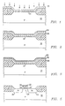
- FIGURE 1 there is illustrated a cross-sectional diagram of one step in the fabrication process for a semiconductor structure.
- a thin wafer of semiconductor material of one type conductivity such as that identified by reference numeral 10 in FIGURE 1
- the substrate 10 is P-type material.However, it should be understood that the opposite conductivity type material could be utilized.
- the oxide is then removed in a pattern to expose only those areas into which conductivity affecting impurities are to be diffused to form a "moat.”
- the substrate 10 is then subjected to diffusion of the desired impurities at temperatures suitable for such diffusion and, after the desired penetration and concentrations have been achieved and oxide regrown over the moat, the wafer is removed from the diffusion environment.
- a surface insulating layer 12, referred to as a field oxide of silicon results from oxide growth and diffusion steps in the process, thus creating a layer of sufficient thickness so that later, when the thin layers of metalization are applied, any electric fields developed in normal operation of the devices are insufficient to adversely affect operations of those portions of the semiconductor element, other than those where the insulating layer is intentionally thin.
- the silicon surface in the moat is exposed to various conventional clean-up steps and then a thin layer of gate-oxide 14 is grown over the moat to a thickness of between 100-1,000 Angstroms. This is referred to as the gate-oxide layer for an MOS transistor.
- the moat may be exposed down to "virgin" silicon and then the gate-oxide layer 14 formed on the surface thereof.
- a layer 16 of polycrystalline silicon (poly) is then deposited on the substrate by chemical vapor deposition (CVD) techniques to a thickness of approximately 2,000-4,000 ⁇ .
- N-type impurities are then diffused or implanted into the poly layer 16 to decrease the sheet resistance thereof to approximately 10-20 Ohms per square.
- phosphorus utilized as the N-type dopant is used as the N-type dopant.
- Titanium is a refractory metal, which as will be described hereinbelow, is converted to titanium silicide. Titanium silicide is widely used in the industry to provide a lower sheet resistance to long runs of poly.
- the poly layer 16 is necessary in order to provide a high integrity gate-oxide thereunder. At present, techniques are not available to deposit the refractory metal 18 directly onto the gate-oxide layer. Therefore, the poly layer 16 is utilized as a "buffer" whereas the later formed titanium silicide, formed from the layer of titanium 18, provides the desired conductive properties.
- the titanium layer 18 is deposited on the substrate by physical vapor deposition techniques. These techniques can either utilize a sputtering process or an evaporation process. In the preferred embodiment, the titanium is sputtered on with a Varian 3190 sputtering machine. This typically occurs at a temperature of 100°C and in a vacuum to provide a thickness of titanium of approximately 800 ⁇ .
- FIGURE 3 there is illustrated a cross-sectional diagram of FIGURE 2 with a composite layer 20 of tantalum silicide (TaSi2) deposited on the substrate to a thickness of approximately 500 ⁇ .
- this layer of tantalum silicide is sputtered on in situ with the titanium.
- the substrate 10 is maintained in the sputtering machine under vacuum for both deposition of the titanium layer 18 and the tantalum silicide layer 20.
- the substrate is initially placed into the sputtering machine and then a conventional clean-up done on the upper surface of the polysilicon 16 by backsputtering.
- Two targets are placed in the sputtering machine, one comprised of titanium refractory metal and the other comprised of a composite material of tantalum silicide.
- the composite tantalum silicide material is silicon-rich. That is, the stoichiometry of the compound is therefore TaSi x wherein x varies between two and three; that is, the ratio of the two substances slightly exceeds 2:1.
- the titanium layer 18 is then deposited by sputtering at a temperature of approximately 100°C after drawing a vacuum in the machine. The amount of titanium deposited is a function of the setting of the controls on the machine and the duration of the deposition process. Thereafter, the second target of tantalum silicide is selected and this is then deposited by a similar process utilizing a temperature of approximately 400°C.
- the titanium and the tantalum silicide deposited in the same operation it is not necessary to have the titanium and the tantalum silicide deposited in the same operation.
- the titanium could be deposited by a different process such as evaporative deposition or in a separate sputtering machine and then the substrate placed in the sputtering machine for the tantalum silicide deposition.
- this could require a back-sputtering clean-up process prior to depositing the tantalum silicide.
- the substrate is removed from the sputtering machine and then a layer of photoresist spun onto the substrate.
- This photoresist is patterned to define the conductive structure which, in the present example, is the gate of an MOS transistor.
- the substrate is then subjected to a plasma etch which is operable to etch the unpatterned areas away to define a multi-layer polycide structure which is comprised of the patterned layer 20 of tantalum silicide, the patterned layer 18 of titanium, the patterned layer 16 of polysilicon and the patterned layer 14 of gate-oxide.
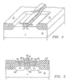
- FIGURE 4 depicts a perspective view of the gate of an MOS transistor. It can be seen that the gate of the transistor runs up over the field oxide layer 12 to provide interconnection with other circuitry.
- the etching of the polycide is achieved with dry etching (plasma or reactive ion etching) techniques which have been long accepted methods of etching polysilicon to provide integrated circuit gates/or interconnect levels.
- dry etching plasma or reactive ion etching
- the chemistry to provide anisotropic etching of polysilicon with good differential etch rates with respect to silicon dioxide is widely known.
- methods for etching of polycides are also well known. This type of etching is primarily directed to defining vertical edges on the patterned structures.
- One technique for etching polycides is disclosed in U.S. Patent No. 4,659,426, issued to Fuller, et.
- the substrate is subjected to a rapid isothermal annealing process in an N2 ambient.
- a rapid isothermal annealing process in an N2 ambient.
- this is a two-step process.
- the substrate is subjected to a temperature of between 550-650°C for a duration of approximately one minute.
- the substrate 10 with the defined polycide structure is then subjected to a temperature of 800-900°C, typically 900°C, for a duration of approximately twenty seconds.
- the purpose of this annealing process is to convert the titanium in layer 18 to titanium silicide by consuming a portion of the underlying poly layer 16.
- the formation of the titanium silicide is a conventional process.
- the titanium layer 18 consumes approximately 1,500 2,000 ⁇ of the silicon in the underlying poly layer 16. As illustrated in FIGURE 5, this results in formation of a titanium silicide layer 22 that is approximately 2,000 ⁇ thick. This leaves a poly layer 16 that is approximately 1,500 ⁇ thick.
- the purpose of subjecting the substrate to the 550-650°C temperature for one minute is to insure that there is minimum grain boundary diffusion during the silicidation process. This allows the N2 to go through the grain boundary and retard this rain boundary diffusion.
- the result is that the silicidation process at the temperature of 900°C is relatively slow and smooth as compared to a normal silicidation process. Since the silicidation process is relatively quick, there could be spiking at the polycide/oxide interface with the gate-oxide layer 14. This is an undesirable result, and the processing at the 550-650°C temperature retards this somewhat. Silicidation takes place at the 900°C temperature.
- the preferred embodiment is practiced by formation of the titanium silicide adjacent the polycrystalline silicon after the patterning and etching step, it should be understood that it is possible to subject the substrate to a temperature in excess of 850-900°C prior to the etching and patterning process to silicide before patterning.
- the titanium silicide can be formed prior to deposition of the tantalum silicide. It is only important that the tantalum silicide layer 20 be formed over the titanium silicide layer 22 in the resulting product.
- the tantalum silicide layer 20 although a silicided refractory material, differs from titanium silicide in that it is much more resistant to oxidation, which is one of the important aspects of the present invention.
- straight deposition of the tantalum silicide layer 20 over the polysilicon layer 16 to form the primary conductive coating is not as desirable as having titanium silicide, since titanium silicide has lower resistance than tantalum silicide.
- the refractory metal silicide utilized for the layer 20 which layer comprises a "capping" layer, the properties of that layer will vary. It is only important that the layer be more tolerant to oxidation than the titanium silicide layer 22. Therefore, the titanium silicide layer 22 is selected for providing the lowest sheet resistance with the layer 20 selected for providing the highest resistance to oxidation and optimum chemical stability for later processing.
- a refractory metal silicide can be utilized to provide a low-resistance layer without any substantial concern about its chemical stability and oxidation resistance.
- a second and capping layer can then be selected from the refractory metal silicides primarily for its chemical stability and oxidation resistance.
- This provides a technical advantage in that the processing steps can utilize the stability of the refractory metal silicides for such operations as forming interlevel oxides at temperatures in excess of 800°C, while providing a highly oxidation-resistant surface. This is important for forming contacts from a metalization layer to the tantalum silicide or capping layer 20. The formation of oxide on this layer would be undesirable since it would result in an increased contact resistance.
- the processing is then completed to form the transistor. This is done by conventional techniques.
- the source/drains are formed by implanting N-type impurities, such as phosphorus and arsenic, into the substrate on either side of the patterned polycide gate structure. This results in a source 24 and a drain 26, being formed on either side of the gate structure. A channel region 28 is thereby formed underlying the gate-oxide layer 14 between the source and drain structures 24 and 26 respectively. This structure is illustrated in FIGURE 5.
- FIGURE 6 after formation of the source 24 and drain 26, a layer of interlevel oxide 30 is deposited over the substrate to provide an insulating layer.
- An opening 32 is formed over the source 24, an opening 34 is formed over the drain 26 and an opening 36 is formed over the layer 20 in the gate structure.
- the opening 36 is typically offset from the openings 32 and 34 and over the field oxide layer 12.
- a source contact or plug 38 is formed in the opening 32 and a drain plug 40 is formed in the opening 34 and a gate plug 42 is formed in the opening 36 to contact the underlying conductive structures.
- the plugs 38-42 can be formed from a CVD deposition of such materials as polysilicon or tungsten. Thereafter, a layer of metalization such as aluminum is deposited and patterned on the upper surface of the interlevel oxide layer 30. This comprises a level of metalization.
- a process for forming a polycide structure that includes a titanium silicide layer overlying a layer of polysilicon and a gate-oxide layer.
- a capping layer of tantalum silicide or refractory metal silicide that is more oxidation resistant and that has a higher chemical stability than the titanium silicide is then formed over the titanium silicide.
- the process includes first forming the layer of titanium over the polysilicon followed by the deposition of a layer of tantalum silicide. This multi-layer polycide structure is then patterned and etched and then subjected to an annealing process to form titanium silicide from the titanium and underlying polysilicon material.
Landscapes
- Electrodes Of Semiconductors (AREA)
- Internal Circuitry In Semiconductor Integrated Circuit Devices (AREA)
Priority Applications (2)
| Application Number | Priority Date | Filing Date | Title |
|---|---|---|---|
| DE1989626616 DE68926616T2 (de) | 1989-03-24 | 1989-03-24 | Schwerschmelzende Metallsilicid-Verkapselung, zum Schutz mehrlagiger Policide |
| EP95203084A EP0704883A3 (fr) | 1988-02-11 | 1989-03-24 | Chapeau de siliciure de métal réfractaire, pour protéger les structures multicouches de polycide |
Applications Claiming Priority (2)
| Application Number | Priority Date | Filing Date | Title |
|---|---|---|---|
| US15480888A | 1988-02-11 | 1988-02-11 | |
| US07/357,666 US4886764A (en) | 1988-02-11 | 1989-05-25 | Process for making refractory metal silicide cap for protecting multi-layer polycide structure |
Related Child Applications (1)
| Application Number | Title | Priority Date | Filing Date |
|---|---|---|---|
| EP95203084.9 Division-Into | 1989-03-24 |
Publications (2)
| Publication Number | Publication Date |
|---|---|
| EP0388565A1 true EP0388565A1 (fr) | 1990-09-26 |
| EP0388565B1 EP0388565B1 (fr) | 1996-06-05 |
Family
ID=26851798
Family Applications (2)
| Application Number | Title | Priority Date | Filing Date |
|---|---|---|---|
| EP89400830A Expired - Lifetime EP0388565B1 (fr) | 1988-02-11 | 1989-03-24 | Chapeau de siliciure de métal réfractaire, pour protéger les structures multicouches de polycide |
| EP95203084A Withdrawn EP0704883A3 (fr) | 1988-02-11 | 1989-03-24 | Chapeau de siliciure de métal réfractaire, pour protéger les structures multicouches de polycide |
Family Applications After (1)
| Application Number | Title | Priority Date | Filing Date |
|---|---|---|---|
| EP95203084A Withdrawn EP0704883A3 (fr) | 1988-02-11 | 1989-03-24 | Chapeau de siliciure de métal réfractaire, pour protéger les structures multicouches de polycide |
Country Status (2)
| Country | Link |
|---|---|
| US (1) | US4886764A (fr) |
| EP (2) | EP0388565B1 (fr) |
Cited By (1)
| Publication number | Priority date | Publication date | Assignee | Title |
|---|---|---|---|---|
| EP0491433A3 (en) * | 1990-12-19 | 1992-09-02 | N.V. Philips' Gloeilampenfabrieken | Method of forming conductive region on silicon semiconductor material, and silicon semiconductor device with such region |
Families Citing this family (31)
| Publication number | Priority date | Publication date | Assignee | Title |
|---|---|---|---|---|
| US4978637A (en) * | 1989-05-31 | 1990-12-18 | Sgs-Thomson Microelectronics, Inc. | Local interconnect process for integrated circuits |
| US5679968A (en) * | 1990-01-31 | 1997-10-21 | Texas Instruments Incorporated | Transistor having reduced hot carrier implantation |
| US5094981A (en) * | 1990-04-17 | 1992-03-10 | North American Philips Corporation, Signetics Div. | Technique for manufacturing interconnections for a semiconductor device by annealing layers of titanium and a barrier material above 550° C. |
| US5443996A (en) * | 1990-05-14 | 1995-08-22 | At&T Global Information Solutions Company | Process for forming titanium silicide local interconnect |
| EP0483375B1 (fr) * | 1990-05-15 | 1996-03-13 | Kabushiki Kaisha Toshiba | Cible de pulverisation et production de cette derniere |
| US5034348A (en) * | 1990-08-16 | 1991-07-23 | International Business Machines Corp. | Process for forming refractory metal silicide layers of different thicknesses in an integrated circuit |
| EP0517368B1 (fr) * | 1991-05-03 | 1998-09-16 | STMicroelectronics, Inc. | Interconnexion locale pour circuits intégrés |
| US5332913A (en) * | 1991-12-17 | 1994-07-26 | Intel Corporation | Buried interconnect structure for semiconductor devices |
| KR950009283B1 (ko) * | 1992-08-24 | 1995-08-18 | 삼성전자주식회사 | 반도체장치의 제조방법 |
| US5409847A (en) * | 1993-10-27 | 1995-04-25 | Matsushita Electric Industrial Co., Ltd. | Manufacturing method of CMOS transistor in which heat treatment at higher temperature is done prior to heat treatment at low temperature |
| US5438006A (en) * | 1994-01-03 | 1995-08-01 | At&T Corp. | Method of fabricating gate stack having a reduced height |
| US5476803A (en) * | 1994-10-17 | 1995-12-19 | Liu; Kwo-Jen | Method for fabricating a self-spaced contact for semiconductor devices |
| JP3072754B2 (ja) * | 1994-10-18 | 2000-08-07 | シャープ株式会社 | 半導体装置の製造方法 |
| JPH08148561A (ja) * | 1994-11-16 | 1996-06-07 | Mitsubishi Electric Corp | 半導体装置とその製造方法 |
| US5895255A (en) * | 1994-11-30 | 1999-04-20 | Kabushiki Kaisha Toshiba | Shallow trench isolation formation with deep trench cap |
| US5593924A (en) * | 1995-06-02 | 1997-01-14 | Texas Instruments Incorporated | Use of a capping layer to attain low titanium-silicide sheet resistance and uniform silicide thickness for sub-micron silicon and polysilicon lines |
| JPH0974195A (ja) * | 1995-07-06 | 1997-03-18 | Mitsubishi Electric Corp | 半導体装置および半導体装置の製造方法 |
| US5635765A (en) * | 1996-02-26 | 1997-06-03 | Cypress Semiconductor Corporation | Multi-layer gate structure |
| US5767558A (en) * | 1996-05-10 | 1998-06-16 | Integrated Device Technology, Inc. | Structures for preventing gate oxide degradation |
| US5798296A (en) * | 1996-05-17 | 1998-08-25 | Micron Technology, Inc. | Method of fabricating a gate having a barrier of titanium silicide |
| TW316326B (en) * | 1996-09-21 | 1997-09-21 | United Microelectronics Corp | Manufacturing method of word line |
| EP0836223A3 (fr) * | 1996-10-08 | 1999-12-15 | Texas Instruments Inc. | Méthode de fabrication d'une couche de silicure |
| US5956614A (en) * | 1996-12-17 | 1999-09-21 | Texas Instruments Incorporated | Process for forming a metal-silicide gate for dynamic random access memory |
| US5851891A (en) * | 1997-04-21 | 1998-12-22 | Advanced Micro Devices, Inc. | IGFET method of forming with silicide contact on ultra-thin gate |
| US5985768A (en) * | 1997-04-30 | 1999-11-16 | International Business Machines Corporation | Method of forming a semiconductor |
| US7282443B2 (en) * | 2003-06-26 | 2007-10-16 | Micron Technology, Inc. | Methods of forming metal silicide |
| US7125815B2 (en) | 2003-07-07 | 2006-10-24 | Micron Technology, Inc. | Methods of forming a phosphorous doped silicon dioxide comprising layer |
| US8207064B2 (en) * | 2009-09-17 | 2012-06-26 | Sandisk 3D Llc | 3D polysilicon diode with low contact resistance and method for forming same |
| US9536830B2 (en) | 2013-05-09 | 2017-01-03 | Globalfoundries Inc. | High performance refractory metal / copper interconnects to eliminate electromigration |
| US9171801B2 (en) | 2013-05-09 | 2015-10-27 | Globalfoundries U.S. 2 Llc | E-fuse with hybrid metallization |
| US9305879B2 (en) | 2013-05-09 | 2016-04-05 | Globalfoundries Inc. | E-fuse with hybrid metallization |
Citations (1)
| Publication number | Priority date | Publication date | Assignee | Title |
|---|---|---|---|---|
| EP0053712A1 (fr) * | 1980-12-08 | 1982-06-16 | International Business Machines Corporation | Procédé pour l'amélioration de la conductivité d'un film microélectroniquement conducteur en siliciure de tungstène et dispositif semi-conducteur contenant ce film |
Family Cites Families (9)
| Publication number | Priority date | Publication date | Assignee | Title |
|---|---|---|---|---|
| US3537174A (en) * | 1968-10-07 | 1970-11-03 | Gen Electric | Process for forming tungsten barrier electrical connection |
| US4227944A (en) * | 1979-06-11 | 1980-10-14 | General Electric Company | Methods of making composite conductive structures in integrated circuits |
| US4263058A (en) * | 1979-06-11 | 1981-04-21 | General Electric Company | Composite conductive structures in integrated circuits and method of making same |
| GB2061615A (en) * | 1979-10-25 | 1981-05-13 | Gen Electric | Composite conductors for integrated circuits |
| US4445134A (en) * | 1980-12-08 | 1984-04-24 | Ibm Corporation | Conductivity WSi2 films by Pt preanneal layering |
| JPS61206243A (ja) * | 1985-03-08 | 1986-09-12 | Mitsubishi Electric Corp | 高融点金属電極・配線膜を用いた半導体装置 |
| US4657628A (en) | 1985-05-01 | 1987-04-14 | Texas Instruments Incorporated | Process for patterning local interconnects |
| US4659426A (en) | 1985-05-03 | 1987-04-21 | Texas Instruments Incorporated | Plasma etching of refractory metals and their silicides |
| JPS63165A (ja) * | 1986-06-19 | 1988-01-05 | Matsushita Electric Ind Co Ltd | 半導体装置の製造方法 |
-
1989
- 1989-03-24 EP EP89400830A patent/EP0388565B1/fr not_active Expired - Lifetime
- 1989-03-24 EP EP95203084A patent/EP0704883A3/fr not_active Withdrawn
- 1989-05-25 US US07/357,666 patent/US4886764A/en not_active Expired - Lifetime
Patent Citations (1)
| Publication number | Priority date | Publication date | Assignee | Title |
|---|---|---|---|---|
| EP0053712A1 (fr) * | 1980-12-08 | 1982-06-16 | International Business Machines Corporation | Procédé pour l'amélioration de la conductivité d'un film microélectroniquement conducteur en siliciure de tungstène et dispositif semi-conducteur contenant ce film |
Non-Patent Citations (3)
| Title |
|---|
| IBM TECHNICAL DISCLOSURE BULLETIN, vol. 25, no. 4, September 1982, pages 1920-1921, New York, US; D.R. CAMPBELL et al.: "Enhanced polycide structures" * |
| IBM TECHNICAL DISCLOSURE BULLETIN, vol. 27, no. 6, November 1984, page 3292, New York, US; S.D. PEARSON et al.: "Protection of a polysilicon gate containing a metal silicide during an annealing step" * |
| IBM TECHNICAL DISCLOSURE BULLETIN, vol. 28, no. 2, July 1985, pages 760-761, New York, US; "Process for annealing contamination-sensitive metal films" * |
Cited By (1)
| Publication number | Priority date | Publication date | Assignee | Title |
|---|---|---|---|---|
| EP0491433A3 (en) * | 1990-12-19 | 1992-09-02 | N.V. Philips' Gloeilampenfabrieken | Method of forming conductive region on silicon semiconductor material, and silicon semiconductor device with such region |
Also Published As
| Publication number | Publication date |
|---|---|
| US4886764A (en) | 1989-12-12 |
| EP0704883A2 (fr) | 1996-04-03 |
| EP0704883A3 (fr) | 1997-07-09 |
| EP0388565B1 (fr) | 1996-06-05 |
Similar Documents
| Publication | Publication Date | Title |
|---|---|---|
| EP0388565B1 (fr) | Chapeau de siliciure de métal réfractaire, pour protéger les structures multicouches de polycide | |
| US5208472A (en) | Double spacer salicide MOS device and method | |
| EP0680077B1 (fr) | Circuit intégré avec barrière de contact améliorée | |
| EP0279588B1 (fr) | Contact dans une perforation dans un semi-conducteur et procédé pour sa fabrication | |
| US5027185A (en) | Polycide gate FET with salicide | |
| US5610099A (en) | Process for fabricating transistors using composite nitride structure | |
| US6522001B2 (en) | Local interconnect structures and methods for making the same | |
| US6028359A (en) | Integrated circuit having amorphous silicide layer in contacts and vias and method of manufacture therefor | |
| US4707723A (en) | Semiconductor device using a refractory metal as an electrode and interconnection | |
| US4755480A (en) | Method of making a silicon nitride resistor using plasma enhanced chemical vapor deposition | |
| KR0143542B1 (ko) | 반도체 장치 및 그 제조 방법 | |
| US5981383A (en) | Method of fabricating a salicide layer of a device electrode | |
| US5238872A (en) | Barrier metal contact architecture | |
| JPH065667B2 (ja) | ドーパントの外拡散を禁止する方法及び半導体装置 | |
| JPH09199443A (ja) | 集積回路におけるランディングパッド構成体の製造方法 | |
| US5798296A (en) | Method of fabricating a gate having a barrier of titanium silicide | |
| US5866947A (en) | Post tungsten etch bank anneal, to improve aluminum step coverage | |
| US6156644A (en) | Method for forming interconnects for semiconductor devices using reaction control layers, and interconnects formed thereby | |
| EP0807967B1 (fr) | Résistance de titane diffusée et méthode de fabrication | |
| US5705442A (en) | Optimized tungsten contact plug process via use of furnace annealed barrier layers | |
| US5403768A (en) | Manufacturing method of a thin film resistor | |
| US5804506A (en) | Acceleration of etch selectivity for self-aligned contact | |
| US6140216A (en) | Post etch silicide formation using dielectric etchback after global planarization | |
| US4799992A (en) | Interlevel dielectric fabrication process | |
| US6291890B1 (en) | Semiconductor device having a silicide structure |
Legal Events
| Date | Code | Title | Description |
|---|---|---|---|
| PUAI | Public reference made under article 153(3) epc to a published international application that has entered the european phase |
Free format text: ORIGINAL CODE: 0009012 |
|
| 17P | Request for examination filed |
Effective date: 19900619 |
|
| AK | Designated contracting states |
Kind code of ref document: A1 Designated state(s): DE FR GB IT |
|
| 17Q | First examination report despatched |
Effective date: 19930315 |
|
| GRAH | Despatch of communication of intention to grant a patent |
Free format text: ORIGINAL CODE: EPIDOS IGRA |
|
| GRAA | (expected) grant |
Free format text: ORIGINAL CODE: 0009210 |
|
| AK | Designated contracting states |
Kind code of ref document: B1 Designated state(s): DE FR GB IT |
|
| XX | Miscellaneous (additional remarks) |
Free format text: TEILANMELDUNG 95203084.9 EINGEREICHT AM 13/11/95. |
|
| REF | Corresponds to: |
Ref document number: 68926616 Country of ref document: DE Date of ref document: 19960711 |
|
| ITF | It: translation for a ep patent filed | ||
| ET | Fr: translation filed | ||
| PLBE | No opposition filed within time limit |
Free format text: ORIGINAL CODE: 0009261 |
|
| STAA | Information on the status of an ep patent application or granted ep patent |
Free format text: STATUS: NO OPPOSITION FILED WITHIN TIME LIMIT |
|
| 26N | No opposition filed | ||
| PGFP | Annual fee paid to national office [announced via postgrant information from national office to epo] |
Ref country code: DE Payment date: 19980327 Year of fee payment: 10 |
|
| PG25 | Lapsed in a contracting state [announced via postgrant information from national office to epo] |
Ref country code: DE Free format text: LAPSE BECAUSE OF NON-PAYMENT OF DUE FEES Effective date: 20000101 |
|
| REG | Reference to a national code |
Ref country code: GB Ref legal event code: IF02 |
|
| PGFP | Annual fee paid to national office [announced via postgrant information from national office to epo] |
Ref country code: FR Payment date: 20020312 Year of fee payment: 14 |
|
| PGFP | Annual fee paid to national office [announced via postgrant information from national office to epo] |
Ref country code: GB Payment date: 20020327 Year of fee payment: 14 |
|
| PG25 | Lapsed in a contracting state [announced via postgrant information from national office to epo] |
Ref country code: GB Free format text: LAPSE BECAUSE OF NON-PAYMENT OF DUE FEES Effective date: 20030324 |
|
| GBPC | Gb: european patent ceased through non-payment of renewal fee |
Effective date: 20030324 |
|
| PG25 | Lapsed in a contracting state [announced via postgrant information from national office to epo] |
Ref country code: FR Free format text: LAPSE BECAUSE OF NON-PAYMENT OF DUE FEES Effective date: 20031127 |
|
| REG | Reference to a national code |
Ref country code: FR Ref legal event code: ST |
|
| PG25 | Lapsed in a contracting state [announced via postgrant information from national office to epo] |
Ref country code: IT Free format text: LAPSE BECAUSE OF NON-PAYMENT OF DUE FEES;WARNING: LAPSES OF ITALIAN PATENTS WITH EFFECTIVE DATE BEFORE 2007 MAY HAVE OCCURRED AT ANY TIME BEFORE 2007. THE CORRECT EFFECTIVE DATE MAY BE DIFFERENT FROM THE ONE RECORDED. Effective date: 20050324 |