EP0392530A2 - Treiberschaltung für eine bipolare Transistorvorrichtung mit isoliertem Gate - Google Patents
Treiberschaltung für eine bipolare Transistorvorrichtung mit isoliertem Gate Download PDFInfo
- Publication number
- EP0392530A2 EP0392530A2 EP90107022A EP90107022A EP0392530A2 EP 0392530 A2 EP0392530 A2 EP 0392530A2 EP 90107022 A EP90107022 A EP 90107022A EP 90107022 A EP90107022 A EP 90107022A EP 0392530 A2 EP0392530 A2 EP 0392530A2
- Authority
- EP
- European Patent Office
- Prior art keywords
- voltage
- gate
- current
- bipolar transistor
- drive circuit
- Prior art date
- Legal status (The legal status is an assumption and is not a legal conclusion. Google has not performed a legal analysis and makes no representation as to the accuracy of the status listed.)
- Granted
Links
Images


Classifications
-
- H—ELECTRICITY
- H03—ELECTRONIC CIRCUITRY
- H03K—PULSE TECHNIQUE
- H03K17/00—Electronic switching or gating, i.e. not by contact-making and –breaking
- H03K17/08—Modifications for protecting switching circuit against overcurrent or overvoltage
- H03K17/082—Modifications for protecting switching circuit against overcurrent or overvoltage by feedback from the output to the control circuit
- H03K17/0828—Modifications for protecting switching circuit against overcurrent or overvoltage by feedback from the output to the control circuit in composite switches
-
- H—ELECTRICITY
- H03—ELECTRONIC CIRCUITRY
- H03K—PULSE TECHNIQUE
- H03K2217/00—Indexing scheme related to electronic switching or gating, i.e. not by contact-making or -breaking covered by H03K17/00
- H03K2217/0036—Means reducing energy consumption
Definitions
- the present invention relates to a drive circuit for driving an IGBT (Insulated Gate Bipolar Transistor) device which is a semiconductor switching device and, more particularly, to the protection of an IGBT from an excess current.
- IGBT Insulated Gate Bipolar Transistor
- An IGBT device is characterized by a high breakdown voltage and a large current capacity similar to a bipolar transistor. Further, similar to a power MOSFET, the IGBT device has a high input impedance due to its insulation gate structure, so that it is also characterized by easiness in driving and rapid switching capability. Hence, the IGBT device has recently attracted attention as a new device having such characteristics.
- Devices named IGT, COMFET, GEMFET, MBT or BiFET are commercially available.
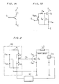
- Fig. 1A is a diagram showing a symbol of an IGBT device, including a gate G, a collector C and an emitter E.
- Fig. 1B is a circuit diagram showing an equivalent circuit of the IGBT device. Referring to Fig. 1B, the IGBT device has its gate G connected to a gate of a MOS transistor Q MOS and its emitter E connected to a source of the MOS transistor Q MOS . A pnp transistor Q1 and an npn transistor Q2 which make up a thyristor are inserted between the collector C and the emitter E.
- the transistor Q1 has its emitter connected to the collector C of the IGBT device and its base connected to a collector of the transistor Q2 and its collector connected to a base of the transistor Q2.
- the transistor Q2 has its collector connected to a drain of the MOS transistor Q MOS through a modulation resistor R M and its emitter connected to the emitter E of the IGBT device.
- a resistor R BE is connected between the base and emitter of the transistor Q2.
- a collector current I C is shoivn in Figs. 1A and 1B.
- the collector current I C of the IGBT device depends upon a gate voltage. If the gate voltage is above a predetermined value, the collector current would rise above the latch-up current to cause the latch-up.
- Fig. 2 is a circuit diagram showing a conventional drive circuit for the IGBT device.
- a switching unit SU is provided with voltage sources V GE1 and V GE2 .
- a negative potential terminal of the voltage source V GE1 and a positive potential terminal of the voltage source V GE2 are grounded.
- the positive potential terminal of the voltage source V GE1 is connected to an output point OUT via an output resistor R O and a switching element S1.
- the negative potential terminal of the voltage source V GE2 is connected to the output point OUT via a switching element S2.
- the output point OUT is connected to a gate of an IGBT device Q O via a gate resistor R G .
- the IGBT device Q O has its emitter grounded and its collector connected to a positive potential terminal of a voltage source V CC via a load LD and a current sensor CS. A negative potential terminal of the voltage source V CC is grounded.
- Capacities C GC and C GE exist between the gate and collector and between the gate and emitter as a parasitic capacity, respectively.
- An output of the current sensor CS is applied to control system.
- the control system SY performs its protecting operation to turn off the switching element S1 and to turn on the switching element S2, whereby the IGBT device Q O is forced into the OFF condition.
- a control signal from the control system SY decides the ON /OFF condition of the switching elements S1, S2.
- the IGBT device Q O turns on to supply current to the load LD.
- the IGBT device Q O turns off not to supply current to the load LD.
- the current supplied to the load LD is controlled by controlling the ON/OFF condition of the switching elements S1, S2.
- the supply voltage V CC could be directly applied to the collector of the IGBT device Q O due to an abnormal operation of the motor, as shown by a dotted line in Fig. 2. Since a voltage of several hundreds volt is used as the supply voltage V CC , the collector current I C is so rapidly increased as to cause the IGBT device Q O to generate heat. The collector current I C is further increased as the temperature of the IGBT device Q O goes up, so that the parasitic thyristor composed of the transistors Q1, Q2 shown in Fig. 1B can easily turn on. As a result, when the load LD becomes short circuited, latching-up due to a heat generation is liable to occur before the above-mentioned protection operation is executed by the control system SY.
- ⁇ V GE ⁇ V CE X C GC /C GE (1).
- the increased voltage ⁇ V CE is ranged approximately from tens of volts to hundreds of volts, and the capacity ratio C GC /C GE is approximately 0,01 - 0,05.
- ⁇ V GE 5V in accordance with the equation (1).
- the gate voltage is increased by 5V compared with the gate voltage at the normal operation, so that the collector current I C increases and latching-up may instantaneously occur.
- the gate voltage in the normal operation is reduced by using a low voltage of the voltage source V GE1 .
- the amount of a normal collector current I C is kept small in the IGBT device Q O , and therefore latch-up does not occur even if the collector current I C is increased by the short-circuited load LD.
- an increase of the ON state resistance of the IGBT device Q O aggravates power losses in circuit elements other than the load LD.
- a drive circuit for a conventional IGBT device structured as has been described drives the IGPT device Q O with the relatively low gate voltage not to latch-up the IGBT device Q O . Therefore, such a drive circuit has the disadvantages that the ON state resistance of the IGBT devices Q O is high, and that significant power loss is caused in the IGBT device Q O .
- a circuit in accordance with the present invention for driving an insulated gate bipolar transistor connected to a load to supply a current to the load comprises a forward gate bias power source for applying a forward gate bias voltage to the gate of the insulated gate bipolar transistor to drive the insulated gate bipolar transistor; a voltage lowering means connected the collector of the insulated gate bipolar transistor for lowering a voltage of the collector by a predetermined potential; a voltage divider connected between the voltage lowering means and the emitter of the insulated gate bipolar transistor, which has an intermediate point for providing a divided voltage; a current path disposed between the gate of the insulated gate bipolar transistor and a terminal having a predetermined voltage; a MOS transistor having its gate connected with the intermediate point of the divider and its source and drain serially disposed in the current path; and an output resistor connected between the gate of the insulated gate bipolar transistor and the forward gate bias power source.
- a MOS transistor which has its gate connected to an intermediate point of a voltage divider and its source and drain disposed in series in a current path provided between the gate of an insulated gate bopolar transistor and a terminal providing a predetermined potential, whereby the MOS transistor becomes conductive when a potential at a collector of the insulated gate bipolar transistor is above a predetermined potential to limit a gate potential of the insulated gate bipolar transistor.
- Fig. 3 is a circuit diagram of a drive circuit of an IGBT device according to an embodiment of the present invention.
- a switching unit SU is provided with voltage sources V GE1 , V GE2 .
- a negative potential terminal of the voltage source V GE1 and a positive potential terminal of the voltage source V GE2 are grounded.
- the positive potential terminal of the voltage source V GE1 is connected to an output point OUT via a output resistor R O and a switching element S1
- the negative potential terminal of the voltage source V GE2 is connected to the output point OUT via a switching element S2.
- the ON/OFF condition of the switching elements S1, S2 is designated.
- the output point OUT is connected to a gate of an IGBT device Q O via a gate resistor R G .
- the IGBT device Q O has its emitter grounded and its collector connected to a positive potential terminal of a voltage source V CC via a load LD and a current sensor CS. A negative potential terminal of the voltage source V CC is grounded. Further, capacities C GC and C GE exist between the gate and collector and between the gate and emitter as a parasitic capacity, respectively.
- An output of the current sensor CS is applied to a control system SY.
- the control system SY executes its protecting operation causing the switching element S1 to be in the OFF condition and the switching element S2 to be in the ON condition so as to force the IGBT device Q O to be in the OFF condition.
- a junction of the output resistor R O and the switching element S1 is connected to a drain of a MOS transistor Q M via a resistor R L .
- the source of the MOS transistor Q M is connected to the anode of diode D1, and the cathode of the diode D1 is connected to the ground potential.
- a current I L flows along the path in a direction shown in the Fig. 3.
- the diode D1 serves to prevent the current I L from flowing reversely.
- the resistor R L serves to limit the value of the current I L .
- the collector of the IGBT device Q O is connected to the anode of a diode D2, and the cathode of the diode D2 is connected to the cathede of a Zener diode D Z .
- Tne anode of the Zener diode D Z is grounded via resistors R1 and R2 serving as a potential dividers.
- a current I R flows along the path in a direction shown in the Fig. 3.
- the diode D2 serves to prevent the current I R from flowing reversely and is not essential.
- a junction of the resistor R1 and the resistor R2 is connected to the gate of the MOS transistor Q M .
- a flywheel diode D W is incorporated between the collector and the emitter of the IGBT device Q O usually in anti-parallel connection thereto.
- the flywheel diode D W has its anode connected to the emitter of the IGBT device Q O and its cathode connected to the collector. As can be seen, a collector current I C flows from the collector to the emitter in the IGBT device Q O .
- the whole drive circuit is structured as a bridge circuit consisting of a plurality of arms.
- the drive circuit shown in Fig. 3 corresponds to one of those arms, and other arms have similar construction. Wiring between the arms is so provided that a flywheel diode D X in another arm AR is connected to the opposite ends of the load LD in anti-parallel connection thereto.
- Figs. 4 and 5 are timing charts illustrating waveforms of each element of the drive circuit shown in Fig. 3 in its normal operation.
- the switching element S1 of Fig. 3 is in the OFF condition and the switching element S2 is in the ON condition.
- tile switching elements S1 and S2 are alternately switched ON/OFF and, in response to this, the IGBT device Q O is switched at a predetermined frequency.
- the negative potential terminal of the voltage source V GE2 is connected to the gate of the IGBT device Q O via the switching element S2 and the gate resistor R G .
- a negative voltage (-V GE2 ) is applied to cause the IGBT device Q O to turn off.
- no collector current I C flows, and supply voltage V CC is applied as a collector- emitter voltage V CE .
- the current I R is a reactive current for a period when the IGBT device Q O is in the OFF condition. Setting of a constant of each element for reducing the reactive current will be explained later.
- the switching element S1 is in the ON condition and the switching element S2 is in the OFF condition.
- the positive potential terminal of the voltage source V GE1 is conneted to the gate of the IGBT device Q O via the resistor R O , the switching element S1 and the gate resistor R G .
- the gate voltage V G goes up and reaches OV at a time t2.
- the gate voltage V G reaches a potential at which the IGBT device Q O becomes active, before time t3.
- the collector current I C begins to flow before a time t3.
- voltage V CE begins to go down since the IGBT device Q O turns from the OFF condition to the ON condition.
- the collector current I C is temporarily increased from the time t3 to the time t4 because of a reverse recovery current of the flywheel diode D X in the arm AR to reach a normal peak current I CPN . After that, it comes into a stationary state to reach a normal current value I CN determined depending upon the voltage of the voltage source V GE1 .
- the voltage V CE goes down from the time t3 to the time t4. After the time t4, it reaches a saturation voltage V CES since the IGBT device Q O reaches the complete ON condition.
- Figs. 6 and 7 are timing charts illustrating waveforms of each part of the drive circuit in the case of the short-circuit of the load.
- This conventional drive circuit is equivalent to a circuit in which a protection circuit consisting of the diodes D1, D2 and D Z , the resistors R1, R2 and R L and the MOS transistor Q M is eliminated unlike the circuit of Fig. 3 and, therefore, has no protection function.
- a waveform of the gate voltage V G in the case of the short-circuit of the load LD is identical with that of the gate voltage V G in the normal operation explained hereinbefore with reference to Fig. 4, in accordance with the ON/OFF condition of the switching elements S1 and S2 before the time t5.
- the gate voltage V G transiently goes up by a voltage increase ⁇ V GE in proportion to the capacity ratio C GC /C GE until the time t6. After that, the gate voltage V G goes down to the voltage of the positive potential terminal of the voltage source V GE1 to be in a stationary state.
- the collector current I C begins to flow before the time t3 in accordance with the rise of the gate voltage V G , and thereafter it is increased. It is temporarily increased in accordance with the increased amount of the voltage ⁇ V GE and reaches the peak current I CPS in the case of the short-circuit of the load LD at the time t6. It comes to a stationary state thereafter to reach a constant current value I CS in the case of the short-circuit of the load LD.
- the collector-emitter voltage V CE temporarily goes down from the supply voltage V CC because a small collector current I C flows and the collector-emitter resistance of the IGBT device Q O is also small. After that, as the collector current I C is increased, the collector-emitter resistance of the IGBT device Q O becomes large. Further, because the load LD is short-circuited, the collector-emitter voltage V CE goes up to the supply voltage V CC and almost reaches the supply voltage V CC in the stationary state after the time t6.
- the collector-emitter voltage V CE is maintained almost at the supply voltage V CC , and hence the current value I CS in the case of the short-circuit of the load LD is much larger than the normal current value I CN mentioned above with reference to Fig. 5, approximately 6 to 7 times, for example, as large as the rated current flowing in the normal operation.
- latch-up may be instantaneously caused in the IGBT device Q O because of a temporarily increased peak current I CPS in the case of the short-circuit of the load.
- latch-up may be caused by a current increase due to a heat generation as explained below.
- such a drive circuit is usually protected by the control system SY for controlling the switching elements S1, S2.
- the control system SY for controlling the switching elements S1, S2.
- the collector current I C having a current value I CS which is 6 to 7 times as large as the rated current flows even in the stationary state after the time t6, and therefore latch-up is caused by a heat generation in approximately 5 - 30 ⁇ sec. Consequently, the protection operation by the control system SY becomes insufficient.
- the operation before the time t4 is the same as that of the above-mentioned circuit without protection function.
- the collector-emitter voltage V CE of the IGBT device Q O is increased.
- the collector-emitter voltage V CE is larger than the sum of the Zener voltage V Z of the Zener diode D Z and a forward voltage V F of the diode D2
- the current I R flows in accordance with a characteristic shown in Fig. 8.
- the V - I characteristic assumes a monotonic increase although it depends upon the characteristics of the diodes D2 and D Z , and the current I R is increased in accordance with an increase in the voltage V CE .
- the gate voltage of the MOS transistor Q M is given by I R x R2.
- the collector-emitter voltage V CE rises above the threshold voltage V CET , the MOS transistor Q M turns on causing the current I L to flow.
- the voltage at the output point OUT in the switching unit SU that is, the gate voltage V G of the IGBT device Q O has the same value as that of a restricted gate voltage V GL given in accordance with the following equation (2):
- V GL I L x (R L + r DS ) + V F (2), where r DS is a drain-source resistance in the ON condition of the MOS transistor Q M .
- the peak current value of the collector current I C which flows when the collector-emitter voltage V CE reaches the threshold voltage V CET to start a restriction operation must be so small that latch-up may not be instantaneously caused in the IGBT device Q O .
- a constant of each element must be set so that the collector-emitter voltage V CE reaches a threshold voltage V CET and the MOS transistor Q M turns on before the time t6 when the peak current I CPS in the case of the short-circuit of the load flows and as early as possible after time t4.
- V CE collector-emitter voltage
- V CET threshold voltage
- MOS transistor Q M turns on before the time t6 when the peak current I CPS in the case of the short-circuit of the load flows and as early as possible after time t4.
- the threshold voltage V CET when the threshold voltage V CET is set excessively low so as to put forward the timing of starting the protection operation, the timing of starting the normal drive operation may be delayed or the protection operation mad be erroneously started due to noise or the like. Accordingly, the threshold voltage V CET must be set at a level where both the normal and protection operations can be smoothly performed. Setting of the timing of turning the MOS transistor Q M to the ON condition will be further explained later.
- the collector current I C at the protection operation is restricted to a sufficiently small current value I CL even if a significantly large supply voltage V CC is applied as a collector-emitter voltage V CE in the stationary state after the time t6.
- a period from the beginning of flow of an excess current to an occurence of latch-up due to a generated heat can be extended to be approximately 50 ⁇ sec by making the current value I CL approximately twice as large as the rated current flowing in the normal operation. In this way, the control system SY performs the above-mentioned protection operation effectively, and latch-up due to any generated heat can be prevented.
- the Zener diode D Z is provided as means for dropping voltage. With the Zener diode D Z , voltage across the resistors R1 and R2 is sufficiently smaller than the collector-emitter voltage V CE and, therefore, the current I R is also sufficiently small even if the supply voltage V CC is applied as the collector-emitter voltage V CE of the IGBT device Q O in the case of short-circuiting of the load LD or at the time of the OFF condition of the IGBT device Q O .
- a reactive current in the resistors R1 and R2 can be decreased and a power consumption can also be reduced by providing the Zener diode D Z as voltage dropping means.
- the Zener diode D Z Without the Zener diode D Z , a sufficiently large resistance value of the resistors R1 and R2 can make a power consumption in these resistors small.
- the gate voltage of the MOS transistor Q M depends upon a resistance value of the resistors R1 and R2.
- the timing where the gate voltage V G reaches a threshold voltage V TH that is, the timing of starting the protection operation also varies widely.
- a drive circuit which does not start an expected protection operation may be manufactured as a finished product.
- the resistors R1 and R2 of relatively small resistance value which have a small packaging area and can be formed with high accuracy, by employing the Zener diode D Z having a Zener voltage V Z according to the value of the supply voltage V CC or connecting a plurality of Zener diodes in series so as to make the voltage drop in this part of the circuit sufficiently large.
- the threshold voltage V TH of the MOS transistor Q M can be arbitrarily set by controlling the concentration of impurity ions injected into a channel region in manufacturing processes, for example.
- the threshold voltage V CET with which the protection function becomes available can be set more freely.
- a transient period necessary for turning the MOS transistor Q M from its OFF condition to the ON condition that is, a period from the application of the threshold voltage V TH to the gate of the MOS transistor Q M to the completion of turning on of the MOS transistor Q M is short so as to prevent latch-up due to the peak current I CPS in the case of the short-circuit of the load LD.
- the MOS transistor Q M may erroneously turn on in response to the normal peak current I CPN as explained below. That is, as shown in Fig. 5, during the period from the time t3 to the time t4 when the normal peak current I CPN flows, the collector-emitter voltage V CE has not yet sufficiently gone down and hence there is a high possibility that the diode D2 and the Zener diode D Z are in the ON condition. Hence, there is also a possibility that a part of the reverse recovery current flows as a part of the current I R and the gate voltage of the MOS transistor Q M temporarily goes up, so that the MOS transistor Q M might erroneously turn on.
- the threshold voltage V TH is set at such level that such an erroneous operation can not be caused. Meanwhile, such erroneous operation can be avoided assuredly by selecting the construction of the MOS transistor Q M as described below.
- Fig. 9A is a sectional view showing an example of a construction of a MOS transistor.
- a MOS transistor which has a vertical double diffused structure (VDMOS) shown in Fig. 9A is applied as the MOS transistor Q M .
- VDMOS transistor has the characteristics of a high voltage proof and a large current capacity. Further it has a structure which has a larger capacity of a gate electrode than the other structures have as described below.
- an n ⁇ type diffused region 2 which is connected to a drain electrode D is formed on an n+ type diffused region 1.
- the regions 1, 2 function as a drain.
- a p type diffused region 3 is formed in the n ⁇ type diffused region 2 and an n+ type diffused region 4 which functions as a source and is connected to a source electrode S is formed in the p type diffused region 3.
- a channel region 5 is formed in the surface of the p type diffused region 3 between the n+ type diffused region and the n ⁇ type diffused region 2 .
- a gate electrode 7 is formed on a gate oxide film 6.
- Fig. 9B is a diagram showing a plan view of a unit cell of the VDMOS transistor shown in Fig. 9A.
- the channel region 5 has a plane structure of a rectange each side of which is L in length and the size of the gate electrode 7 is decided in accordance with the length L.
- a MOS transistor having a large length L at the side of channel region 5 and a small resistance r DS between drain and source in its conductive state, that is, having a large current capacity and a gate electrode whose capacity is large is selected as the MOS transistor Q M .
- a MOS transistor Q M a drive circuit can be obtained in which needless protection operation can be avoided because the gate voltage does not remarkably go up with regard to the instantaneous peak current I CPN and the gate voltage sufficiently goes up with regard to the peak current I CPS in the case of the short-circuit of the load LD where an excess current continues to flow for more than a certain time so that necessary protection operation can be started.
- the capacity of the gate electrode 7 can be increased by forming many unit cells shown in Fig. 9B and connecting them in a parallel manner. Further, it can be increased by decreasing the thickness of the gate oxide film 6. or adjusting thickness of the oxide film on the gate electrode 7 or the junction capacity of the pn junction.
- the gate capacity can be controlled in a similar manner with respect to other structures, i.e., a comb type or hexagon type VDMOS transistor.
- a required period of time from the time t1 shown in Fig. 7 to the time t6 when the peak current I CPS flows is approximately 2 - 3 ⁇ sec.
- a required period of time from the time t1 shown in Fig. 5 to the time when the normal peak current I CPN flows is approximately 0,1 ⁇ sec in an IGBT device for a high frequency and approximatly 0,8 - 1,0 ⁇ sec in an IGBT device for a low frequency.
- the MOS transistor Q M can be turned on quite well without erroneous operation after the time when the normal peak current I CPN flows and until the time when the peak current I CPS in the case of the short-circuit of the load LD flows to prevent latch-up due to the peak current I CPS , by selecting the construction of the MOS transistor Q M , mainly controlling the gate capacity although the selection depends on whether the switching unit SU and load LD is for a high frequency or for a low frequency. That is, the MOS transistor having a small gate capacity is used when the IGBT device is for a high frequency and the MOS transistor having a large gate capacity is used when the IGBT device is for a low frequency.
Landscapes
- Electronic Switches (AREA)
- Power Conversion In General (AREA)
Applications Claiming Priority (2)
| Application Number | Priority Date | Filing Date | Title |
|---|---|---|---|
| JP93711/89 | 1989-04-13 | ||
| JP9371189 | 1989-04-13 |
Publications (3)
| Publication Number | Publication Date |
|---|---|
| EP0392530A2 true EP0392530A2 (de) | 1990-10-17 |
| EP0392530A3 EP0392530A3 (de) | 1991-12-11 |
| EP0392530B1 EP0392530B1 (de) | 1996-08-21 |
Family
ID=14090006
Family Applications (1)
| Application Number | Title | Priority Date | Filing Date |
|---|---|---|---|
| EP90107022A Expired - Lifetime EP0392530B1 (de) | 1989-04-13 | 1990-04-12 | Treiberschaltung für eine bipolare Transistorvorrichtung mit isoliertem Gate |
Country Status (3)
| Country | Link |
|---|---|
| US (1) | US5055721A (de) |
| EP (1) | EP0392530B1 (de) |
| DE (1) | DE69028131T2 (de) |
Cited By (6)
| Publication number | Priority date | Publication date | Assignee | Title |
|---|---|---|---|---|
| US5362980A (en) * | 1992-07-23 | 1994-11-08 | U.S. Philips Corporation | Semiconductor component with protective element for limiting current through component |
| DE4428675A1 (de) * | 1994-08-12 | 1996-02-15 | Siemens Ag | Schaltungsanordnung zum Schutz eines abschaltbaren Leistungshalbleiter-Schalters vor Überspannungen |
| EP0669658A3 (de) * | 1994-02-28 | 1999-10-06 | Mitsubishi Denki Kabushiki Kaisha | Feld-Effekt-Halbleiterbauelement und sein Herstellungsverfahren |
| EP0996227A3 (de) * | 1998-10-24 | 2001-03-28 | DaimlerChrysler AG | Verfahren zur Schaltzustandsüberwachung eines IGBT und Vorrichtung zur Durchführung des Verfahrens |
| CN103546020A (zh) * | 2013-10-28 | 2014-01-29 | 北京京铁信达铁路设备有限公司 | 高压igbt驱动及保护电路 |
| US9720030B2 (en) | 2015-06-08 | 2017-08-01 | Nxp Usa, Inc. | Systems and methods for testing a clamp function for insulated gate bipolar transistors |
Families Citing this family (31)
| Publication number | Priority date | Publication date | Assignee | Title |
|---|---|---|---|---|
| JPH0821620B2 (ja) * | 1990-05-21 | 1996-03-04 | 三菱電機株式会社 | 半導体装置 |
| FI90605C (fi) * | 1991-12-09 | 1994-02-25 | Abb Stroemberg Drives Oy | Puolijohdekytkimen ohjauspiiri |
| US5500619A (en) * | 1992-03-18 | 1996-03-19 | Fuji Electric Co., Ltd. | Semiconductor device |
| DE69207410T2 (de) * | 1992-09-18 | 1996-08-29 | Cons Ric Microelettronica | Monolithisch integrierte Brückenschaltung mit Transistoren und entsprechendes Herstellungsverfahren |
| US5347166A (en) * | 1993-02-01 | 1994-09-13 | Electric Power Research Institute | Apparatus and method for switching high power levels |
| JP3222330B2 (ja) * | 1994-09-20 | 2001-10-29 | 株式会社日立製作所 | 半導体回路及び半導体集積回路 |
| US5731729A (en) * | 1995-01-13 | 1998-03-24 | Ixys Corporation | Voltage transient suppression circuit for preventing overvoltages in power transistor systems |
| DE19512679C1 (de) * | 1995-04-07 | 1996-11-21 | Abb Management Ag | Stromleiteranordnung |
| JPH08308253A (ja) * | 1995-04-28 | 1996-11-22 | Mitsubishi Electric Corp | スイッチング半導体装置 |
| CA2172890C (en) * | 1995-06-06 | 2005-02-22 | Harold R. Schnetzka | Switch driver circuit |
| JP3373704B2 (ja) * | 1995-08-25 | 2003-02-04 | 三菱電機株式会社 | 絶縁ゲートトランジスタ駆動回路 |
| JP3469373B2 (ja) * | 1995-10-31 | 2003-11-25 | 三菱電機株式会社 | 半導体パワーモジュールおよび複合パワーモジュール |
| US5723916A (en) * | 1996-05-17 | 1998-03-03 | Delco Electronics Corporation | Electrical load driving device including load current limiting circuitry |
| US5847942A (en) * | 1996-05-30 | 1998-12-08 | Unitrode Corporation | Controller for isolated boost converter with improved detection of RMS input voltage for distortion reduction and having load-dependent overlap conduction delay of shunt MOSFET |
| JP3421507B2 (ja) * | 1996-07-05 | 2003-06-30 | 三菱電機株式会社 | 半導体素子の駆動回路 |
| CN1191394A (zh) * | 1997-02-20 | 1998-08-26 | 杨泰和 | 藉前置光-电转换元件驱动的绝缘栅双极晶体管 |
| JP3447949B2 (ja) * | 1998-03-31 | 2003-09-16 | 株式会社東芝 | 絶縁ゲート型半導体素子のゲート駆動回路、電力変換装置 |
| CN1312973A (zh) * | 1998-06-12 | 2001-09-12 | 南岛分立有限公司 | 绝缘栅功率半导体的栅极驱动 |
| JP3432425B2 (ja) * | 1998-08-05 | 2003-08-04 | 株式会社東芝 | ゲート回路 |
| US6809571B2 (en) * | 2001-10-01 | 2004-10-26 | International Rectifier Corporation | Power control circuit with active impedance to avoid interference and sensing problems |
| US6531895B1 (en) * | 2002-02-08 | 2003-03-11 | Delphi Technologies, Inc. | Isolated gate drive circuit having a switched input capacitor |
| US7768322B2 (en) * | 2004-10-12 | 2010-08-03 | Nxp B.V. | Low voltage, high-speed output-stage for laser or modulator driving |
| DE102007013824B4 (de) * | 2006-03-22 | 2013-10-24 | Denso Corporation | Schaltkreis mit einem Transistor |
| GB0617990D0 (en) * | 2006-09-13 | 2006-10-18 | Palmer Patrick R | Control of power semiconductor devices |
| US7466185B2 (en) * | 2006-10-23 | 2008-12-16 | Infineon Technologies Ag | IGBT-Driver circuit for desaturated turn-off with high desaturation level |
| DE112010003761T5 (de) * | 2009-09-15 | 2012-10-04 | Mitsubishi Electric Corporation | Gate-Ansteuerschaltung |
| IT1402879B1 (it) | 2010-11-19 | 2013-09-27 | St Microelectronics Srl | Dispositivo igbt con regioni di emettitore sepolte |
| JP5582123B2 (ja) * | 2011-10-05 | 2014-09-03 | 三菱電機株式会社 | 半導体装置 |
| DE102013216672A1 (de) * | 2013-08-22 | 2015-02-26 | Siemens Aktiengesellschaft | Elektronischer Schalter mit einem IGBT |
| CN105993122B (zh) * | 2013-11-29 | 2018-05-18 | 日产自动车株式会社 | 开关装置 |
| JP7749979B2 (ja) * | 2021-08-18 | 2025-10-07 | 富士電機株式会社 | 駆動装置 |
Family Cites Families (6)
| Publication number | Priority date | Publication date | Assignee | Title |
|---|---|---|---|---|
| US4301490A (en) * | 1979-07-09 | 1981-11-17 | American Standard Inc. | Electronic overload protection circuit |
| US4612457A (en) * | 1983-06-27 | 1986-09-16 | Texas Instruments Incorporated | Current limiting output buffer for integrated circuit |
| US4591734A (en) * | 1984-04-27 | 1986-05-27 | General Electric Company | Integratable circuit for controlling turn-off voltage rate-of-change of non-regenerative voltage-controlled switching semiconductor devices |
| EP0190925B1 (de) * | 1985-02-08 | 1993-12-29 | Kabushiki Kaisha Toshiba | Schutzschaltung für einen Bipolartransistor mit isoliertem Gate |
| JPS6395722A (ja) * | 1986-10-13 | 1988-04-26 | Fuji Electric Co Ltd | Igbt素子の過電流保護回路 |
| US4893158A (en) * | 1987-06-22 | 1990-01-09 | Nissan Motor Co., Ltd. | MOSFET device |
-
1989
- 1989-10-17 US US07/422,685 patent/US5055721A/en not_active Expired - Fee Related
-
1990
- 1990-04-12 EP EP90107022A patent/EP0392530B1/de not_active Expired - Lifetime
- 1990-04-12 DE DE69028131T patent/DE69028131T2/de not_active Expired - Fee Related
Cited By (7)
| Publication number | Priority date | Publication date | Assignee | Title |
|---|---|---|---|---|
| US5362980A (en) * | 1992-07-23 | 1994-11-08 | U.S. Philips Corporation | Semiconductor component with protective element for limiting current through component |
| EP0669658A3 (de) * | 1994-02-28 | 1999-10-06 | Mitsubishi Denki Kabushiki Kaisha | Feld-Effekt-Halbleiterbauelement und sein Herstellungsverfahren |
| DE4428675A1 (de) * | 1994-08-12 | 1996-02-15 | Siemens Ag | Schaltungsanordnung zum Schutz eines abschaltbaren Leistungshalbleiter-Schalters vor Überspannungen |
| EP0996227A3 (de) * | 1998-10-24 | 2001-03-28 | DaimlerChrysler AG | Verfahren zur Schaltzustandsüberwachung eines IGBT und Vorrichtung zur Durchführung des Verfahrens |
| CN103546020A (zh) * | 2013-10-28 | 2014-01-29 | 北京京铁信达铁路设备有限公司 | 高压igbt驱动及保护电路 |
| CN103546020B (zh) * | 2013-10-28 | 2016-08-31 | 北京京铁信达铁路设备有限公司 | 高压igbt驱动及保护电路 |
| US9720030B2 (en) | 2015-06-08 | 2017-08-01 | Nxp Usa, Inc. | Systems and methods for testing a clamp function for insulated gate bipolar transistors |
Also Published As
| Publication number | Publication date |
|---|---|
| DE69028131T2 (de) | 1997-03-06 |
| DE69028131D1 (de) | 1996-09-26 |
| EP0392530B1 (de) | 1996-08-21 |
| EP0392530A3 (de) | 1991-12-11 |
| US5055721A (en) | 1991-10-08 |
Similar Documents
| Publication | Publication Date | Title |
|---|---|---|
| EP0392530A2 (de) | Treiberschaltung für eine bipolare Transistorvorrichtung mit isoliertem Gate | |
| US4949213A (en) | Drive circuit for use with voltage-drive semiconductor device | |
| US6275093B1 (en) | IGBT gate drive circuit with short circuit protection | |
| JP3448340B2 (ja) | Igbt障害電流制限回路及び方法 | |
| US4286175A (en) | VMOS/Bipolar dual-triggered switch | |
| CA2267544C (en) | Gate control circuit for voltage drive switching element | |
| EP0467681A2 (de) | Treiberschaltung für einen Bipolartransistor mit isoliertem Gate mit Stromsonde | |
| US4954917A (en) | Power transistor drive circuit with improved short circuit protection | |
| CN114667681B (zh) | 栅极驱动电路 | |
| US6687106B1 (en) | Power module | |
| JPH02244904A (ja) | 誘導負荷駆動用パワーmosfet保護回路 | |
| US11831307B2 (en) | Power switch drive circuit and device | |
| JP3186619B2 (ja) | 内燃機関点火用回路装置および内燃機関点火用半導体装置 | |
| US5561393A (en) | Control device of semiconductor power device | |
| JPH07106934A (ja) | 半導体デバイスの過電流時のターンオフ回路装置 | |
| JP2913699B2 (ja) | 電圧駆動形半導体素子の駆動回路 | |
| USRE34107E (en) | Power transistor drive circuit with improved short circuit protection | |
| JP2007221473A (ja) | スイッチング回路の駆動回路及びスイッチング回路 | |
| JPH051652B2 (de) | ||
| US6160691A (en) | Method of driving a load and semiconductor load driver circuit therefor | |
| US5636097A (en) | Protective circuit for semiconductor power device | |
| EP0614278B1 (de) | Treiberschaltung für eine spannungsgesteuerte Halbleitervorrichtung | |
| JP2973997B2 (ja) | 電圧駆動形半導体素子の駆動回路 | |
| JP3325303B2 (ja) | 保護機能を備えたスイッチ装置 | |
| US4107552A (en) | Semiconductor switch |
Legal Events
| Date | Code | Title | Description |
|---|---|---|---|
| PUAI | Public reference made under article 153(3) epc to a published international application that has entered the european phase |
Free format text: ORIGINAL CODE: 0009012 |
|
| AK | Designated contracting states |
Kind code of ref document: A2 Designated state(s): DE FR GB |
|
| 17P | Request for examination filed |
Effective date: 19901212 |
|
| PUAL | Search report despatched |
Free format text: ORIGINAL CODE: 0009013 |
|
| AK | Designated contracting states |
Kind code of ref document: A3 Designated state(s): DE FR GB |
|
| 17Q | First examination report despatched |
Effective date: 19940607 |
|
| GRAH | Despatch of communication of intention to grant a patent |
Free format text: ORIGINAL CODE: EPIDOS IGRA |
|
| GRAH | Despatch of communication of intention to grant a patent |
Free format text: ORIGINAL CODE: EPIDOS IGRA |
|
| GRAA | (expected) grant |
Free format text: ORIGINAL CODE: 0009210 |
|
| AK | Designated contracting states |
Kind code of ref document: B1 Designated state(s): DE FR GB |
|
| REF | Corresponds to: |
Ref document number: 69028131 Country of ref document: DE Date of ref document: 19960926 |
|
| ET | Fr: translation filed | ||
| REG | Reference to a national code |
Ref country code: GB Ref legal event code: 727 |
|
| REG | Reference to a national code |
Ref country code: GB Ref legal event code: 727A |
|
| PLBE | No opposition filed within time limit |
Free format text: ORIGINAL CODE: 0009261 |
|
| STAA | Information on the status of an ep patent application or granted ep patent |
Free format text: STATUS: NO OPPOSITION FILED WITHIN TIME LIMIT |
|
| 26N | No opposition filed | ||
| REG | Reference to a national code |
Ref country code: GB Ref legal event code: 727B |
|
| REG | Reference to a national code |
Ref country code: GB Ref legal event code: SP |
|
| PGFP | Annual fee paid to national office [announced via postgrant information from national office to epo] |
Ref country code: GB Payment date: 19980403 Year of fee payment: 9 |
|
| PGFP | Annual fee paid to national office [announced via postgrant information from national office to epo] |
Ref country code: FR Payment date: 19980409 Year of fee payment: 9 |
|
| PG25 | Lapsed in a contracting state [announced via postgrant information from national office to epo] |
Ref country code: GB Free format text: LAPSE BECAUSE OF NON-PAYMENT OF DUE FEES Effective date: 19990412 |
|
| GBPC | Gb: european patent ceased through non-payment of renewal fee |
Effective date: 19990412 |
|
| PG25 | Lapsed in a contracting state [announced via postgrant information from national office to epo] |
Ref country code: FR Free format text: LAPSE BECAUSE OF NON-PAYMENT OF DUE FEES Effective date: 19991231 |
|
| REG | Reference to a national code |
Ref country code: FR Ref legal event code: ST |
|
| PGFP | Annual fee paid to national office [announced via postgrant information from national office to epo] |
Ref country code: DE Payment date: 20000410 Year of fee payment: 11 |
|
| PG25 | Lapsed in a contracting state [announced via postgrant information from national office to epo] |
Ref country code: DE Free format text: LAPSE BECAUSE OF NON-PAYMENT OF DUE FEES Effective date: 20020201 |