EP0398501B1 - Appareil de traitement d'images - Google Patents
Appareil de traitement d'images Download PDFInfo
- Publication number
- EP0398501B1 EP0398501B1 EP90304090A EP90304090A EP0398501B1 EP 0398501 B1 EP0398501 B1 EP 0398501B1 EP 90304090 A EP90304090 A EP 90304090A EP 90304090 A EP90304090 A EP 90304090A EP 0398501 B1 EP0398501 B1 EP 0398501B1
- Authority
- EP
- European Patent Office
- Prior art keywords
- image
- data
- signal
- edge portion
- color
- Prior art date
- Legal status (The legal status is an assumption and is not a legal conclusion. Google has not performed a legal analysis and makes no representation as to the accuracy of the status listed.)
- Expired - Lifetime
Links
Images


Classifications
-
- G—PHYSICS
- G06—COMPUTING OR CALCULATING; COUNTING
- G06T—IMAGE DATA PROCESSING OR GENERATION, IN GENERAL
- G06T5/00—Image enhancement or restoration
- G06T5/77—Retouching; Inpainting; Scratch removal
-
- G—PHYSICS
- G06—COMPUTING OR CALCULATING; COUNTING
- G06T—IMAGE DATA PROCESSING OR GENERATION, IN GENERAL
- G06T5/00—Image enhancement or restoration
- G06T5/20—Image enhancement or restoration using local operators
-
- G—PHYSICS
- G06—COMPUTING OR CALCULATING; COUNTING
- G06T—IMAGE DATA PROCESSING OR GENERATION, IN GENERAL
- G06T5/00—Image enhancement or restoration
- G06T5/73—Deblurring; Sharpening
-
- G—PHYSICS
- G06—COMPUTING OR CALCULATING; COUNTING
- G06T—IMAGE DATA PROCESSING OR GENERATION, IN GENERAL
- G06T7/00—Image analysis
- G06T7/10—Segmentation; Edge detection
- G06T7/12—Edge-based segmentation
-
- G—PHYSICS
- G06—COMPUTING OR CALCULATING; COUNTING
- G06T—IMAGE DATA PROCESSING OR GENERATION, IN GENERAL
- G06T7/00—Image analysis
- G06T7/10—Segmentation; Edge detection
- G06T7/181—Segmentation; Edge detection involving edge growing; involving edge linking
-
- H—ELECTRICITY
- H04—ELECTRIC COMMUNICATION TECHNIQUE
- H04N—PICTORIAL COMMUNICATION, e.g. TELEVISION
- H04N1/00—Scanning, transmission or reproduction of documents or the like, e.g. facsimile transmission; Details thereof
- H04N1/46—Colour picture communication systems
- H04N1/56—Processing of colour picture signals
- H04N1/58—Edge or detail enhancement; Noise or error suppression, e.g. colour misregistration correction
-
- H—ELECTRICITY
- H04—ELECTRIC COMMUNICATION TECHNIQUE
- H04N—PICTORIAL COMMUNICATION, e.g. TELEVISION
- H04N1/00—Scanning, transmission or reproduction of documents or the like, e.g. facsimile transmission; Details thereof
- H04N1/46—Colour picture communication systems
- H04N1/56—Processing of colour picture signals
- H04N1/60—Colour correction or control
- H04N1/62—Retouching, i.e. modification of isolated colours only or in isolated picture areas only
- H04N1/624—Red-eye correction
-
- G—PHYSICS
- G06—COMPUTING OR CALCULATING; COUNTING
- G06T—IMAGE DATA PROCESSING OR GENERATION, IN GENERAL
- G06T2200/00—Indexing scheme for image data processing or generation, in general
- G06T2200/24—Indexing scheme for image data processing or generation, in general involving graphical user interfaces [GUIs]
-
- G—PHYSICS
- G06—COMPUTING OR CALCULATING; COUNTING
- G06T—IMAGE DATA PROCESSING OR GENERATION, IN GENERAL
- G06T2207/00—Indexing scheme for image analysis or image enhancement
- G06T2207/10—Image acquisition modality
- G06T2207/10016—Video; Image sequence
-
- G—PHYSICS
- G06—COMPUTING OR CALCULATING; COUNTING
- G06T—IMAGE DATA PROCESSING OR GENERATION, IN GENERAL
- G06T2207/00—Indexing scheme for image analysis or image enhancement
- G06T2207/10—Image acquisition modality
- G06T2207/10024—Color image
-
- G—PHYSICS
- G06—COMPUTING OR CALCULATING; COUNTING
- G06T—IMAGE DATA PROCESSING OR GENERATION, IN GENERAL
- G06T2207/00—Indexing scheme for image analysis or image enhancement
- G06T2207/20—Special algorithmic details
- G06T2207/20021—Dividing image into blocks, subimages or windows
-
- G—PHYSICS
- G06—COMPUTING OR CALCULATING; COUNTING
- G06T—IMAGE DATA PROCESSING OR GENERATION, IN GENERAL
- G06T2207/00—Indexing scheme for image analysis or image enhancement
- G06T2207/20—Special algorithmic details
- G06T2207/20024—Filtering details
- G06T2207/20032—Median filtering
-
- G—PHYSICS
- G06—COMPUTING OR CALCULATING; COUNTING
- G06T—IMAGE DATA PROCESSING OR GENERATION, IN GENERAL
- G06T2207/00—Indexing scheme for image analysis or image enhancement
- G06T2207/20—Special algorithmic details
- G06T2207/20172—Image enhancement details
- G06T2207/20192—Edge enhancement; Edge preservation
Definitions
- the present invention relates to an apparatus for image processing, and more particularly to such apparatus adapted for processing, a colour image.
- the above-mentioned apparatus is associated with a drawback that, for example in a colour conversion to read of an image contour involving noises such as nsl, ns2, ... as shown in Fig. 8A, the contour of such noises is also converted into red as shown in Fig. 8B whereby such noises become overly conspicuous.
- a concern of the present invention is to provide an image processing apparatus capable of satisfactory image processing, eliminating the influence of such noises.
- image processing apparatus as set out in claim 1.
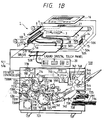
- Fig. 1A is a block diagram of an entire image processing apparatus (copying machine) constituting a first embodiment of the present invention.
- a CCD 100 for reading the image in each color component of red, green and blue; an A/D converter 101 for converting the analog signal into a digital signal; a color masking unit 102 for color correction; an UCR unit 103 for undercolor removal; a timing circuit 104; a selector 105 functioning on the signal obtained by a block process unit 112; a gradation correction unit 106 for correcting the gradation according for example to the characteristics of printer; a filter unit 107 for smoothing or edge enhancement of the image data; a full-color laser beam printer (LBP) 108 for printing an image with toners of yellow, magenta, cyan and black colors; AND gates 109, 110; a binary digitizing circuit 111 for obtaining binary signals from A/D converted data; a block processing unit 112; an exclusive OR gate 113; an OR gate 114; an area generation circuit 115 for generating plural area signals and enable signals; a digitizer 116 for area designation from the outside; a serial
- Fig. 1B shows an example of the internal structure of the digital color image processing system of the present embodiment, consisting of a digital color image reading unit 1 (hereinafter called color reader) in the upper part, and a digital color image printing unit 108 (hereinafter called color printer) in the lower part.
- Said color reader 1 reads the original color image information in respective colors by color separating means and a photoelectric converting device such as CCD 100, and converts said information into an electric digital image signal.
- the color printer 108 is an electrophotographic laser beam color printer for reproducing the color image by respective colors according to said digital image signal and transferring said image in digital dots plural times to a recording sheet.
- an original 3 There are shown an original 3; a platen glass 4 for supporting said original; and a rod lens array 5 concentrating the light, reflected from the original illuminated by a halogen lamp 10, onto a same-size full-color image sensor 100.
- the components 5, 6, 7 and 10 are integrated as a scanning unit 11 for effecting the scanning motion in a direction A1.
- the color-separated image signal, obtained for each line by said scanning motion is amplified to a predetermined voltage level by an amplifying circuit 7, and is supplied through a signal line 501 to a video processing unit for signal processing, as will be explained later.
- a concentric cable 501 is used for ensuring faithful signal transmission.
- a signal line 502 is used for supplying the driving pulses for the full-color image sensor 100, generated in the video processing unit 12.
- White and black plates 8, 9 are used for generating predetermined signal levels when illuminated by the halogen lamp 10, thereby correcting the white and black levels of the video signal.
- a control unit 13 incorporating a microcomputer executes all the control operations of the color reader 1, including the display and key input of a control panel 3150 through a bus 508, control of the video processing unit 12, detection of the scanning unit 11 by position sensors S1, S2 through signal lines 509, 510, control of a stepping motor driving circuit for a stepping motor 14 used for driving the scanning unit 11 through a signal line 503, on/off and intensity control of the halogen lamp 10 through a lamp driver and a signal line 504, control of digitizer 116, internal keys and display unit through a signal line 505.
- the color image signal read by the scanning unit 11 in the original scanning operation is supplied, through the amplifying circuit 7 and the signal line 501, to the video processing unit 12 for various processes to be explained later, and is further supplied to the printer unit 108 through an interface circuit 56.
- a scanner 711 is provided with a laser unit for converting the image signal from the color reader 1 into optical signal, a polygon mirror 712 (for example octagonal), a motor (not shown) for rotating said mirror 712, and an f- ⁇ (imaging) lens 713. There are further shown a mirror 714 for deflecting the laser beam, and a photosensitive drum 715. The laser beam emitted from the laser unit is reflected by the polygon mirror 712, then is guided by the lens 713 and the mirror 714, and performs raster scanning on the surface of the photosensitive drum 715, thereby forming a latent image corresponding to the original image.
- a primary charger 711 Around the photosensitive drum 715 there are provided a primary charger 711, a flush exposure lamp 718, a cleaner unit 723 for recovering the toner remaining in the image transfer, and a pre-transfer charger 724.
- a developing unit 726 for developing the electrostatic latent image formed on the photosensitive drum 715 by the laser beam is provided with developing sleeves 731Y, 731M, 731C, 731Bk for effecting the image development in direct contact with the photosensitive drum 715, toner hoppers 730Y, 730M, 730C, 730Bk for holding toners, and screws 732 for transferring the toners. These members are positioned about a rotary shaft P of the developing unit. For example, for forming a yellow toner image, the image development is conducted in the illustrated position with yellow toner.
- the developing unit 726 is rotated about the shaft P until the developing sleeve 731M of the magenta developing unit comes into contact with the photosensitive drum 715.
- the image development with cyan or black toner is conducted also in a similar manner.
- a transfer drum 716 is provided for transferring the toner image, formed on the photosensitive drum 715, onto a sheet.
- sheet cassettes 735, 376 containing recording sheets; sheet feeding rollers 737, 738 for feeding sheets from said cassettes 735, 736; and timing rollers 739, 740, 741 for adjusting, the timing of sheet feeding and transportation.
- the sheet transported by these components is guided by a sheet guide 749, and, with the leading end being gripped by a gripper to be explained later, is wound around the transfer drum 716, thus entering an image forming process.
- drum rotating motor 550 for rotating the photosensitive drum 715 and the transfer drum 176 in synchronization; a separating finger 750 for separating the sheet from the transfer drum 716 after the completion of the image forming process; a conveyor belt 742 for transporting the separated sheet; and an image fixing unit 743 for fixing the image of the sheet transported by the conveyor belt 742, including a pair of heated pressure rollers 744, 745.
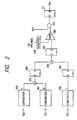
- Fig. 2 shows a conventional example of the binary digitizing circuit 111 mentioned above.
- Fig. 2 there are shown color component data 122-1 - 122-3 of R, G and B colors after A/D conversion; converters 200 - 202 for conversion into data of yellow (Y), magenta (M) and cyan (C) colors; adders 203, 206; D-flip-flops 204, 205, 207, 211 for timing adjustment; a register 208; a comparator 209; and an AND gate 210.
- the signals 122-1 - 122-3 are respectively converted into Y, M and C signals. Then Y + M + C is determined by the adders 203, 206, and is compared, in the comparator 209, with the data set in the register 208 by the CPU 118 through the CPU bus 121.
- the AND gate 210 functions as an enable gate, releasing a binary digitized signal according to an enable signal 123 from the area generation circuit 115. Said binary digitizing circuit 111 generates an area signal which is "1" in the position of character as shown in Fig. 7C.
- Fig. 3 shows the binary digitizing circuit 111 employed in the present invention. Said circuit is capable of noise elimination by a block processing.
- FIFO first-in-first-out
- the circuit down to the comparator 209 generates the binary digitized signal by a process same as in the circuit shown in Fig. 2.
- the present circuit is characterized by the ensuing process.
- Fig. 7B there is considered a 3 x 3 pixel block around the pixel to be contemplated, and, if 8 pixels a 13 , a 12 , a 11 , a 23 , a 21 , a 33 , a 32 , a 31 neighboring to the contemplated pixel are all 0, said pixel is digitized as 0 regardless whether the data a 22 thereof is 1 or 0. In this manner an isolated point in the image is detected, and is excluded from the block processing (contoured character process).
- Such process eliminates the noises ns1, ns2, ... in the original image as shown in Fig. 7A, thus providing noise-free digitized signal. Consequently, in the ensuing contoured character process, there can be prevented the deterioration of the image resulting from contouring on the noises.
- the above-explained circuit functions in the following manner.
- the binary data obtained from the comparator 209 are supplied to the FIFO register 301 and the D-flip-flop 302.
- the FIFO register 301 supplies the D-flip-flop 305 with binary data after the delay of a line (data of contemplated line), and the D-flip-flop 308 with binary data after the delay of two lines.
- the data of eight pixels excluding the contemplated pixel are supplied to the OR gate 311, which supplies the AND gate 132 with a signal "1" if at least one of said eight pixels is not “0", or with a signal "0” if all of said eight pixels are "0". Consequently, if all the eight pixels are "0", a signal "0" is supplied to the DF/F 313 regardless of the value of the contemplated pixel.
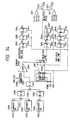
- Fig. 4 shows the structure of the block processing unit 112.
- DF/F's 301 - 325 for timing control arranged in a 5 x 5 matrix; a FIFO register 326 for the delay of a line; OR gates 401, 402; a register 403; a selector 404; and DF/F's 405, 406 for timing control.
- a binary signal 124 obtained from the binary digitizing circuit 111 is supplied at first to the FIFO register 326 and the DF/F 301, and the binary data of 5 x 5 pixel block are extracted in the block processing unit in a similar manner as in the circuit shown in Fig. 3.
- the data of 3 x 3 pixels around d 22 are supplied to the OR gate 401, and those of 5 x 5 pixels around d 22 are supplied to the OR gate 402.
- the OR gate 401 releases a signal "1" when at least one of 9 input pixels is “1”, while the OR gate 402 releases a signal "1" when at least one of 25 input pixels is “1".
- the register 403 memorizes the command from the CPU 118 and switches the selector 404 either to a side A or to a side B. Since the side A and B respectively select the 3 x 3 matrix or 5 x 5 matrix, the side B provides a thicker contoured character. Thus a discrimination signal 125 is obtained through the DF/F 405 for timing control.
- the 3 x 3 matrix or 5 x 5 matrix is selected by the CPU 118 through the selector 404, and the operator can arbitrarily select a thin contoured character or a thick contoured character.
- the signal of the contemplated pixel d 22 is obtained as a through data 126, through the DF/F 406 for timing control.
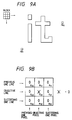
- Fig. 5 illustrates the block processing, indicating that a 3 x 3 block processing on an image indicated by a solid line provides a broken-lined image. More specifically, said processing corresponds to the formation, from binary signals as shown in Fig. 7C, of an area signal representing a thicker character as shown in Fig. 7D.
- Figs. 6A to 6C illustrate the binary data 124 in the 3 x 3 block, corresponding to an edge portion of a character.
- the 3 x 3 matrix is selected in the block processing unit 112.
- the area signal 125 is "0”
- the input signals to the gate 114 are both "0”
- a 3 0.
- the outputs of the AND gates 109, 110 or the input signals S 1 , S 2 of the selector 105 are "0".
- the above-mentioned selector 105 selects the terminal A, whereby the image data released from the under-color removal unit 103 are directly supplied to the gradation correction unit 106.
- the selector 105 selects B in the character area and C in the edge area (hatched area in Fig. 7B) of the character, so that the color can be arbitrarily selected by the CPU 118 both in the character area and the edge area.
- the present embodiment is capable of prohibiting the contoured character process on noises of the image, in case such noises are detected.
- the present embodiment employs 3 x 3 and 5 x 5 matrixes as the block pixel areas, but there may be arbitrarily employed larger or smaller matrixes. Also there may be employed an arbitrary number of matrixes, instead of two matrixes in the present embodiment. Furthermore it is also possible to render the size of the matrix freely variable. The thickness of the contoured character can be arbitrarily changed by these factors.
- the contemplated pixel is digitized as "0" in case all the surrounding pixels are "0", but it is also possible to identify a noise by counting the number of 0 pixels in the surrounding pixels and if said number exceeds a certain threshold value. An appropriate noise detection can be achieved by suitable selection of said threshold value.
- a contoured character is obtained by coloring the edge of the character, but it is also possible to form a pattern such as hatching or dots in the edge portion, or to form a colored pattern.
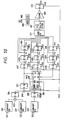
- FIG. 10 a block diagram shown in Fig. 10, for explaining a second embodiment of the present invention, which is featured by the block processing prior to the binary digitizing.
- the circuit shown in Fig. 10 is different from that shown in Fig. 3, in that an adder 411 and a 1/9 multiplier 412 are placed after the block processing and in front of the comparator 209 for binary digitizing. More specifically, the average value within a block is obtained by adding nine data a 11 - a 33 , and multiplying 1/9.
- the density of the isolated (ns1, ns2) as shown in Fig. 8A or 9A is considerably reduced, to a level below the value set in the register 208. Consequently the noises are eliminated, and the contoured character process can be applied only to the desired characters.
- the present embodiment allows, in the presence of noises, to eliminate such noises at the digitizing, thereby preventing the contoured character process on such noises.
- the present embodiment is capable of precise noise elimination, since the correlation within the block is taken into consideration at the binary digitizing, as the binary digitizing is conducted utilizing the average value within the block.
- Fig. 11 is a block diagram of a third embodiment of the present invention, in which the block processing is conducted prior to the binary digitizing.
- the present embodiment is featured by the use of a center value obtained by a median filter, instead of the average value in the second embodiment.
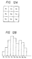
- a median filter selects, for example in a 3 x 3 block as shown in Fig. 12A with density distribution as shown in Fig. 12B, the center value counted in descending order of density, namely the value of a 32 , as the value of the contemplated pixel a 22 .
- the difference from the embodiment shown in Fig. 10 lies in a fact that the binary digitizing is based on the center, obtained by a 3 x 3 median filter 511, as the data of the contemplated pixel.
- Fig. 13 is a block diagram of a fourth embodiment of the present invention.
- the image processing apparatus of the present embodiment is provided with a CPU 2118 connected to a CPU bus 2121; a ROM 2119 storing for example an image processing program to be explained later; a RAM 2120 serving as an auxiliary memory; a bit map memory 2130; a selector 2142; a magnification varying unit (1) 2142; a CCD line sensor 2100; an A/D converter 2101; a color masking unit 2102; an undercolor removal unit 2103; a timing circuit 2104; a binary digitizing circuit 2111 for effecting binary digitizing on the A/D converted data; a block processing unit 2112; an area generation circuit 2115 for generating plural area signals and enable signals; a selector 2105 functioning based on a signal obtained from the block processing unit 2112; a gradation correction unit 2140; a magnification varying unit (2) 2106; a filter unit 2107; and a color laser beam printer 2108.
- Fig. 14 shows the binary digitizing circuit employed in the present embodiment.
- the R, G and B data 2122-1 - 2122-3 after A/D conversion are converted into Y, M and C data by converters 2200 - 2202.
- adders 2203, 2206 determine a signal Y + M + C, which is binary digitized by comparison, in a comparator 2209, with a value set by the CPU 2118 in a register 2208. In this manner there is generated an area signal which assumes a value "1" only in the position of character as shown in Fig. 7C.
- the binary digitized data are subjected to noise elimination in a succeeding process as will be explained in the following.
- a noise elimination circuit is composed of a comparator 2209; a FIFO register 2301 for line delay; DF/F's 2302 - 2310, 2313; an 8-input NOR gate 2311; an 8-input NAND gate 2311'; AND gates 2312, 2312'; and a DF/F 2313.
- the contemplated pixel is digitized as "0" regardless of its value, if the surrounding eight pixels a 13 - a 11 , a 23 , a 21 , a 33 - a 31 are all "0", and the digitized output is released as a binary signal 124.
- the NAND gate 2311′ releases "1" if the eight pixels a 13 - a 11 , a 23 , a 21 , a 33 - a 31 around the contemplated pixel a 22 are all "0".
- the AND gate 2312′ detects the isolated point (noise), and the detected noise is released as a binary signal 2124′.
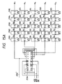
- Figs. 15A - 15D illustrate the details of the block processing unit 112.
- a FIFO register 2326 and DF/F's 2301 - 2325 constitute a circuit for forming a block of 5 x 5 pixels. More specifically, the FIFO memory 2326 generates a data block of synchronized five lines, and the DF/F's 2301 - 2325 generate a data block of 5 pixels.
- Fig. 15B shows a circuit for effecting a block processing on the pixel block formed in the circuit shown in Fig. 15A, and said block processing circuit is composed of OR gates 2401, 2402; a selector 2404 for selecting the input signal from the gate 2401 or 2402 according to the data set by the CPU 2121 in a register 2403; and a DF/F 2405 for timing control.
- Said selector 2404 for selecting the block size allows to vary the width of the contour of the contoured character.
- the OR gate 2401 releases an output signal "1" if a 3 x 3 pixel block defined around the contemplated pixel a 22 contains at least a signal "1", while the OR gate 2402 releases an output signal "1" if a 5 x 5 pixel block defined around the contemplated pixel d 22 contains at least a signal "1".
- One of said output signals is selected by the selector 2404 and is released as a signal 2125.
- Fig. 15C shows a DF/F 2406 which releases the through data of the contemplated pixel d 22 as a timing control signal 2126, for the signal 2124 entered into the block processing circuit.
- Fig. 15D shows DF/F's 2407, 2408, 2409 for releasing the signal 2124′ indicating a noise pixel, as a signal 2126′ after timing control.
- the binary digitized signal 2124 is supplied to the selector 2141 and the AND gate 2131.
- the binary digitized signal 2124 is recorded in the bit map memory 2130.
- the data 2143 read from the bit map memory 2130 in response to the enable signal EN from the CPU bus 2121 are supplied to the selector 2141. Consequently the selector 2141 selects either the signal 2124 directly from the binary digitizing circuit, or the signal 2143 once stored in the bit map memory 2130, according to the control signal from the CPU bus 2121.
- the output of said selector 2141 is subjected to a variation in the magnification, in the succeeding magnification varying circuit (1) 2142, according to the magnification set through the CPU bus 2121, and said variation can be achieved by a known process such as data skipping or data interpolation.
- the signal 2124 ⁇ after the variation of magnification and the noise signal 2124′ are supplied then to the block processing circuit 2112, which executes the above-explained process and releases a frame signal (enlarged character signal) 2125, a character signal 2126, and a timing-controlled noise signal 2126′.
- the signals 2125, 2126 are supplied to an exclusive logic sum circuit 2113 which supplies the succeeding AND gate with a signal "1" only in case the character signal and the frame signal are both "1" or both "0".
- the noise signal 2126′ is supplied to an AND gate 2154.
- Fig. 17 shows a truth table with para-a 1 , a 2 , a 3 , s 1 and s 2 relating to the selector 2105, when the signals 2150, 2151, 2152 from the area generation circuit and the signal 2153 from the CPU bus are turned on.
- the character area and the frame area are respectively represented by the signals a 1 and a 3 .
- the gates 2109, 2110, 2133, 1234 select the selector A for a background area, B for a frame area, C for a character area and D for a noise, and the noise area can be matched to the background color for example by setting, in a register of thus selected D, the average value of the background color of a 3 x 3 pixel block defined around said noise pixel, as shown in Fig. 18. This can be achieved by fetching the image data from the undercolor removal unit 2103 into the CPU 2118 through the CPU bus 2121, calculating the average value in a predetermined block, and setting the result of said calculation in the register D of the selector 2105 through the CPU bus 2121.
- noise pixels even when they are filled with white, or zero color-separated data, instead of the background color, are inconspicuous if they are small in size, so that it is conceivable to set zero data in the register D.
- the selector 2105 selects the original data A.
- data C arbitrarily set by the CPU 2118.
- Said data can designate any arbitrary color, through the instruction from the CPU 2118.
- the data B and C are selected respectively in the character area and the hatched area, so that the operator can arbitrarily select colors in these areas.
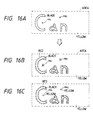
- the dots ns1, ns2 are regarded as noises, and do not appear in the output as the digitized signal 2124 becomes zero.
- the contoured character process applied to the image shown in Fig. 16A provides an output shown in Fig. 16C, in which the noises are matched to the background color and the contoured character process is applied only to the desired areas.
- the image synthesis is conducted by switching the selector 2105 according to the area signal 2152. The process of generating the contoured characters will not be explained as it is same as explained before.
- the image synthesis of the data of the bit map memory and the data of an original image with a change in magnification is achieved by applying a magnification change, for said original image, by data skipping or interpolation by the magnification varying unit (2) 2140 in the main scanning direction and by speed control of the scanning operation in the sub scanning direction.
- magnification change for the characters to be synthesized is conducted by the magnification varying unit (1) 2142 both in the main and sub scanning directions.
- the characters and another image can be independently varied in magnification, and the noise elimination can be conducted in the original sized image, regardless of the desired magnification.
- the present embodiment allows to eliminate noises from the image, by the use of block processing means (means for conducting a process utilizing a contemplated pixel and surrounding pixels) before or after the binary digitizing.
- the noise elimination can be conducted on the original-sized image by the use of means for noise elimination prior to the change in image magnification.
- the present embodiment has an advantage of achieving highly precise image processing with a compact circuit structure, in which the precision of noise elimination is not affected by the magnification varying process, by (1) replacing the area identified as noise with the background color in the binary digitizing process, and (2) effecting the noise elimination prior to the variation of image magnification at the character synthesis utilizing the result of binary digitizing.
- the present invention allows to reproduce the image of high quality with a simple structure and without the influence of noises.
- an embodiment of the present invention capable of providing, in real time, an output image in which at least a part of the input image data and a peripheral area thereof are colored in arbitrary colors in plural areas and in which the widths of said peripheral areas are independently variable, by employing means for binary digitizing the input image data and means for magnifying the area obtained by said binary digitizing means (with plural sizes and with plural area signals).
- Fig. 19 is a block diagram of the present embodiment, wherein provided are a CPU 3119 connected to a CPU bus 3121; a ROM 3119 storing programs etc.; a RAM 3120 serving as an auxiliary memory; an operation unit 3150 for various operations such as mode setting or color designation; a CCD line sensor 3100; an A/D converter 3101; a color masking unit 3102; an undercolor removal unit 3103; a timing circuit 3104; a binary digitizing circuit 3111 for effecting the binary digitization on the A/D converted data; a bit map memory 3130; an AND gate 3131; a block processing unit 3112; an area generation circuit 3115 for generating plural area signals and enable signals; a selector 3105 functioning according to the signal obtained by block processing; a gradation correction unit 3106; a filter unit 3107; a color laser beam printer 3108; an exclusive logic sum circuit 3111; an OR gate 3114; and AND gates 3109, 3110.
- the binary digitizing circuit in Fig. 19 is same as that shown in Fig. 2, and will not, therefore, be explained.
- Fig. 20 is a block diagram of the block processing unit 3112, for generating a block of 5 x 5 pixels, around a pixel d 22 .
- a FIFO memory 3326 generates a data block five synchronized lines, and DF/F's 3301 - 3325 generate a data block of 5 pixels.
- Fig. 20B shows a part including OR gates 3401, 3402 for effecting the actual block processing, and another part for releasing the through data.
- the OR gates releases a signal "1" if a 3 x 3 block defined around the pixel d 22 contains at least a signal "1”, while the OR gate 3402 releases a signal "1” if a 5 x 5 block defined around the pixel d 22 contains at least a signal "1”, and said output signals are selected and released as a signal 3125 by the selector 3404, in response to an area signal 3200 which is supplied through the CPU bus 3121 by an instruction from the operation unit 3150. It is therefore possible to vary the width of line on real-time basis, and to designate peripheral areas of different widths for plural areas.
- the selector 3105 selects the original image data A in said character area.
- the hatched area there are selected arbitrary data C set by the CPU 3118.
- the output image as shown in Fig. 7B can be obtained by so setting the data C in said register as to give red color to the hatched area.
- the process of generating the contoured characters will not be explained as it is same as explained before.
- the colors Y, M, C and Bk can be regulated or set in percentage (%) on a liquid crystal touch panel 1109 of the operation unit 3150.
- each color density is represented by 8 bits, or values from 00 to 255, so that a variation 1% corresponds to 2.55 in digital value.
- the actually set values are represented by (2.55y, 2.55m, 2.55c, 2.55k), and rounded integers are actually stored in the RAM 3120 by the CPU 3118.
- a variation by ⁇ % a value obtained by addition of 2.55 ⁇ in case of density increase or by subtraction of 2.55 ⁇ in case of density decrease can be stored in the RAM 3120.
- the color of the character and that of the contour can be arbitrarily selected.
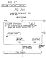
- the liquid crystal display unit 1109 In response to the depression of a character synthesis key 1114 of the operation unit, the liquid crystal display unit 1109 provides a display as shown in P020.
- Said display unit 1109 is composed of a touch panel display, which is capable of providing a display and of key inputs by actuating keys displayed thereon.
- a character original to be synthesized is placed on the platen glass and a key 1020 is depressed, whereby conducted are the reading of said character original, binary digitizing and storage of the image information in the bit map memory 3130.
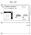
- the image area to be memorized can be designated by depressing a touch key 1021 in the display P020 to obtain a display P021, placing said character original on the digitizer 58, and designating a desired area by two points thereof, with the pointer pen of said digitizer.
- the display changes to a state P022, in which touch keys 1023, 1024 are used to select a trimming operation for reading the image inside the designated area, or a masking operation for reading the image outside said area.
- Some originals may contain characters which are difficult to extract in the binary digitizing, for example yellowish characters.
- the binary digitization can be suitably conducted according to the color and thickness of the original characters.
- Such change in the slice level in a designated area allows to achieve satisfactory binary digitizing for all the characters, for example in case an original of black characters contains yellow characters, by selecting suitable different slice level for such black and yellow characters.
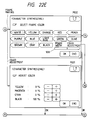
- the display unit 1109 shifts to a state P024 shown in Fig. 22.
- a touch key 1027 in the display is depressed to obtain a state P025, in which a character color to be synthesized is selected from the displayed colors.
- the character color can be selected, as shown in Fig. 22, from white, yellow, orange, red, pink, purple, blue, light blue, green, yellow-green, brown, gray and black.
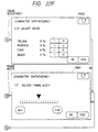
- a touch key 1030 is depressed in the state P025, the display is changed to a state P026 for color regulation, in which any desired color can be obtained by increasing or decreasing the yellow, magenta, cyan and black colors with respective or or key by a pitch of 1% as explained above.
- the designated color value is set by the CPU 3118 as the data B in the register of the selector 3105, through the CPU bus 3121.
- a touch key 1029 is depressed to obtain a display P027 in which an area is designated with the digitizer 3116. Then, in a display P030, the character color is selected in the same manner as explained above. If the area designated in this step is same as that designated previously area key and an OK key are depressed in succession in the display P029, whereby the repeated area designation can be dispensed with.
- a touch key 1031 in the display P030 is depressed to a display P032, in which the contour color is selected. In this case the color regulation is also possible in a display P033 as explained above.
- the width of the contour can be regulated in a display P041 obtained by a touch key 1033. The width of the contour can be varied by changing the size of the block processing as explained before.
- the display is shifted to a state P026 by the touch key 1130, for enabling the adjustment of the selected color.
- the designation of color may also be achieved by selecting the position of a desired color of the original placed on the platen glass with the digitizer 3116, and reading said color with the CCD 3100 in a pre-scanning operation.
- the present embodiment enables the contoured character processes with different colors in plural areas.
- the character and the contour can be converted into desired colors, which can be defined by yellow, magenta, cyan and black with a pitch of 1%.
- said color values may be entered by numeral keys 1115 (Fig. 23) instead of the touch keys. Said color values may be roughly defined or finely defined.
- the width of the contour can be arbitrarily varied, by changing the block size of the above-explained block processing.
- the width of contour in the present embodiment is selected by a 3 x 3 block or a 5 x 5 block
- the size of block is not limited to such sizes. It is also possible to select said size manually, or automatically according for example to the size of character.
- area to be designated is not limited to rectangular area.
- the image editing such as contoured character process can be realized simply and on real-time basis, by a simple hardware structure consisting of binary digitizing of input image data and block processing, thus providing wide applications particularly in various designs.
- image data may be entered from an electronic still camera, a video camera or a computer through an interface, instead of the CCD.
- contoured character process of the present invention is applicable not only to a still image but also to a moving image.
Landscapes
- Engineering & Computer Science (AREA)
- Physics & Mathematics (AREA)
- General Physics & Mathematics (AREA)
- Theoretical Computer Science (AREA)
- Computer Vision & Pattern Recognition (AREA)
- Multimedia (AREA)
- Signal Processing (AREA)
- Facsimile Image Signal Circuits (AREA)
- Image Processing (AREA)
Claims (10)
- Appareil de traitement d'image comprenant un moyen (100, 3100) pour introduire des données représentant une image;
un moyen (112, 3112) pour extraire une partie de bord de ladite image et générer des données binaires représentant la partie de bord, et un moyen (301-312) pour supprimer, des données binaires, tout point isolé entouré par une pluralité de pixels ayant chacun une couleur de fond, et caractérisé en ce qu'il est utilisé un moyen sélecteur (105, 3105) pour effectuer une sélection, en fonction des données binaires représentant une partie de bord, entre des données d'image d'un original correspondant aux données d'image d'entrée qui sont appliquées à une entrée dudit sélecteur, ou des données de couleurs préétablies qui sont fournies à une autre entrée dudit sélecteur, ledit sélecteur effectuant une sélection entre les deux séries de données en parallèle avec le moyen pour extraire une partie de bord, de manière à colorer la partie de bord. - Appareil selon la revendication 1, dans lequel ledit moyen de suppression supprime le point isolé par une opération logique sur les données binaires générées par ledit moyen d'extraction.
- Appareil selon la revendication 1, dans lequel ledit moyen de suppression supprime le point isolé des données binaires, en supprimant le point isolé des données d'image introduites par ledit moyen d'entrée.
- Appareil selon les revendications 1 à 3, comprenant en outre un moyen (104, 3104) de réglage de synchronisation pour régler la synchronisation de sortie des données dudit moyen d'entrée et dudit moyen d'extraction.
- Appareil selon l'une quelconque des revendications précédentes, dans lequel les données d'image d'entrée comprennent une pluralité de données de composante de couleur.
- Appareil selon la revendication 5, comprenant en outre un moyen de correction (102, 3102) pour effectuer une correction de couleur sur les données d'image d'entrée.
- Appareil selon l'une quelconque des revendications précédentes, comprenant en outre un moyen (106, 3106) de correction de gradation pour effectuer une correction de gradation sur les données d'image délivrées par ledit moyen de sélection.
- Appareil selon l'une quelconque des revendications précédentes, comprenant en outre un moyen (108, 3108) de formation d'image pour former une image sur un support.
- Appareil selon la revendication 8, dans lequel ledit moyen de formation d'image est une imprimante à faisceau laser.
- Procédé de traitement d'image comprenant:l'introduction de données d'image;l'extraction d'une partie de bord de l'image représentée par les données d'image d'entrée et la génération de données binaires représentant la partie de bord; etla suppression, des données binaires, de chaque point isolé qui est entouré par une pluralité de pixels ayant la même couleur de fond, et caractérisé en ce qu'il comprend en outrela sélection, en fonction des données binaires qui représentent une partie de bord extraite, soit de données d'image d'un original correspondant aux données d'image d'entrée, soit de données de couleurs prédéterminées;ladite sélection et ladite extraction étant effectuées en parallèle, de manière à colorer la partie de bord.
Applications Claiming Priority (6)
| Application Number | Priority Date | Filing Date | Title |
|---|---|---|---|
| JP97722/89 | 1989-04-18 | ||
| JP1097722A JP2832027B2 (ja) | 1989-04-18 | 1989-04-18 | 画像処理装置 |
| JP117014/89 | 1989-05-10 | ||
| JP117015/89 | 1989-05-10 | ||
| JP1117014A JPH02294877A (ja) | 1989-05-10 | 1989-05-10 | 画像処理装置 |
| JP1117015A JPH02294878A (ja) | 1989-05-10 | 1989-05-10 | 画像処理装置 |
Publications (2)
| Publication Number | Publication Date |
|---|---|
| EP0398501A1 EP0398501A1 (fr) | 1990-11-22 |
| EP0398501B1 true EP0398501B1 (fr) | 1996-09-04 |
Family
ID=27308480
Family Applications (1)
| Application Number | Title | Priority Date | Filing Date |
|---|---|---|---|
| EP90304090A Expired - Lifetime EP0398501B1 (fr) | 1989-04-18 | 1990-04-17 | Appareil de traitement d'images |
Country Status (3)
| Country | Link |
|---|---|
| US (1) | US5485529A (fr) |
| EP (1) | EP0398501B1 (fr) |
| DE (1) | DE69028345T2 (fr) |
Families Citing this family (8)
| Publication number | Priority date | Publication date | Assignee | Title |
|---|---|---|---|---|
| EP0447541B1 (fr) * | 1989-10-10 | 1998-06-10 | Unisys Corporation | Systeme et methode de traitement d'images |
| JP3068628B2 (ja) * | 1990-03-22 | 2000-07-24 | キヤノン株式会社 | 画像処理装置およびその方法 |
| JPH07264392A (ja) * | 1994-02-04 | 1995-10-13 | Canon Inc | 画像編集装置、画像処理装置及び画像処理方法 |
| JP3554034B2 (ja) * | 1994-09-02 | 2004-08-11 | キヤノン株式会社 | カラー印刷装置及びその方法 |
| US5974195A (en) * | 1994-10-14 | 1999-10-26 | Canon Kabushiki Kaisha | Image processing apparatus and method |
| JPH0951489A (ja) * | 1995-08-04 | 1997-02-18 | Sony Corp | データ符号化/復号化方法および装置 |
| US5956421A (en) * | 1996-02-28 | 1999-09-21 | Canon Kabushiki Kaisha | Image processing method and apparatus for determining a binarization threshold value used for binarizing a multi-valued image and performing binarization processing |
| JP2004077841A (ja) * | 2002-08-19 | 2004-03-11 | Fuji Xerox Co Ltd | 画像形成処理方法及び画像形成処理装置 |
Family Cites Families (8)
| Publication number | Priority date | Publication date | Assignee | Title |
|---|---|---|---|---|
| US4415920A (en) * | 1980-09-19 | 1983-11-15 | Canon Kabushiki Kaisha | Image signal processing unit |
| DE3220298A1 (de) * | 1981-06-01 | 1982-12-16 | Canon K.K., Tokyo | Farbbild-lesegeraet |
| US4601002A (en) * | 1983-01-06 | 1986-07-15 | The United States Army Corps Of Engineers As Represented By The Secretary Of The Army | Digital technique for constructing variable width lines |
| DE3583040D1 (de) * | 1985-12-17 | 1991-07-04 | Ibm | Bild-vorverarbeitungsverfahren zur rauschentfernung. |
| US4769849A (en) * | 1985-12-19 | 1988-09-06 | The Palantir Corporation | Method and apparatus for separating overlapping patterns |
| JPS62216478A (ja) * | 1986-03-17 | 1987-09-24 | Dainippon Screen Mfg Co Ltd | 網ふせ装置 |
| JPH0693741B2 (ja) * | 1988-01-14 | 1994-11-16 | 大日本スクリーン製造株式会社 | 網伏せにおける画像整形方法 |
| US4991022A (en) * | 1989-04-20 | 1991-02-05 | Rca Licensing Corporation | Apparatus and a method for automatically centering a video zoom and pan display |
-
1990
- 1990-04-17 EP EP90304090A patent/EP0398501B1/fr not_active Expired - Lifetime
- 1990-04-17 DE DE69028345T patent/DE69028345T2/de not_active Expired - Fee Related
-
1994
- 1994-05-17 US US08/245,079 patent/US5485529A/en not_active Expired - Lifetime
Also Published As
| Publication number | Publication date |
|---|---|
| DE69028345T2 (de) | 1997-01-23 |
| EP0398501A1 (fr) | 1990-11-22 |
| US5485529A (en) | 1996-01-16 |
| DE69028345D1 (de) | 1996-10-10 |
Similar Documents
| Publication | Publication Date | Title |
|---|---|---|
| EP0899685B1 (fr) | Appareil et procédé pour discriminer plusieurs fois des champs d'image dans un document original | |
| EP0588380B1 (fr) | Appareil et procédé de traitement d'images | |
| EP1617646B1 (fr) | Appareil et procédé de traitement d'image | |
| EP0855830B1 (fr) | Différentiation de textes/lignes et de demi-teintes pour l'amélioration de la résolution des éléments d'image | |
| EP0881822B1 (fr) | Amélioration de la définition chromatique à partir de la luminance | |
| JPH0410765A (ja) | 画像処理装置 | |
| JPH05268457A (ja) | 多色マーカー編集装置 | |
| JP3317446B2 (ja) | 画像処理装置 | |
| EP0398501B1 (fr) | Appareil de traitement d'images | |
| US5930385A (en) | Apparatus and method for image conversion | |
| US8610957B2 (en) | Image processing apparatus, image processing method, and non-transitory computer-readable medium | |
| EP0350919B1 (fr) | Appareil de production d'images à couleurs | |
| US20070279660A1 (en) | Color image processing apparatus | |
| JP3618776B2 (ja) | 画像処理装置及び方法 | |
| US5757378A (en) | Color image processing apparatus | |
| JP3262360B2 (ja) | 画像処理装置及び画像処理方法 | |
| JP3245153B2 (ja) | 画像処理装置 | |
| JP3297452B2 (ja) | 画像処理装置及び画像処理方法 | |
| JP3003133B2 (ja) | イメージ外形線抽出装置 | |
| JP3729131B2 (ja) | 画像形成装置 | |
| JP3183788B2 (ja) | 網点領域判定装置 | |
| JP3079630B2 (ja) | 画像処理装置 | |
| JPH04342370A (ja) | 画像形成装置 | |
| JP2001144943A (ja) | 画像処理方法及び画像処理装置 | |
| JP2952023B2 (ja) | カラー画像処理装置 |
Legal Events
| Date | Code | Title | Description |
|---|---|---|---|
| PUAI | Public reference made under article 153(3) epc to a published international application that has entered the european phase |
Free format text: ORIGINAL CODE: 0009012 |
|
| AK | Designated contracting states |
Kind code of ref document: A1 Designated state(s): DE FR GB IT |
|
| 17P | Request for examination filed |
Effective date: 19901231 |
|
| 17Q | First examination report despatched |
Effective date: 19940804 |
|
| GRAH | Despatch of communication of intention to grant a patent |
Free format text: ORIGINAL CODE: EPIDOS IGRA |
|
| GRAH | Despatch of communication of intention to grant a patent |
Free format text: ORIGINAL CODE: EPIDOS IGRA |
|
| GRAA | (expected) grant |
Free format text: ORIGINAL CODE: 0009210 |
|
| AK | Designated contracting states |
Kind code of ref document: B1 Designated state(s): DE FR GB IT |
|
| REF | Corresponds to: |
Ref document number: 69028345 Country of ref document: DE Date of ref document: 19961010 |
|
| ET | Fr: translation filed | ||
| ET | Fr: translation filed | ||
| ITF | It: translation for a ep patent filed | ||
| PLBE | No opposition filed within time limit |
Free format text: ORIGINAL CODE: 0009261 |
|
| STAA | Information on the status of an ep patent application or granted ep patent |
Free format text: STATUS: NO OPPOSITION FILED WITHIN TIME LIMIT |
|
| 26N | No opposition filed | ||
| REG | Reference to a national code |
Ref country code: GB Ref legal event code: IF02 |
|
| PGFP | Annual fee paid to national office [announced via postgrant information from national office to epo] |
Ref country code: GB Payment date: 20060418 Year of fee payment: 17 |
|
| PGFP | Annual fee paid to national office [announced via postgrant information from national office to epo] |
Ref country code: FR Payment date: 20060426 Year of fee payment: 17 |
|
| PGFP | Annual fee paid to national office [announced via postgrant information from national office to epo] |
Ref country code: IT Payment date: 20060430 Year of fee payment: 17 |
|
| PGFP | Annual fee paid to national office [announced via postgrant information from national office to epo] |
Ref country code: DE Payment date: 20060621 Year of fee payment: 17 |
|
| GBPC | Gb: european patent ceased through non-payment of renewal fee |
Effective date: 20070417 |
|
| PG25 | Lapsed in a contracting state [announced via postgrant information from national office to epo] |
Ref country code: DE Free format text: LAPSE BECAUSE OF NON-PAYMENT OF DUE FEES Effective date: 20071101 |
|
| PG25 | Lapsed in a contracting state [announced via postgrant information from national office to epo] |
Ref country code: GB Free format text: LAPSE BECAUSE OF NON-PAYMENT OF DUE FEES Effective date: 20070417 |
|
| PG25 | Lapsed in a contracting state [announced via postgrant information from national office to epo] |
Ref country code: FR Free format text: LAPSE BECAUSE OF NON-PAYMENT OF DUE FEES Effective date: 20070430 |
|
| PG25 | Lapsed in a contracting state [announced via postgrant information from national office to epo] |
Ref country code: IT Free format text: LAPSE BECAUSE OF NON-PAYMENT OF DUE FEES Effective date: 20070417 |