EP0399191A1 - Méthode de fabrication d'un transistor auto-aligné avec source et drain légèrement dopé formés dans une tranchée - Google Patents
Méthode de fabrication d'un transistor auto-aligné avec source et drain légèrement dopé formés dans une tranchée Download PDFInfo
- Publication number
- EP0399191A1 EP0399191A1 EP90106685A EP90106685A EP0399191A1 EP 0399191 A1 EP0399191 A1 EP 0399191A1 EP 90106685 A EP90106685 A EP 90106685A EP 90106685 A EP90106685 A EP 90106685A EP 0399191 A1 EP0399191 A1 EP 0399191A1
- Authority
- EP
- European Patent Office
- Prior art keywords
- trench
- region
- well region
- doped
- lightly
- Prior art date
- Legal status (The legal status is an assumption and is not a legal conclusion. Google has not performed a legal analysis and makes no representation as to the accuracy of the status listed.)
- Granted
Links
Images



Classifications
-
- H—ELECTRICITY
- H10—SEMICONDUCTOR DEVICES; ELECTRIC SOLID-STATE DEVICES NOT OTHERWISE PROVIDED FOR
- H10B—ELECTRONIC MEMORY DEVICES
- H10B12/00—Dynamic random access memory [DRAM] devices
- H10B12/01—Manufacture or treatment
-
- H—ELECTRICITY
- H10—SEMICONDUCTOR DEVICES; ELECTRIC SOLID-STATE DEVICES NOT OTHERWISE PROVIDED FOR
- H10B—ELECTRONIC MEMORY DEVICES
- H10B12/00—Dynamic random access memory [DRAM] devices
- H10B12/30—DRAM devices comprising one-transistor - one-capacitor [1T-1C] memory cells
- H10B12/39—DRAM devices comprising one-transistor - one-capacitor [1T-1C] memory cells the capacitor and the transistor being in a same trench
-
- H—ELECTRICITY
- H10—SEMICONDUCTOR DEVICES; ELECTRIC SOLID-STATE DEVICES NOT OTHERWISE PROVIDED FOR
- H10D—INORGANIC ELECTRIC SEMICONDUCTOR DEVICES
- H10D30/00—Field-effect transistors [FET]
- H10D30/60—Insulated-gate field-effect transistors [IGFET]
- H10D30/601—Insulated-gate field-effect transistors [IGFET] having lightly-doped drain or source extensions, e.g. LDD IGFETs or DDD IGFETs
- H10D30/608—Insulated-gate field-effect transistors [IGFET] having lightly-doped drain or source extensions, e.g. LDD IGFETs or DDD IGFETs having non-planar bodies, e.g. having recessed gate electrodes
-
- H—ELECTRICITY
- H10—SEMICONDUCTOR DEVICES; ELECTRIC SOLID-STATE DEVICES NOT OTHERWISE PROVIDED FOR
- H10D—INORGANIC ELECTRIC SEMICONDUCTOR DEVICES
- H10D30/00—Field-effect transistors [FET]
- H10D30/60—Insulated-gate field-effect transistors [IGFET]
- H10D30/63—Vertical IGFETs
-
- H—ELECTRICITY
- H10—SEMICONDUCTOR DEVICES; ELECTRIC SOLID-STATE DEVICES NOT OTHERWISE PROVIDED FOR
- H10P—GENERIC PROCESSES OR APPARATUS FOR THE MANUFACTURE OR TREATMENT OF DEVICES COVERED BY CLASS H10
- H10P32/00—Diffusion of dopants within, into or out of wafers, substrates or parts of devices
- H10P32/10—Diffusion of dopants within, into or out of semiconductor bodies or layers
- H10P32/12—Diffusion of dopants within, into or out of semiconductor bodies or layers between a solid phase and a gaseous phase
- H10P32/1204—Diffusion of dopants within, into or out of semiconductor bodies or layers between a solid phase and a gaseous phase from a plasma phase
-
- H—ELECTRICITY
- H10—SEMICONDUCTOR DEVICES; ELECTRIC SOLID-STATE DEVICES NOT OTHERWISE PROVIDED FOR
- H10B—ELECTRONIC MEMORY DEVICES
- H10B20/00—Read-only memory [ROM] devices
Definitions
- the present invention relates to a vertical lightly-doped drain trench transistor for ROM and DRAM cells and to a method of fabricating the same.
- This surface is oxidized and photoresist masked conventionally to open regions for the slots which are ion milled or ODE etched to a given depth.
- P+ regions are established by the slots by ion implanting at an angle such that the entire depth of the slot is not doped but rather the doping is confined to a region within the double energy N implanted depth.
- Drive-in diffusion enlarges the P+ areas for the emitter and collector and oxidation fills the moat insulating regions around the active area.
- the oxide is stripped and the N region enhanced to N+ at the surface, with silox being deposited and opened for metal contacts to the N+ region for the base and the emitter and collector regions.
- the doping profile of the base region provides a potential barrier to minimize the flow of electrons toward the surface because the emitter electrons are channeled through the less heavily doped part of the base region to the collector.
- a shielding electrode is insulated between first and second gate electrode in a notch between laterally spaced source regions and channel regions joined by a common drift region around the bottom of the notch.
- the shielding electrode is ohmically connected to the substrate containing the common drift region to be at the same potential level thereof and within a single junction drop of a respective main electrode across the junction between the respective channel containing region and drift region.
- the steering diode function for referencing the shielding electrode is performed by junctions already present in the integrated structure, eliminating the need for discrete dedicated steering diodes.
- the shielding electrode prevents the electric field gradient toward the gate electrode on one side of the notch from inducing depletion in the drift region along the opposite side of the notch. This prevents unwanted inducement of conduction channels in the drift region during the OFF state of the FET.
- DRAM dynamic random access memory
- a trench is located in a p+ type substrate containing heavily doped N+ polysilicon.
- a composite film of SiO2/Si3N4/SiO2 is provided for the capacitor storage insulator.
- a thin layer of SiO2 is disposed over the polysilicon.
- a lightly doped p-type epi silicon layer is located over the substrate and SiO2 layer.
- the access transistor for the memory cell is located on top of the trench capacitor.
- An N+ doped material connects the source region of the transistor to the polysilicon inside the trench.
- a medium doped p-region on top of the trench surface may be provided in case there is any significant amount of leakage current along the trench surface.
- a DRAM cell and array of cells together with a method of fabrication, are disclosed wherein the cell includes one field effect transistor and one capacitor with both the transistor and the capacitor formed in a trench in a substrate.
- One capacitor plate and the transistor source are common and are formed in the lower portion of the trench sidewall.
- the transistor drain is formed in the upper portion of the trench sidewall to connect to a bit line on the substrate surface, and the channel is the vertical portion of the trench sidewall between the source and drain.
- a ground line runs past the transistor gate in the upper portion of the trench down into the lower portion of the trench to form the other capacitor plate.
- a semiconductor integrated circuit comprising semiconductor regions in the form of first and second protruding poles that are provided on a semiconductor layer formed on a semiconductor substrate or an insulating substrate, and that are opposed to each other with an insulating region sandwiched therebetween, a p-channel FET provided in the first semiconductor region, and an n-channel FET provided in the second semiconductor region.
- These FET's have source and drain regions on the upper and bottom portions of the semiconductor regions, and have gate electrodes on the sides of the semiconductor regions.
- the insulation region between the protruding pole-like semiconductor regions is further utilized as the gate electrode and the gate insulating film.
- the transistor has a gate insulating film adjacent to the capacitor and formed along a remaining portion of the sidewall surface of the trench, a gate electrode formed along the gate insulating film and a diffusion region formed in a major surface of the semiconductor substrate which is adjacent to the gate insulating film.
- the semiconductor memory device further has an isolation region between two adjacent ones of the memory cells along two adjacent ones of the bit or word lines. A method of manufacturing the semiconductor is also proposed.
- a DRAM cell and array of cells together with method of fabrication, are disclosed wherein the cell includes one field effect transistor and one storage capacitor with both the transistor and the capacitor formed in a trench in a substrate.
- the transistor source, channel, and drain and one capacitor plate are formed in a layer of material inserted into the trench and insulated from the substrate; the gate and other capacitor plate are formed in the substrate trench sidewall.
- bit lines on the substrate surface connect to the inserted layer, and word lines on the substrate surface are formed as diffusions in the substrate which also form the gate.
- the trenches and cells are formed in the crossings of bit lines and word lines; the bit lines and word lines form perpendicular sets of parallel lines.
- a vertical metal oxide semiconductor field effect transistor has a trench substantially vertically formed in a major surface of a semiconductor substrate, a first conductive layer formed in a predetermined region including a sidewall surface of the trench on a gate insulating film, lower and upper diffusion layers formed in the bottom of the trench and a surface layer of the semiconductor substrate, preferably a channel doped region formed in the semiconductor substrate between the upper and lower diffusion layers, and a second conductive layer formed in contact with the lower diffusion layer in the bottom of the trench and insulated from the first conductive layer so as to fill the trench.
- the first conductive layer serves as a gate electrode
- the diffusion layers serves as source/drain regions, respectively.
- DRAM three-dimensional dynamic random access memory
- an access transistor formed in monocrystalline silicon stacked on top of a trench capacitor.
- a fabrication method therefor is shown wherein the contact window for the source-to-trench connection is formed by self-aligned lateral epitaxial growth, followed by a contact-connection formation step using either a second epitaxial growth or a CVD refill and strapping process.
- the invention can be further applied to other device structures using the described principles, and more specifically to an inverter structure having the driver device stacked over the load-resistor as another example, which can be used as a basic building circuit unit for logic circuits and static-RAM cell.
- An object of the present invention is to provide an improved trench transistor including a lightly-doped drain/source (LDD) region.
- LDD lightly-doped drain/source
- Another object of the present invention is to provide an improved trench transistor structure to improve the electrical breakdown, short-channel effects and reliability.
- Another object of the present invention is to provide an improved fabrication process for providing a method to adjust (or control) the threshold voltage of trench transistor by using oblique angle ion implantation or electron cyclotron resonant (ECR) surface doping technique.
- ECR electron cyclotron resonant
- a further object of the present invention is to provide an improved performance for ROM and DRAM cells wherein the trench transistor with lightly-doped drain/source region is disposed in a cross-point at the crossing of a word line and bit line.
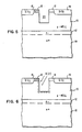
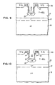
- a new fabrication process is described for a novel cross-point lightly-doped drain/source (LDD) trench transistor.
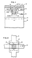
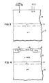
- the cross section of this new vertical transistor is shown in Fig. 1 together with a plan view of its schematic layout shown in Fig. 2.
- the trench transistor is built on the surface of a U-groove.
- the U-groove shallow trench transistor is designed to be disposed in a cross-point at the crossing of a wordline and a bit line of a memory.
- the layout of this transistor provides the advantages of ultra small size, high packing density, and faster performance.
- Fig. 12 The first example of an application of the LDD trench transistor to a cell array of a cross point ROM cell is shown in Fig. 12.
- the memory array for this system consists of 16,384 x 4 (64K) intersections, as indicated schematically in Fig. 13.
- This address code conversion to be performed by ROM is permanently programmed during the fabrication process by using a custom-designed BEOL mask so as to construct or omit a trench at each array intersection.
- Such an array is indicated in Fig. 13, which shows how the memory FETs are connected between word and bit lines. This arrangement is different from the conventional ROM array which is programmed at each bit line.
- n+ diffusion bit lines as interconnections leads to the advantage of reduced drain contact area. Furthermore, the source and drain are vertically isolated, so that there is no need for an isolation region in the cell array. A 3.6 ⁇ m2 cell is achievable using 0.7 ⁇ m technology. This corresponds to the cell size of 16 Mb ROMs.
- the LDD trench transistor of the present invention can also be used with DRAM cell arrays to improve the DRAM cell performance.
- new LDD access trench transistor can be incorporated into the prior art cross-point DRAM cells which are shown in Figs. 14 and 15, respectively, wherein the n-channel LDD trench transistor of the present invention is used instead of the conventional p-channel trench transistor.
- the thicker oxide over drain and source junctions are grown simultaneously.
- the coupling capacitances between the gate and drain junctions (or the wordline and bit line), and between the gate (WL) and storage node are reduced to a minimum. Hence the access performance of cross-point ROM and DRAM cells will be improved.
- the spacer defined lightly-doped drain (LDD) structure optimizes the vertical transistor.
- the transistor provides self-aligned source and drain junctions, improved short channel effect, improved punch-through characteristics, lower mobility degradation and reduced overlap capacitance with minimized source and drain incremental resistance.
- the topography of this new structure is flat after gate level; it can be easily enhanced by several additional levels of interconnecting metallurgy.
- the threshold voltage of vertical transistor can be adjusted by using oblique angle ion implantation technique, or electron cycletron resonant (ECR) surface doping technique.
Landscapes
- Engineering & Computer Science (AREA)
- Manufacturing & Machinery (AREA)
- Semiconductor Memories (AREA)
- Insulated Gate Type Field-Effect Transistor (AREA)
Applications Claiming Priority (2)
| Application Number | Priority Date | Filing Date | Title |
|---|---|---|---|
| US07/355,232 US4954854A (en) | 1989-05-22 | 1989-05-22 | Cross-point lightly-doped drain-source trench transistor and fabrication process therefor |
| US355232 | 2003-01-31 |
Publications (2)
| Publication Number | Publication Date |
|---|---|
| EP0399191A1 true EP0399191A1 (fr) | 1990-11-28 |
| EP0399191B1 EP0399191B1 (fr) | 1994-08-24 |
Family
ID=23396717
Family Applications (1)
| Application Number | Title | Priority Date | Filing Date |
|---|---|---|---|
| EP90106685A Expired - Lifetime EP0399191B1 (fr) | 1989-05-22 | 1990-04-06 | Méthode de fabrication d'un transistor auto-aligné avec source et drain légèrement dopé formés dans une tranchée |
Country Status (5)
| Country | Link |
|---|---|
| US (1) | US4954854A (fr) |
| EP (1) | EP0399191B1 (fr) |
| JP (1) | JPH079991B2 (fr) |
| CA (1) | CA2006745C (fr) |
| DE (1) | DE69011736T2 (fr) |
Cited By (6)
| Publication number | Priority date | Publication date | Assignee | Title |
|---|---|---|---|---|
| WO1997034323A1 (fr) * | 1996-03-12 | 1997-09-18 | Siemens Aktiengesellschaft | Agencement de cellules memoire avec transistors mos verticaux et procede de production correspondant |
| WO1998015001A1 (fr) * | 1996-09-30 | 1998-04-09 | Siemens Aktiengesellschaft | Memoire morte a semi-conducteurs et son procede de fabrication |
| EP0822593A3 (fr) * | 1996-07-30 | 1998-04-15 | International Business Machines Corporation | Procédé de fabrication d'un transistor à effet de champ à grille isolée |
| CN100495758C (zh) * | 2005-12-02 | 2009-06-03 | 中华映管股份有限公司 | 有机薄膜晶体管及其制造方法 |
| CN107706178A (zh) * | 2016-08-08 | 2018-02-16 | 钰创科技股份有限公司 | 低漏电流的动态随机存取存储器及其相关制造方法 |
| CN111834462A (zh) * | 2018-06-28 | 2020-10-27 | 华为技术有限公司 | 一种半导体器件及制造方法 |
Families Citing this family (70)
| Publication number | Priority date | Publication date | Assignee | Title |
|---|---|---|---|---|
| US5021355A (en) * | 1989-05-22 | 1991-06-04 | International Business Machines Corporation | Method of fabricating cross-point lightly-doped drain-source trench transistor |
| US5073519A (en) * | 1990-10-31 | 1991-12-17 | Texas Instruments Incorporated | Method of fabricating a vertical FET device with low gate to drain overlap capacitance |
| US5087581A (en) * | 1990-10-31 | 1992-02-11 | Texas Instruments Incorporated | Method of forming vertical FET device with low gate to source overlap capacitance |
| JPH08500687A (ja) | 1992-08-10 | 1996-01-23 | モノリシック・システム・テクノロジー・インコーポレイテッド | ウェハ規模の集積化のためのフォルトトレラントな高速度のバス装置及びバスインタフェース |
| US5341011A (en) * | 1993-03-15 | 1994-08-23 | Siliconix Incorporated | Short channel trenched DMOS transistor |
| DE69525003T2 (de) * | 1994-08-15 | 2003-10-09 | Siliconix Inc., Santa Clara | Verfahren zum Herstellen eines DMOS-Transistors mit Grabenstruktur unter Verwendung von sieben Masken |
| DE4434725C1 (de) * | 1994-09-28 | 1996-05-30 | Siemens Ag | Festwert-Speicherzellenanordnung und Verfahren zu deren Herstellung |
| US5597765A (en) * | 1995-01-10 | 1997-01-28 | Siliconix Incorporated | Method for making termination structure for power MOSFET |
| DE19514834C1 (de) * | 1995-04-21 | 1997-01-09 | Siemens Ag | Festwertspeicherzellenanordnung und Verfahren zu deren Herstellung |
| US5721443A (en) * | 1995-07-13 | 1998-02-24 | Micron Technology, Inc. | NMOS field effect transistors and methods of forming NMOS field effect transistors |
| DE19544327C2 (de) * | 1995-11-28 | 2001-03-29 | Siemens Ag | Festwert-Speicherzellenanordnung und Verfahren zu deren Herstellung |
| DE19549486C2 (de) * | 1995-11-28 | 2001-07-05 | Siemens Ag | Festwert-Speicherzellenanordnung und Verfahren zu deren Herstellung |
| DE19603810C1 (de) * | 1996-02-02 | 1997-08-28 | Siemens Ag | Speicherzellenanordnung und Verfahren zu deren Herstellung |
| KR19980014820A (ko) * | 1996-08-16 | 1998-05-25 | 김광호 | 트랜치 게이트형 모스 전계효과 트랜지스터 및 그 제조방법 |
| DE19653107C2 (de) * | 1996-12-19 | 1998-10-08 | Siemens Ag | Verfahren zur Herstellung einer Speicherzellenanordnung |
| DE19742403A1 (de) * | 1997-09-25 | 1999-04-08 | Siemens Ag | Verfahren zur Herstellung einer Halbleiterstruktur |
| US6316807B1 (en) | 1997-12-05 | 2001-11-13 | Naoto Fujishima | Low on-resistance trench lateral MISFET with better switching characteristics and method for manufacturing same |
| JP3705919B2 (ja) * | 1998-03-05 | 2005-10-12 | 三菱電機株式会社 | 半導体装置及びその製造方法 |
| KR19990079371A (ko) * | 1998-04-04 | 1999-11-05 | 윤종용 | 틸트 토르크가 가변되는 힌지부를 갖는 평판디스플레이장치 |
| US6262453B1 (en) * | 1998-04-24 | 2001-07-17 | Magepower Semiconductor Corp. | Double gate-oxide for reducing gate-drain capacitance in trenched DMOS with high-dopant concentration buried-region under trenched gate |
| US6084264A (en) * | 1998-11-25 | 2000-07-04 | Siliconix Incorporated | Trench MOSFET having improved breakdown and on-resistance characteristics |
| DE19908809B4 (de) * | 1999-03-01 | 2007-02-01 | Infineon Technologies Ag | Verfahren zur Herstellung einer MOS-Transistorstruktur mit einstellbarer Schwellspannung |
| KR100282452B1 (ko) * | 1999-03-18 | 2001-02-15 | 김영환 | 반도체 소자 및 그의 제조 방법 |
| US6214677B1 (en) * | 1999-10-22 | 2001-04-10 | United Microelectronics Corp. | Method of fabricating self-aligned ultra short channel |
| US6864532B2 (en) * | 2000-01-14 | 2005-03-08 | Denso Corporation | Semiconductor device and method for manufacturing the same |
| DE10015278B4 (de) * | 2000-03-28 | 2004-09-23 | Infineon Technologies Ag | Halbleiterspeicher mit einem Speicherzellenfeld |
| US6531727B2 (en) | 2001-02-09 | 2003-03-11 | Micron Technology, Inc. | Open bit line DRAM with ultra thin body transistors |
| US6559491B2 (en) * | 2001-02-09 | 2003-05-06 | Micron Technology, Inc. | Folded bit line DRAM with ultra thin body transistors |
| JP4972842B2 (ja) | 2001-05-11 | 2012-07-11 | 富士電機株式会社 | 半導体装置 |
| DE10221808B4 (de) | 2001-05-18 | 2010-01-07 | Fuji Electric Co., Ltd., Kawasaki | Verfahren zur Herstellung eines lateralen MOSFETs |
| JP2003040299A (ja) * | 2001-08-02 | 2003-02-13 | Japan Crown Cork Co Ltd | 注出筒付きキャップ |
| US6882000B2 (en) * | 2001-08-10 | 2005-04-19 | Siliconix Incorporated | Trench MIS device with reduced gate-to-drain capacitance |
| DE10258443A1 (de) | 2001-12-18 | 2003-07-03 | Fuji Electric Co Ltd | Halbleiterbauelement |
| US7160577B2 (en) | 2002-05-02 | 2007-01-09 | Micron Technology, Inc. | Methods for atomic-layer deposition of aluminum oxides in integrated circuits |
| DE10230715B4 (de) * | 2002-07-08 | 2006-12-21 | Infineon Technologies Ag | Verfahren zur Herstellung eines Vertikaltransistors |
| US6930004B2 (en) * | 2003-08-13 | 2005-08-16 | International Business Machines Corporation | Self-aligned drain/channel junction in vertical pass transistor DRAM cell design for device scaling |
| AT504290A2 (de) * | 2005-06-10 | 2008-04-15 | Fairchild Semiconductor | Feldeffekttransistor mit ladungsgleichgewicht |
| TWI400757B (zh) * | 2005-06-29 | 2013-07-01 | 快捷半導體公司 | 形成遮蔽閘極場效應電晶體之方法 |
| US7927948B2 (en) | 2005-07-20 | 2011-04-19 | Micron Technology, Inc. | Devices with nanocrystals and methods of formation |
| US7358133B2 (en) * | 2005-12-28 | 2008-04-15 | Nanya Technology Corporation | Semiconductor device and method for making the same |
| US8350318B2 (en) * | 2006-03-06 | 2013-01-08 | Semiconductor Components Industries, Llc | Method of forming an MOS transistor and structure therefor |
| US7956387B2 (en) * | 2006-09-08 | 2011-06-07 | Qimonda Ag | Transistor and memory cell array |
| US7544571B2 (en) * | 2006-09-20 | 2009-06-09 | Fairchild Semiconductor Corporation | Trench gate FET with self-aligned features |
| US20080124870A1 (en) * | 2006-09-20 | 2008-05-29 | Chanho Park | Trench Gate FET with Self-Aligned Features |
| US8115251B2 (en) * | 2007-04-30 | 2012-02-14 | International Business Machines Corporation | Recessed gate channel with low Vt corner |
| US9484451B2 (en) * | 2007-10-05 | 2016-11-01 | Vishay-Siliconix | MOSFET active area and edge termination area charge balance |
| US8174067B2 (en) | 2008-12-08 | 2012-05-08 | Fairchild Semiconductor Corporation | Trench-based power semiconductor devices with increased breakdown voltage characteristics |
| US8304829B2 (en) | 2008-12-08 | 2012-11-06 | Fairchild Semiconductor Corporation | Trench-based power semiconductor devices with increased breakdown voltage characteristics |
| US8227855B2 (en) | 2009-02-09 | 2012-07-24 | Fairchild Semiconductor Corporation | Semiconductor devices with stable and controlled avalanche characteristics and methods of fabricating the same |
| US8148749B2 (en) | 2009-02-19 | 2012-04-03 | Fairchild Semiconductor Corporation | Trench-shielded semiconductor device |
| US8049276B2 (en) | 2009-06-12 | 2011-11-01 | Fairchild Semiconductor Corporation | Reduced process sensitivity of electrode-semiconductor rectifiers |
| US20120007170A1 (en) * | 2010-07-09 | 2012-01-12 | Chao-Cheng Lu | High source to drain breakdown voltage vertical field effect transistors |
| US20120018800A1 (en) * | 2010-07-22 | 2012-01-26 | Suku Kim | Trench Superjunction MOSFET with Thin EPI Process |
| JP2012134439A (ja) * | 2010-11-30 | 2012-07-12 | Elpida Memory Inc | 半導体装置及びその製造方法 |
| US9054133B2 (en) | 2011-09-21 | 2015-06-09 | Globalfoundries Singapore Pte. Ltd. | High voltage trench transistor |
| US8492226B2 (en) * | 2011-09-21 | 2013-07-23 | Globalfoundries Singapore Pte. Ltd. | Trench transistor |
| US9431249B2 (en) | 2011-12-01 | 2016-08-30 | Vishay-Siliconix | Edge termination for super junction MOSFET devices |
| JP2013143424A (ja) * | 2012-01-10 | 2013-07-22 | Elpida Memory Inc | 半導体装置及びその製造方法 |
| US9614043B2 (en) | 2012-02-09 | 2017-04-04 | Vishay-Siliconix | MOSFET termination trench |
| US8796760B2 (en) * | 2012-03-14 | 2014-08-05 | Taiwan Semiconductor Manufacturing Company, Ltd. | Transistor and method of manufacturing the same |
| US9842911B2 (en) | 2012-05-30 | 2017-12-12 | Vishay-Siliconix | Adaptive charge balanced edge termination |
| WO2014115642A1 (fr) * | 2013-01-28 | 2014-07-31 | ピーエスフォー ルクスコ エスエイアールエル | Dispositif à semi-conducteur et son procédé de fabrication |
| US20150117110A1 (en) * | 2013-10-31 | 2015-04-30 | Zhijiong Luo | Connecting storage gate memory |
| US9508596B2 (en) | 2014-06-20 | 2016-11-29 | Vishay-Siliconix | Processes used in fabricating a metal-insulator-semiconductor field effect transistor |
| US9887259B2 (en) | 2014-06-23 | 2018-02-06 | Vishay-Siliconix | Modulated super junction power MOSFET devices |
| CN106575666B (zh) | 2014-08-19 | 2021-08-06 | 维西埃-硅化物公司 | 超结金属氧化物半导体场效应晶体管 |
| CN109326595B (zh) | 2017-07-31 | 2021-03-09 | 联华电子股份有限公司 | 半导体元件及其制作方法 |
| CN113690321B (zh) * | 2021-10-25 | 2022-03-15 | 浙江大学杭州国际科创中心 | 一种碳化硅沟槽栅mosfet及其制造方法 |
| US20230261113A1 (en) * | 2022-02-17 | 2023-08-17 | Tokyo Electron Limited | 3d ufet device for advanced 3d integration |
| DE102022110998A1 (de) | 2022-05-04 | 2023-11-09 | Infineon Technologies Ag | Halbleitervorrichtung und verfahren zum herstellen einer halbleitervorrichtung |
Citations (4)
| Publication number | Priority date | Publication date | Assignee | Title |
|---|---|---|---|---|
| EP0180026A2 (fr) * | 1984-10-31 | 1986-05-07 | Texas Instruments Incorporated | Cellule DRAM et procédé |
| EP0287056A2 (fr) * | 1987-04-13 | 1988-10-19 | Nec Corporation | Dispositif de mémoire dynamique à accès aléatoire comprenant une pluralité de cellules de mémoire à un seul transistor |
| EP0300157A2 (fr) * | 1987-07-20 | 1989-01-25 | International Business Machines Corporation | Structure de cellule à mémoire du type à transistor vertical/condensateur ainsi que son procédé de fabrication |
| EP0302204A2 (fr) * | 1987-08-03 | 1989-02-08 | International Business Machines Corporation | Structure de cellule à mémoire du type à transistor à rainure verticale/condensateur ainsi que son procédé de fabrication |
Family Cites Families (15)
| Publication number | Priority date | Publication date | Assignee | Title |
|---|---|---|---|---|
| JPS6040717B2 (ja) * | 1977-06-10 | 1985-09-12 | ソニー株式会社 | 半導体装置 |
| US4466178A (en) * | 1981-06-25 | 1984-08-21 | Rockwell International Corporation | Method of making extremely small area PNP lateral transistor by angled implant of deep trenches followed by refilling the same with dielectrics |
| JPS583287A (ja) * | 1981-06-30 | 1983-01-10 | Fujitsu Ltd | 縦型シリンドリカルmos電界効果トランジスタ |
| US4541001A (en) * | 1982-09-23 | 1985-09-10 | Eaton Corporation | Bidirectional power FET with substrate-referenced shield |
| JPS60128654A (ja) * | 1983-12-16 | 1985-07-09 | Hitachi Ltd | 半導体集積回路 |
| JPS60136369A (ja) * | 1983-12-26 | 1985-07-19 | Toshiba Corp | 半導体装置及びその製造方法 |
| US4672410A (en) * | 1984-07-12 | 1987-06-09 | Nippon Telegraph & Telephone | Semiconductor memory device with trench surrounding each memory cell |
| JPS6126261A (ja) * | 1984-07-16 | 1986-02-05 | Nippon Telegr & Teleph Corp <Ntt> | 縦形mos電界効果トランジスタの製造方法 |
| US4683486A (en) * | 1984-09-24 | 1987-07-28 | Texas Instruments Incorporated | dRAM cell and array |
| US4651184A (en) * | 1984-08-31 | 1987-03-17 | Texas Instruments Incorporated | Dram cell and array |
| JPS61142774A (ja) * | 1984-12-15 | 1986-06-30 | Matsushita Electric Works Ltd | Mosトランジスタ |
| US4673962A (en) * | 1985-03-21 | 1987-06-16 | Texas Instruments Incorporated | Vertical DRAM cell and method |
| US4649625A (en) * | 1985-10-21 | 1987-03-17 | International Business Machines Corporation | Dynamic memory device having a single-crystal transistor on a trench capacitor structure and a fabrication method therefor |
| US4728623A (en) * | 1986-10-03 | 1988-03-01 | International Business Machines Corporation | Fabrication method for forming a self-aligned contact window and connection in an epitaxial layer and device structures employing the method |
| JPS63244683A (ja) * | 1987-03-30 | 1988-10-12 | Mitsubishi Electric Corp | 電界効果型半導体装置およびその製造方法 |
-
1989
- 1989-05-22 US US07/355,232 patent/US4954854A/en not_active Expired - Fee Related
- 1989-12-27 CA CA002006745A patent/CA2006745C/fr not_active Expired - Fee Related
-
1990
- 1990-04-06 EP EP90106685A patent/EP0399191B1/fr not_active Expired - Lifetime
- 1990-04-06 DE DE69011736T patent/DE69011736T2/de not_active Expired - Fee Related
- 1990-05-22 JP JP13041690A patent/JPH079991B2/ja not_active Expired - Lifetime
Patent Citations (4)
| Publication number | Priority date | Publication date | Assignee | Title |
|---|---|---|---|---|
| EP0180026A2 (fr) * | 1984-10-31 | 1986-05-07 | Texas Instruments Incorporated | Cellule DRAM et procédé |
| EP0287056A2 (fr) * | 1987-04-13 | 1988-10-19 | Nec Corporation | Dispositif de mémoire dynamique à accès aléatoire comprenant une pluralité de cellules de mémoire à un seul transistor |
| EP0300157A2 (fr) * | 1987-07-20 | 1989-01-25 | International Business Machines Corporation | Structure de cellule à mémoire du type à transistor vertical/condensateur ainsi que son procédé de fabrication |
| EP0302204A2 (fr) * | 1987-08-03 | 1989-02-08 | International Business Machines Corporation | Structure de cellule à mémoire du type à transistor à rainure verticale/condensateur ainsi que son procédé de fabrication |
Non-Patent Citations (2)
| Title |
|---|
| IEEE TRANSACTIONS ON ELECTRON DEVICES, vol. ED-26, no. 4, April 1979, pages 611-618, IEEE, New York, US; T. YAMAGUCHI et al.: "A new submicrometer channel/high-speed MOS-LSI technology" * |
| PATENT ABSTRACTS OF JAPAN, vol. 9, no. 298 (E-391)[2021], 26th November 1985; & JP-A-60 136 369 (TOSHIBA K.K.) 19-07-1985 * |
Cited By (9)
| Publication number | Priority date | Publication date | Assignee | Title |
|---|---|---|---|---|
| WO1997034323A1 (fr) * | 1996-03-12 | 1997-09-18 | Siemens Aktiengesellschaft | Agencement de cellules memoire avec transistors mos verticaux et procede de production correspondant |
| US6180979B1 (en) | 1996-03-12 | 2001-01-30 | Siemens Aktiengesellschaft | Memory cell arrangement with vertical MOS transistors and the production process thereof |
| EP0822593A3 (fr) * | 1996-07-30 | 1998-04-15 | International Business Machines Corporation | Procédé de fabrication d'un transistor à effet de champ à grille isolée |
| WO1998015001A1 (fr) * | 1996-09-30 | 1998-04-09 | Siemens Aktiengesellschaft | Memoire morte a semi-conducteurs et son procede de fabrication |
| US6429494B1 (en) | 1996-09-30 | 2002-08-06 | Infineon Technologies Ag | Semiconductor read-only memory and method of manufacturing the same |
| CN100495758C (zh) * | 2005-12-02 | 2009-06-03 | 中华映管股份有限公司 | 有机薄膜晶体管及其制造方法 |
| CN107706178A (zh) * | 2016-08-08 | 2018-02-16 | 钰创科技股份有限公司 | 低漏电流的动态随机存取存储器及其相关制造方法 |
| CN111834462A (zh) * | 2018-06-28 | 2020-10-27 | 华为技术有限公司 | 一种半导体器件及制造方法 |
| CN111834462B (zh) * | 2018-06-28 | 2024-02-09 | 华为技术有限公司 | 一种半导体器件及制造方法 |
Also Published As
| Publication number | Publication date |
|---|---|
| DE69011736T2 (de) | 1995-03-30 |
| JPH034560A (ja) | 1991-01-10 |
| DE69011736D1 (de) | 1994-09-29 |
| JPH079991B2 (ja) | 1995-02-01 |
| US4954854A (en) | 1990-09-04 |
| EP0399191B1 (fr) | 1994-08-24 |
| CA2006745A1 (fr) | 1990-11-22 |
| CA2006745C (fr) | 1993-06-15 |
Similar Documents
| Publication | Publication Date | Title |
|---|---|---|
| US5021355A (en) | Method of fabricating cross-point lightly-doped drain-source trench transistor | |
| EP0399191B1 (fr) | Méthode de fabrication d'un transistor auto-aligné avec source et drain légèrement dopé formés dans une tranchée | |
| JP3431734B2 (ja) | Soi形電界効果トランジスタおよびその製造方法 | |
| US5055898A (en) | DRAM memory cell having a horizontal SOI transfer device disposed over a buried storage node and fabrication methods therefor | |
| US4803176A (en) | Integrated circuit structure with active device in merged slot and method of making same | |
| US5508541A (en) | Random access memory device with trench-type one-transistor memory cell structure | |
| US6150210A (en) | Memory cell that includes a vertical transistor and a trench capacitor | |
| US5336912A (en) | Buried plate type DRAM | |
| US5395786A (en) | Method of making a DRAM cell with trench capacitor | |
| US5547893A (en) | method for fabricating an embedded vertical bipolar transistor and a memory cell | |
| US4566175A (en) | Method of making insulated gate field effect transistor with a lightly doped drain using oxide sidewall spacer and double implantations | |
| EP0302204B1 (fr) | Structure de cellule à mémoire du type à transistor à rainure verticale/condensateur ainsi que son procédé de fabrication | |
| US5504027A (en) | Method for fabricating semiconductor memory devices | |
| EP0272476B1 (fr) | Matrice de RAM dynamique de type VMOS à haute densité | |
| JP2510048B2 (ja) | ダブルトレンチ半導体メモリ及びその製造方法 | |
| EP0398249B1 (fr) | Dispositif semi-conducteur à mémoire | |
| US6211007B1 (en) | Process for enhancing refresh in dynamic random access memory devices | |
| US5627091A (en) | Mask ROM process for making a ROM with a trench shaped channel | |
| KR100517219B1 (ko) | 동적이득메모리셀을갖는dram셀장치및그의제조방법 | |
| JP2000058823A (ja) | 半導体装置およびその製造方法 | |
| US6750509B2 (en) | DRAM cell configuration and method for fabricating the DRAM cell configuration | |
| US5145798A (en) | Method of fabricating an insulated gate field effect transistor having lightly-doped source and drain extensions using an oxide sidewall spacer method | |
| US6777732B1 (en) | Random access memory | |
| KR970000227B1 (ko) | 반도체 메모리 장치 및 그 제조방법 | |
| JPH0783058B2 (ja) | Dramセルおよびそのメモリセルアレイならびにその製作方法 |
Legal Events
| Date | Code | Title | Description |
|---|---|---|---|
| PUAI | Public reference made under article 153(3) epc to a published international application that has entered the european phase |
Free format text: ORIGINAL CODE: 0009012 |
|
| AK | Designated contracting states |
Kind code of ref document: A1 Designated state(s): DE FR GB IT |
|
| 17P | Request for examination filed |
Effective date: 19901213 |
|
| 17Q | First examination report despatched |
Effective date: 19930121 |
|
| GRAA | (expected) grant |
Free format text: ORIGINAL CODE: 0009210 |
|
| AK | Designated contracting states |
Kind code of ref document: B1 Designated state(s): DE FR GB IT |
|
| PG25 | Lapsed in a contracting state [announced via postgrant information from national office to epo] |
Ref country code: IT Free format text: LAPSE BECAUSE OF FAILURE TO SUBMIT A TRANSLATION OF THE DESCRIPTION OR TO PAY THE FEE WITHIN THE PRE;WARNING: LAPSES OF ITALIAN PATENTS WITH EFFECTIVE DATE BEFORE 2007 MAY HAVE OCCURRED AT ANY TIME BEFORE 2007. THE CORRECT EFFECTIVE DATE MAY BE DIFFERENT FROM THE ONE RECORDED.SCRIBED TIME-LIMIT Effective date: 19940824 |
|
| REF | Corresponds to: |
Ref document number: 69011736 Country of ref document: DE Date of ref document: 19940929 |
|
| ET | Fr: translation filed | ||
| PGFP | Annual fee paid to national office [announced via postgrant information from national office to epo] |
Ref country code: GB Payment date: 19950324 Year of fee payment: 6 |
|
| PLBE | No opposition filed within time limit |
Free format text: ORIGINAL CODE: 0009261 |
|
| STAA | Information on the status of an ep patent application or granted ep patent |
Free format text: STATUS: NO OPPOSITION FILED WITHIN TIME LIMIT |
|
| 26N | No opposition filed | ||
| PG25 | Lapsed in a contracting state [announced via postgrant information from national office to epo] |
Ref country code: GB Effective date: 19960406 |
|
| PGFP | Annual fee paid to national office [announced via postgrant information from national office to epo] |
Ref country code: FR Payment date: 19960412 Year of fee payment: 7 |
|
| GBPC | Gb: european patent ceased through non-payment of renewal fee |
Effective date: 19960406 |
|
| PG25 | Lapsed in a contracting state [announced via postgrant information from national office to epo] |
Ref country code: FR Free format text: LAPSE BECAUSE OF NON-PAYMENT OF DUE FEES Effective date: 19971231 |
|
| REG | Reference to a national code |
Ref country code: FR Ref legal event code: ST |
|
| PGFP | Annual fee paid to national office [announced via postgrant information from national office to epo] |
Ref country code: DE Payment date: 19980422 Year of fee payment: 9 |
|
| PG25 | Lapsed in a contracting state [announced via postgrant information from national office to epo] |
Ref country code: DE Free format text: LAPSE BECAUSE OF NON-PAYMENT OF DUE FEES Effective date: 20000201 |