EP0399846B1 - Aktiv-Matrix-Anzeigevorrichtung und Verfahren zu ihrer Herstellung - Google Patents
Aktiv-Matrix-Anzeigevorrichtung und Verfahren zu ihrer Herstellung Download PDFInfo
- Publication number
- EP0399846B1 EP0399846B1 EP90305754A EP90305754A EP0399846B1 EP 0399846 B1 EP0399846 B1 EP 0399846B1 EP 90305754 A EP90305754 A EP 90305754A EP 90305754 A EP90305754 A EP 90305754A EP 0399846 B1 EP0399846 B1 EP 0399846B1
- Authority
- EP
- European Patent Office
- Prior art keywords
- wire
- added capacitance
- capacitance electrode
- wires
- insulation film
- Prior art date
- Legal status (The legal status is an assumption and is not a legal conclusion. Google has not performed a legal analysis and makes no representation as to the accuracy of the status listed.)
- Expired - Lifetime
Links
Images



Classifications
-
- G—PHYSICS
- G02—OPTICS
- G02F—OPTICAL DEVICES OR ARRANGEMENTS FOR THE CONTROL OF LIGHT BY MODIFICATION OF THE OPTICAL PROPERTIES OF THE MEDIA OF THE ELEMENTS INVOLVED THEREIN; NON-LINEAR OPTICS; FREQUENCY-CHANGING OF LIGHT; OPTICAL LOGIC ELEMENTS; OPTICAL ANALOGUE/DIGITAL CONVERTERS
- G02F1/00—Devices or arrangements for the control of the intensity, colour, phase, polarisation or direction of light arriving from an independent light source, e.g. switching, gating or modulating; Non-linear optics
- G02F1/01—Devices or arrangements for the control of the intensity, colour, phase, polarisation or direction of light arriving from an independent light source, e.g. switching, gating or modulating; Non-linear optics for the control of the intensity, phase, polarisation or colour
- G02F1/13—Devices or arrangements for the control of the intensity, colour, phase, polarisation or direction of light arriving from an independent light source, e.g. switching, gating or modulating; Non-linear optics for the control of the intensity, phase, polarisation or colour based on liquid crystals, e.g. single liquid crystal display cells
- G02F1/133—Constructional arrangements; Operation of liquid crystal cells; Circuit arrangements
- G02F1/136—Liquid crystal cells structurally associated with a semi-conducting layer or substrate, e.g. cells forming part of an integrated circuit
- G02F1/1362—Active matrix addressed cells
- G02F1/136213—Storage capacitors associated with the pixel electrode
-
- H—ELECTRICITY
- H10—SEMICONDUCTOR DEVICES; ELECTRIC SOLID-STATE DEVICES NOT OTHERWISE PROVIDED FOR
- H10D—INORGANIC ELECTRIC SEMICONDUCTOR DEVICES
- H10D86/00—Integrated devices formed in or on insulating or conducting substrates, e.g. formed in silicon-on-insulator [SOI] substrates or on stainless steel or glass substrates
- H10D86/40—Integrated devices formed in or on insulating or conducting substrates, e.g. formed in silicon-on-insulator [SOI] substrates or on stainless steel or glass substrates characterised by multiple TFTs
-
- H—ELECTRICITY
- H10—SEMICONDUCTOR DEVICES; ELECTRIC SOLID-STATE DEVICES NOT OTHERWISE PROVIDED FOR
- H10D—INORGANIC ELECTRIC SEMICONDUCTOR DEVICES
- H10D86/00—Integrated devices formed in or on insulating or conducting substrates, e.g. formed in silicon-on-insulator [SOI] substrates or on stainless steel or glass substrates
- H10D86/40—Integrated devices formed in or on insulating or conducting substrates, e.g. formed in silicon-on-insulator [SOI] substrates or on stainless steel or glass substrates characterised by multiple TFTs
- H10D86/441—Interconnections, e.g. scanning lines
-
- H—ELECTRICITY
- H10—SEMICONDUCTOR DEVICES; ELECTRIC SOLID-STATE DEVICES NOT OTHERWISE PROVIDED FOR
- H10D—INORGANIC ELECTRIC SEMICONDUCTOR DEVICES
- H10D86/00—Integrated devices formed in or on insulating or conducting substrates, e.g. formed in silicon-on-insulator [SOI] substrates or on stainless steel or glass substrates
- H10D86/40—Integrated devices formed in or on insulating or conducting substrates, e.g. formed in silicon-on-insulator [SOI] substrates or on stainless steel or glass substrates characterised by multiple TFTs
- H10D86/60—Integrated devices formed in or on insulating or conducting substrates, e.g. formed in silicon-on-insulator [SOI] substrates or on stainless steel or glass substrates characterised by multiple TFTs wherein the TFTs are in active matrices
-
- G—PHYSICS
- G02—OPTICS
- G02F—OPTICAL DEVICES OR ARRANGEMENTS FOR THE CONTROL OF LIGHT BY MODIFICATION OF THE OPTICAL PROPERTIES OF THE MEDIA OF THE ELEMENTS INVOLVED THEREIN; NON-LINEAR OPTICS; FREQUENCY-CHANGING OF LIGHT; OPTICAL LOGIC ELEMENTS; OPTICAL ANALOGUE/DIGITAL CONVERTERS
- G02F1/00—Devices or arrangements for the control of the intensity, colour, phase, polarisation or direction of light arriving from an independent light source, e.g. switching, gating or modulating; Non-linear optics
- G02F1/01—Devices or arrangements for the control of the intensity, colour, phase, polarisation or direction of light arriving from an independent light source, e.g. switching, gating or modulating; Non-linear optics for the control of the intensity, phase, polarisation or colour
- G02F1/13—Devices or arrangements for the control of the intensity, colour, phase, polarisation or direction of light arriving from an independent light source, e.g. switching, gating or modulating; Non-linear optics for the control of the intensity, phase, polarisation or colour based on liquid crystals, e.g. single liquid crystal display cells
- G02F1/133—Constructional arrangements; Operation of liquid crystal cells; Circuit arrangements
- G02F1/136—Liquid crystal cells structurally associated with a semi-conducting layer or substrate, e.g. cells forming part of an integrated circuit
- G02F1/1362—Active matrix addressed cells
- G02F1/136286—Wiring, e.g. gate line, drain line
- G02F1/13629—Multilayer wirings
Definitions
- This invention relates to an active-matrix display device and a method for its production.
- a display pattern is formed on the screen of liquid crystal display devices, EL display devices, plasma display devices, etc., by selectively driving picture element electrodes arranged in a matrix.
- a voltage is applied between the selected picture element electrode and the opposing electrode positioned opposite the selected picture element electrode so as to optically modulate a display medium disposed therebetween. This optical modulation is observed as the display pattern.
- One drive method used to drive picture element electrodes is the active-matrix drive method wherein the independent picture element electrodes are arranged in rows and driven by switching elements that are connected with the corresponding picture element electrodes.
- the switching elements which selectively drive the picture element electrodes are generally thin-film transistor (TFT) elements, metal-insulator-metal (MIM) elements, MOS transistors, diodes, or varistors.
- Active-matrix drive systems make high-contrast displays possible and are used in liquid crystal television, word processors and computer terminal display devices.
- Figure 9A is a perspective view of an active-matrix liquid crystal display device which employs a conventional active-matrix substrate.
- Figure 9B is a cross sectional view of the device of Figure 9A taken along the line B-B.
- Figure 9C is a diagram of the active-matrix substrate used in the device of Figure 9A.
- the active-matrix liquid crystal display device has a liquid crystal layer 68 that is sandwiched between the active-matrix substrate 51 on which thin-film transistors (TFT) functioning as switching elements are formed and the opposing substrate 52 positioned opposite the substrate 51 .
- TFT thin-film transistors
- the liquid crystal layer 68 is sealed by a sealant resin 70 .
- This active-matrix substrate 51 has an insulation substrate 50 , numerous parallel gate electrode wires 61 disposed on the insulation substrate 50 , and numerous source electrode wires 62 which run perpendicular to the wires 61 .
- the gate electrode wires 61 are connected to the corresponding gate electrode terminals 53 running along one edge of the substrate 50 .
- the source electrode wires 62 are connected to the corresponding source electrode terminals 54 running along another edge of the substrate 50 .
- the opposing electrodes 65 on the opposing substrate 56 are connected electrically via the connecting electrodes 67 to the opposing electrode terminals 55 on the substrate 50 .
- the orientation films 69 and 69 are formed on the top of the picture element electrodes 64 on the substrate 50 and on top of the opposing electrodes 65 on the opposing substrate 56 .
- each of the TFTs 63 is positioned near the intersection between the gate electrode wire 61 and the source electrode wire 62 .
- a scanning signal is supplied from the gate electrode wire 61 to the gate electrode of the TFT 63
- a video signal is supplied from the source electrode wire 62 to the source electrode of the TFT 63 .
- the drain electrode of the TFT 63 is connected to the corresponding picture element electrode 64 .
- This kind of liquid crystal display device performs the display operation as described below.
- a gate ON voltage is applied to the gate electrode wires 61 , and all of the TFTs 63 connected to the gate electrode wires 61 become ON.
- a voltage corresponding to the video signal in synchronism with the gate ON signal is applied to the picture element electrodes 64 via the source electrode wires 62 .
- a gate OFF voltage is applied to the above-mentioned gate electrode wires 61 , and all of the TFTs 63 connected to these electrode wires 61 become OFF.
- the TFTs 63 become OFF, the charge stored in the picture element electrodes 64 is retained.
- the period of time for which the charge is stored is dependent on the time constant determined by the electrical capacitance of the liquid crystal cell composed of the picture element electrodes 64 , the opposing electrodes 65 , the liquid crystal layer 68 , etc., and the OFF resistance of the TFTs 63 .
- This display operation is repeatedly performed on the gate electrode wires 61 to display the video image on the display device.
- FIG. 11 is an equivalent circuit of the TFT 63 of Figure 10.
- An amorphous silicon intrinsic semiconductor layer (hereinafter, referred to as a-Si(i) layer) 9 which functions as an electron transit layer is formed as part of the gate electrode wires 61 on the gate electrodes 71 in a manner to sandwich an insulation film therebetween, and then on top of the semiconductor layer 9 , the source electrodes 72 connected to the source electrode wires 62 and the drain electrodes 73 connected to the picture element electrodes 64 are formed.
- a liquid crystal cell 76 is formed between the picture element electrodes 64 and the opposing electrodes 65 (not shown).
- the above-mentioned voltage drop is due to the parasitic capacitance Cgd which forms in the area of the part S1 where the drain electrodes 73 and the gate electrodes 71 overlap each other.
- the parasitic capacitance Cgd is formed parallel to the TFT 63 .
- the drop V shift in the potential of the drain electrodes 73 due to the parasitic capacitance Cgd is given by the following equation.
- V shift Cgd Cgd + Clc x V gate wherein Clc is the electrical capacitance due to the liquid crystal cell 76 and the V gate is the potential difference between the ON signal and the OFF signal applied to the gate electrodes 71 .
- electrodes 91 for added capacitance made from a transparent conductive film are often disposed below the picture element electrodes 64 as shown in Figure 12.
- Figures 13 and 14 are cross sectional views taken along the lines P-P and Q-Q of Figure 12.
- the added capacitance electrode wires 91 are parallel to the gate electrode wires 61 , and the added capacitance electrode wires 91 positioned below the picture element electrodes 64 are wider than connecting portions for connecting one added capacitance electrode wire to the adjacent added capacitance electrode wire.
- the added capacitance electrode wires 91 are formed below a gate insulation film 101 that has been formed under the picture element electrodes 64 .
- the added capacitance C S forms between parts of the added capacitance electrode wires 91 and the picture element electrodes 64 .
- the added capacitance electrode wires 91 are made from ITO, SnO2, and other types of transparent conductive films, so they have a larger resistance than do the metal films used for the gate electrode wires 61 , etc.
- the electrical resistance of the added capacitance electrode wires 91 is large, the time constant of the added capacitance C S becomes large, which prevents the storage of a sufficiently large charge while the ON signal is being applied to the gate electrodes 71 of the TFT 63 .
- This tendency becomes more pronounced when the display device is made larger because the total length of the added capacitance electrode wires 91 becomes greater.
- the number of gate electrode wires 61 increases, so it becomes necessary to shorten the length of time the ON signal is applied to the gate electrodes 71.
- Japanese Patent application JP-A-59 7344 discloses an active-matrix display device of the type defined in the first part of claim 1. In the case of this prior art device , no secondary wire electrically connected to the added capacitance electrode for reducing the effective electrical resistance is formed.
- this invention provides an active-matrix display device comprising a pair of insulating substrates that face each other, a number of scanning lines that are disposed in a parallel manner on the inner surface of one of said substrates, a number of source lines that intersect said scanning lines and are disposed in a parallel manner on the inner surface of said one of the substrates, an optically-modulatable display medium disposed between said insulating substrates, picture element electrodes that are arranged in a matrix on the inner surface of said one of the substrates, a respective switch means on said one of the substrates for each picture element electrode, and a number of added capacitance electrode wires each of which is arranged in a parallel manner between the adjacent scanning lines, said added capacitance electrode wires being made of a transparent conductive film on said one of the substrates so as to sandwich at least one insulating film between said picture element electrode and said added capacitance electrode wire, characterised by a secondary wire that is disposed above or beneath said added capacitance electrode wire, said secondary wire being electrical
- this invention provides a method for the production of the above-defined active-matrix display device, in which device said switch means comprises a thin film transistor, the method being characterised by: patterning a conductive layer on the inner surface of said one substrate to form simultaneously gate electrodes of the thin film transistors, gate electrode wires as said scanning wires, and said secondary wire.
- the invention disclosed herein makes possible the objectives of:(1) providing an active-matrix display device with low-resistance added capacitance electrode wires in which single or plural secondary wires connected electrically to the added capacitance electrode wires reduce the apparent electrical resistance of the added capacitance electrode wires, which makes the time constant of the added capacitance electrode wires smaller, so that the charging characteristics of the added capacitance are improved and contrast and other display characteristics of the active-matrix display device are improved; (2) providing an active-matrix display device with added capacitance electrode wires, in which single or plural secondary wires are formed on the added capacitance electrode wires made of transparent conductive films so as to sandwich an insulation film therebetween and the added capacitance electrode wires and secondary wires are connected electrically through connection grooves or through-holes which are openings formed in the insulation film, and moreover an anodic oxide film is formed on the secondary wires, so that the picture element electrodes and secondary wires can be fully insulated; (3) providing an active-matrix display device with added capacit
- Figure 1A is a plan view showing an active-matrix substrate used in this invention.
- Figure 1B is a sectional view taken along line B-B of Figure 1A.
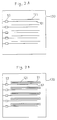
- Figures 2A-2D are schematic diagrams showing a production process of the substrate of Figure 1A.
- Figures 3A-3D are schematic diagrams showing a production process of the substrate of Figure 1B.
- Figure 4A is a plan view showing another active-matrix substrate used in this invention.
- Figures 4B and 4C are sectional views taken along lines B-B and C-C of Figure 4A.
- Figures 5A-5D are schematic diagrams showing a production process of the substrate of Figure 4B.
- Figures 6A-6D are schematic diagrams showing a production process of the substrate of Figure 4C.
- Figure 7 is a plan view showing still another active-matrix substrate used in this invention.
- FIGS 8A-8C are plan views showing other active-matrix substrates used in this invention.
- Figure 9A is a perspective view showing a conventional active-matrix display device.
- Figure 9B is a sectional view taken along line B-B of Figure 9A.
- Figure 9C is a schematic diagram showing the substrate of Figure 9A.
- Figure 10 is a plan view showing a region of the TFT in the substrate shown in Figure 9A.
- FIG. 11 is an equivalent circuit diagram of the TFT of Figure 10.
- Figure 12 is a plan view showing a conventional active-matrix substrate with added capacitance.
- Figures 13 and 14, respectively, are sectional views taken along lines P-P and Q-Q of Figure 12.
- Figure 15 is an equivalent circuit diagram of the substrate of Figure 12.
- Figure 1A is a plan view of the active-matrix substrate used in an active-matrix display device of this invention.
- Figure 1B is a cross sectional view of the substrate taken along line B-B of Figure 1A.
- Figures 2A through 2D and Figures 3A through 3D show a production process of the active-matrix substrate of Figure 1A.
- Figures 2A-2D are plan views showing the entire substrate of Figure 1A and Figures 3A-3D are sectional views taken along line B-B of Figure 1A.
- gate electrode wires 61 , gate electrode terminals 53 , secondary wires 121 , and a peripheral wire 130 are formed by a metal film on a glass substrate 50 .
- the gate electrode terminals 53 are positioned on the ends of the gate electrode wires 61 .
- the gate electrode terminals 53 are connected to the peripheral wire 130 .
- the peripheral wire 130 is positioned around the area where the gate electrode wires 61 and the secondary wires 121 are formed.
- an anodic oxide film 122 is formed on the gate electrode wires 61 by anodic oxidation ( Figure 3B).
- Anodic oxidation of the gate electrode wires 61 is performed by current flow via the peripheral wire 130 . Therefore, all of the gate electrode wires 61 undergo anodic oxidation at the same time.
- the added capacitance electrode wires 91 made of a transparent conductive film of ITO, SnO2, etc., are then formed so they cover the secondary wires 121 as shown in Figures 2B and 3C. Part of each of the added capacitance electrode wires 91 functions as an added capacitance electrode.
- the shape of the added capacitance electrode wire 91 in Figure 1A is shown in a rectangular shape in Figure 2B to simplify the diagram.
- the thickness of the added capacitance electrode wires 91 is 500-2000 ⁇ .
- a gate insulation film 101 of SiO2, SiNx, etc., is then laid over the entire surface of the substrate 50 (Figure 3D).
- the areas of gate insulation film 101 above the ends of the added capacitance electrode wires 91 are removed to make connection holes 131 ( Figure 2C).
- a connection wire 132 which electrically connects the added capacitance electrode wires 91 through each of the connection holes 131 , opposing electrode terminals 55 , source electrode wires 62 , and source electrode terminals 54 are formed at the same time.
- One end of the connection wire 132 is electrically connected to the opposing electrode terminal 55 , and when assembled as a display device, it is electrically connected to the opposing electrode.
- the source electrode terminals 54 are electrically connected to one end of each of the source electrode wires 62 .
- the picture element electrodes 64 are formed over the added capacitance electrode wires 91 in a manner so as to sandwich a gate insulation film 101 therebetween, and the peripheral wire 130 is separated from the gate electrode terminals 53 and the source electrode terminals 54 to yield the active-matrix substrate in Figure 1A.
- the added capacitance electrode wires 91 and gate insulation film 101 are formed on the stepped part of the secondary wires 121 , so there is a greater tendency that the covering of the added capacitance electrode wires 91 by the gate insulation film 101 becomes less complete than when there are no secondary wires 121 . Moreover, it is also possible for the insulation to become defective due to pin holes which form in the gate insulation film 101 , which causes more serious defects such as line defects.
- FIG 4A is a plan view of an example designed to solve the above-mentioned problem.
- TFTs 17 are formed as switching elements on the gate electrodes 19 connected to the gate electrode wires 5
- the source electrodes 14 of the TFTs 17 are connected to the source electrode wires 13
- the drain electrodes 15 thereof are connected to picture element electrodes 16 .
- the gate electrode wires 5 and the source electrode wires 13 intersect to sandwich a gate insulation film 8 therebetween, which will be described below.
- the added capacitance electrode wires 2 are positioned below the picture element electrodes 16 .
- Figure 4B and Figure 4C are cross sectional views taken along lines B-B and C-C of Figure 4A.
- Figures 5A to 5D show a production process for the substrate in Figure 4B.
- the added capacitance electrode wire 2 formed below the base insulation film 3 from a transparent conductive material is reduced during the production process and it loses its transparency, which is undesirable.
- the thickness of the base insulation film 3 is set at about 1000 ⁇ when a material with a small specific dielectric constant such as SiO2 (the specific dielectric constant thereof being 4 ) is used, but the thickness can be greater when a material with a large specific dielectric constant such as Ta2O5 (the specific dielectric constant thereof being 23-25) is used.
- the base insulation film 3 can have a multilayer structure in which a nitride film or an oxide film of a different material is formed on the above-mentioned oxide film. When a multilayer structure is used for the base insulation film 3 , the first layer that is in contact with the added capacitance electrode wire 2 below it must be formed using the oxide materials mentioned above for the same reason as mentioned above.
- the through-holes 4 were formed in the base insulation film 3 (Figure 5B).
- the through-holes 4 are provided to electrically connect the added capacitance electrode wires 2 and the secondary wires 6 to be formed later.
- the through-holes 4 were made in two places, but they may also be a continuous groove shape.
- Patterns are selectively formed in this Ta metal film by a dry etching technique when the base insulation film 3 is a SiO2 film and by a wet etching technique using a mixture of HF and HNO3 when the base insulation film 3 is a Ta2O5 film.
- the anodic oxide film 7 is formed by anodic oxidation of the surface of the secondary wires 6 , the gate electrode wires 5 ( Figure 5D) and the gate electrodes 19 .
- the Ta metal undergoes anodic oxidation in an ammonium borate solution, a citric acid solution or an ammonium tartrate solution, so a Ta2O5 is formed on the surface of the Ta metal.
- a gate insulation film 8 of SiNx was laid over the entire surface of this substrate to form the picture element electrodes 16 and yield the configuration shown in Figure 4B.
- FIGs 6A through 6D show a production process of the TFT 17 in Figure 4C.
- An anodic oxide film 7 was formed on the top of the gate electrodes 19 as described above, and then a SiNx gate insulation film 8 was formed over the entire surface of the base insulation film 3 including the anodic oxide film 7 .
- the entire surface of the substrate was then covered with an a-Si(i) layer 22 which serves as a semiconductor layer and a SiNx layer 10 which serves as an etching stop layer (Figure 6A).
- the SiNx layer 10 was then patterned in the prescribed shape, except for a part positioned above the gate electrodes 19 , so as to form the etching stop layer 11 ( Figure 6B).
- a-Si(n+) layer with a thickness of 1000 ⁇ (not shown) covering the etching stop layer 11 was formed by the plasma CVD method over the entire surface of the a-Si(i) layer 22 , the a-Si(n+) layer later becoming a contact layer.
- the a-Si(i) layer 22 and the a-Si(n+) layer were patterned in the prescribed shape to form the semiconductor layer 9 and the contact layer 12 ( Figure 6C).
- Ti, Mo or other metal was then laid over the entire surface of this substrate by spattering, and this metal film was patterned by an etching technique to form the source electrode wires 13 , the source electrodes 14 , and the drain electrodes 15 .
- a portion of the contact layer 12 on the etching stop layer 11 was also removed by etching so the contact layer 12 was divided into the part below the source electrode 14 and the part below the drain electrode 15 ( Figure 6D).
- ITO film with a thickness of 1000 ⁇ was then laid over the entire surface of the substrate by spattering. This ITO film was patterned in the prescribed shape to form the picture element electrodes 16 . The ITO film that is positioned above the source electrode wires 13 , the source electrodes 14 and the drain electrodes 15 was not removed in order to strengthen them (Figure 4C).
- an added capacitance is formed between each picture element electrodes 16 and part of the corresponding added capacitance electrode wire 2 .
- the secondary wires 6 are connected electrically to the added capacitance electrode wires 2 . Since an anodic oxide film 7 is formed on the top surface of the secondary wires 6 toward the picture element electrodes 16 , the occurrence of insulation defects between the secondary wires 6 and the picture element electrodes 16 can be reduced. Moreover, since there are two insulation films, the base insulation film 3 and the gate insulation film 8 , between the picture element electrodes 16 and the added capacitance electrode wires 2 , the occurrence of insulation defects between the added capacitance electrode wires 2 and the picture element electrodes 16 can also be reduced.
- Example 2 This example is intended to solve the problem arising in Example 1, in which the active-matrix substrate provided with added capacitance electrode wires 91 with secondary wires 121 , as explained in Figure 2C and Figure 2D, requires that the secondary wires 121 be connected to each other electrically, thus requiring an extra production process.
- FIG. 7 is a plan view showing the active-matrix substrate of this example in the course of the production.
- Gate electrode wires 43 that function as scanning lines, gate electrode terminals 44 , a secondary wire 6 , and a peripheral wire 41 are formed from a metal film on a glass substrate.
- Gate electrode wires 43 with gate electrode terminals at one end and gate electrode wires 43 with gate electrode terminals at the opposite ends were alternately disposed, and each of the gate electrode terminals 44 were connected to the peripheral wire 41 .
- the peripheral wire 41 was positioned around the area where the gate electrode wires 43 and the secondary wire 6 were formed.
- An anodic oxide film formed by means of an anodic oxidation current passing through the peripheral wire 41 was positioned over each of the gate electrode wires 43 .
- the secondary wire 6 was positioned in a zigzag manner between the gate electrode wires 43 .
- Opposing electrode terminals 45 for connecting to the opposing electrodes were formed on both ends of the secondary wire 6 .
- Added capacitance electrode wires 2 were formed from a transparent conductive material above those parts of the secondary wires 6 that were parallel to the gate electrode wires 43 .
- the shape of the added capacitance electrode wire 2 is shown rectangular in Figure 7.
- the configuration of the part where the added capacitance was formed in this example is the same as in the example shown in Figure 1B.
- a gate insulation film, picture element electrodes, TFTs, etc., were then formed to yield an active-matrix substrate.
- the wiring density was determined by the width of the gate electrode terminals since all of the gate electrode terminals were on one end of the gate electrode wires and the gate electrode terminals 44 were wider than the gate electrode wires 43 . In this example, however, high density wiring could be achieved because the gate electrode terminals 44 were alternately disposed.
- Figure 8A is a plan view of the active-matrix substrate of this example in the course of production.
- This example differs from that of Figure 7 in that the secondary wire 6 was connected to the peripheral wire 41 .
- the configuration of the part where the added capacitance was formed in this example was the same as the example shown in Figure 4B, and an anodic oxide film was formed on the top of the secondary wire 6 .
- anodic oxidation could be performed on the secondary wire 6 at the same time as the gate electrode wires 43 .
- Anodic oxidation was performed by forming a resist on the areas indicated by A1 and A2 using a printing technique or the like and then immersing the substrate in an anodic oxidation solution and applying a voltage thereto via the peripheral wire 41 .
- a single, continuous secondary wire 6 with no breaks was also formed in this example, so no process was required to electrically connect the secondary wires as in Example 1. Also, few connections with the peripheral wire 41 are required to perform anodic oxidation, so high-density wiring is possible. Moreover, high-density wiring can also be achieved by alternately disposing the gate electrode terminals 44 .
- a configuration is also possible in which the secondary wire 6 is connected to the opposing electrode terminals 45 in four places.
- a configuration is also possible in which the secondary wire is divided up into multiple wires, each of the secondary wires 6 has an opposing electrode terminal 45 , and the opposing electrode terminals 45 are connected to the peripheral wire 41 .
Landscapes
- Physics & Mathematics (AREA)
- Engineering & Computer Science (AREA)
- Nonlinear Science (AREA)
- Power Engineering (AREA)
- Microelectronics & Electronic Packaging (AREA)
- Mathematical Physics (AREA)
- Chemical & Material Sciences (AREA)
- Crystallography & Structural Chemistry (AREA)
- General Physics & Mathematics (AREA)
- Optics & Photonics (AREA)
- Liquid Crystal (AREA)
Claims (7)
- Aktivmatrix-Anzeigevorrichtung mit einem Paar isolierender Substrate, die einander gegenüberstehen; einer Anzahl von Abrasterleitungen (61, 5), die auf parallele Weise an der Innenseite eines der Substrate ausgebildet sind; einer Anzahl von Sourceleitungen (62, 13), die die Abrasterleitungen schneiden und auf parallele Weise an der Innenseite eines der Substrate (50, 1) angeordnet sind; einem optisch modulierbaren Anzeigemedium, das zwischen den isolierenden Substraten angeordnet ist; Bildelementelektroden (64, 16), die in einer Matrix auf der Innenseite eines der Substrate (50, 1) angeordnet sind; einer jeweiligen Schalteinrichtung auf dem einen Substrat für jede Bildelementelektrode und einer Anzahl von Elektrodenleitungen (91, 2) für eine Zusatzkapazität, von denen jede auf parallele Weise zwischen benachbarten Abrasterleitungen angeordnet ist, wobei die Elektrodenleitungen (91, 2) für die Zusatzkapazität aus einem transparenten, leitenden Film auf einem der Substrate (50, 1) bestehen und sie mindestens einen Isolierfilm (101, 8) zwischen der Bildelementelektrode und sich einbetten; gekennzeichnet durch eine Sekundärleitung (121, 6), die über oder unter jeder Elektrodenleitung für die Zusatzkapazität angeordnet ist und elektrisch mit dieser verbunden ist, so daß sich der effektive elektrische Widerstand der Elektrodenleitung für die Zusatzkapazität verringert.
- Aktivmatrix-Anzeigevorrichtung nach Anspruch 1, bei der die Sekundärleitung (6) so über der Elektrodenleitung (2) für die Zusatzkapazität angeordnet ist, daß sie einen Isolierfilm (3) dazwischen einbetten, der über einen Verbindungsgraben oder Durchgangslöcher (4) verfügt, durch die die Elektrodenleitung für die Zusatzkapazität und die Sekundärleitung elektrisch miteinander verbunden sind, und bei der ein anodischer Oxidationsfilm (7) auf der Sekundärleitung angeordnet ist.
- Aktivmatrix-Anzeigevorrichtung nach Anspruch 1, bei der ein jeweiliger Verbindungsanschluß an einem Ende jeder Abrasterleitung ausgebildet ist, wobei benachbarte Abrasterleitungen ihre Verbindungsanschlüsse an entgegengesetzten Enden aufweisen und wobei die Sekundärleitung aus ersten Teilen, die elektrisch mit entsprechenden der Elektrodenleitungen für die Zusatzkapazität verbunden sind, um parallel zu den Abrasterleitungen zu liegen, und zweiten Teilen besteht, die elektrisch mit den ersten Teilen an den anschlußfreien Enden der dazwischenliegenden Abrasterleitungen mit der Sekundärleitung verbunden sind, so daß die Sekundärleitung auf Zickzackweise angeordnet ist.
- Aktivmatrix-Anzeigevorrichtung nach Anspruch 3, bei der die Sekundärleitung so ausgebildet ist, daß sie in mehrere Teilbereiche unterteilt ist.
- Verfahren zum Herstellen der Aktivmatrix-Anzeigevorrichtung gemäß Anspruch 1, in der die Schalteinrichtung einen Dünnfilmtransistor aufweist, gekennzeichnet durch:
- Mustern einer leitenden Schicht auf der Innenseite des einen Substrats (50), um gleichzeitig Gateelektroden der Dünnfilmtransistoren, Gateelektrodenleitungen (61) als Abrasterleitungen und die Sekundärleitung (121) auszubilden. - Verfahren nach Anspruch 5, mit den folgenden Schritten:- Ausbilden der Elektrodenleitung für die Zusatzkapazität auf der Innenseite des einen Substrats;- Ausbilden eines ersten Isolierfilms auf der Elektrodenleitung für die Zusatzkapazität;- Ausbilden eines Verbindungsgrabens oder von Durchgangslöchern im Isolierfilm;- Ausbilden der leitenden Schicht auf der gesamten Oberfläche des ersten Isolierfilms einschließlich des Verbindungsgrabens oder der Durchgangslöcher;- Ausführen der genannten Musterbildung der leitenden Schicht;- Ausbilden eines zweiten Isolierfilms auf der gesamten Oberfläche des ersten Isolierfilms, auf dem die Sekundärleitung ausgebildet wurde; und- Ausbilden der Bildelementelektroden auf dem zweiten Isolierfilm.
- Verfahren nach Anspruch 5, mit den folgenden Schritten:- Ausbilden der leitenden Schicht auf der Innenseite des einen Substrats;- Ausführen der genannten Musterbildung auf der leitenden Schicht;- Ausbilden der Elektrodenleitung für die Zusatzkapazität, um die Sekundärleitung mit ihr abzudecken;- Ausbilden des Isolierfilms auf der Elektrodenleitung für die Zusatzkapazität und- Ausbilden der Bildelementelektroden auf dem Isolierfilm.
Applications Claiming Priority (4)
| Application Number | Priority Date | Filing Date | Title |
|---|---|---|---|
| JP13337289A JPH07113728B2 (ja) | 1989-05-26 | 1989-05-26 | アクティブマトリクス基板 |
| JP133372/89 | 1989-05-26 | ||
| JP170808/89 | 1989-06-30 | ||
| JP17080889A JPH0820641B2 (ja) | 1989-06-30 | 1989-06-30 | 液晶表示装置の製造方法 |
Publications (3)
| Publication Number | Publication Date |
|---|---|
| EP0399846A2 EP0399846A2 (de) | 1990-11-28 |
| EP0399846A3 EP0399846A3 (de) | 1991-07-24 |
| EP0399846B1 true EP0399846B1 (de) | 1995-03-01 |
Family
ID=26467747
Family Applications (1)
| Application Number | Title | Priority Date | Filing Date |
|---|---|---|---|
| EP90305754A Expired - Lifetime EP0399846B1 (de) | 1989-05-26 | 1990-05-25 | Aktiv-Matrix-Anzeigevorrichtung und Verfahren zu ihrer Herstellung |
Country Status (3)
| Country | Link |
|---|---|
| US (1) | US5162901A (de) |
| EP (1) | EP0399846B1 (de) |
| DE (1) | DE69017262T2 (de) |
Cited By (3)
| Publication number | Priority date | Publication date | Assignee | Title |
|---|---|---|---|---|
| US6566711B1 (en) | 1991-08-23 | 2003-05-20 | Semiconductor Energy Laboratory Co., Ltd. | Semiconductor device having interlayer insulating film |
| US8324027B2 (en) | 2009-07-10 | 2012-12-04 | Semiconductor Energy Laboratory Co., Ltd. | Semiconductor device and method for manufacturing the same |
| US8384085B2 (en) | 2009-08-07 | 2013-02-26 | Semiconductor Energy Laboratory Co., Ltd. | Semiconductor device and method for manufacturing the same |
Families Citing this family (47)
| Publication number | Priority date | Publication date | Assignee | Title |
|---|---|---|---|---|
| FR2662290B1 (fr) * | 1990-05-15 | 1992-07-24 | France Telecom | Procede de realisation d'un ecran d'affichage a matrice active et a condensateurs de stockage et ecran obtenu par ce procede. |
| JP2650780B2 (ja) * | 1990-11-30 | 1997-09-03 | シャープ株式会社 | アクティブマトリクス基板 |
| JP2999271B2 (ja) * | 1990-12-10 | 2000-01-17 | 株式会社半導体エネルギー研究所 | 表示装置 |
| EP0499979A3 (en) | 1991-02-16 | 1993-06-09 | Semiconductor Energy Laboratory Co., Ltd. | Electro-optical device |
| US5854494A (en) * | 1991-02-16 | 1998-12-29 | Semiconductor Energy Laboratory Co., Ltd. | Electric device, matrix device, electro-optical display device, and semiconductor memory having thin-film transistors |
| US6028333A (en) * | 1991-02-16 | 2000-02-22 | Semiconductor Energy Laboratory Co., Ltd. | Electric device, matrix device, electro-optical display device, and semiconductor memory having thin-film transistors |
| US5521107A (en) * | 1991-02-16 | 1996-05-28 | Semiconductor Energy Laboratory Co., Ltd. | Method for forming a field-effect transistor including anodic oxidation of the gate |
| JP3556679B2 (ja) | 1992-05-29 | 2004-08-18 | 株式会社半導体エネルギー研究所 | 電気光学装置 |
| US6979840B1 (en) * | 1991-09-25 | 2005-12-27 | Semiconductor Energy Laboratory Co., Ltd. | Thin film transistors having anodized metal film between the gate wiring and drain wiring |
| JP2900662B2 (ja) * | 1991-10-18 | 1999-06-02 | 三菱電機株式会社 | 薄膜トランジスタアレイ |
| US5422293A (en) * | 1991-12-24 | 1995-06-06 | Casio Computer Co., Ltd. | Method for manufacturing a TFT panel |
| DE69319760T2 (de) * | 1992-02-21 | 1999-02-11 | International Business Machines Corp., Armonk, N.Y. | Flüssigkristallanzeigevorrichtung |
| US5402141A (en) * | 1992-03-11 | 1995-03-28 | Honeywell Inc. | Multigap liquid crystal color display with reduced image retention and flicker |
| JP3133140B2 (ja) * | 1992-04-01 | 2001-02-05 | 株式会社半導体エネルギー研究所 | 表示装置 |
| JP2814161B2 (ja) | 1992-04-28 | 1998-10-22 | 株式会社半導体エネルギー研究所 | アクティブマトリクス表示装置およびその駆動方法 |
| JP3245959B2 (ja) * | 1992-06-05 | 2002-01-15 | 松下電器産業株式会社 | 液晶画像表示装置の製造方法 |
| EP0592063A3 (en) * | 1992-09-14 | 1994-07-13 | Toshiba Kk | Active matrix liquid crystal display device |
| US6313889B1 (en) * | 1993-03-04 | 2001-11-06 | Samsung Electronics Co., Ltd. | Matrix-type display device capable of being repaired in pixel unit |
| JP3258768B2 (ja) * | 1993-06-22 | 2002-02-18 | 三菱電機株式会社 | マトリックス型表示装置 |
| US5852480A (en) * | 1994-03-30 | 1998-12-22 | Nec Corporation | LCD panel having a plurality of shunt buses |
| JP3402400B2 (ja) | 1994-04-22 | 2003-05-06 | 株式会社半導体エネルギー研究所 | 半導体集積回路の作製方法 |
| US6747627B1 (en) | 1994-04-22 | 2004-06-08 | Semiconductor Energy Laboratory Co., Ltd. | Redundancy shift register circuit for driver circuit in active matrix type liquid crystal display device |
| JP2827920B2 (ja) * | 1994-10-13 | 1998-11-25 | 松下電器産業株式会社 | カラー液晶表示パネル |
| KR100338480B1 (ko) * | 1995-08-19 | 2003-01-24 | 엘지.필립스 엘시디 주식회사 | 액정표시장치및그제조방법 |
| JP3737176B2 (ja) | 1995-12-21 | 2006-01-18 | 株式会社半導体エネルギー研究所 | 液晶表示装置 |
| JP3624596B2 (ja) * | 1996-12-09 | 2005-03-02 | ソニー株式会社 | 画像表示装置 |
| US5892558A (en) * | 1997-06-26 | 1999-04-06 | Gl Displays, Inc. | Wire electrode structure based on 2 or 3 terminal device employed in a liquid crystal display |
| US6600157B2 (en) * | 2000-06-27 | 2003-07-29 | Canon Kabushiki Kaisha | Semiconductor device, and radiation detection device and radiation detection system having same |
| GB0029315D0 (en) * | 2000-12-01 | 2001-01-17 | Koninkl Philips Electronics Nv | Method of increasing the conductivity of a transparent conductive layer |
| JP3909572B2 (ja) * | 2001-09-28 | 2007-04-25 | 株式会社日立製作所 | 表示装置 |
| TW594156B (en) * | 2002-01-04 | 2004-06-21 | Fujitsu Display Tech | Substrate for display device and display device equipped therewith |
| US8247965B2 (en) * | 2003-11-14 | 2012-08-21 | Semiconductor Energy Laboratory Co., Ltd. | Light emitting display device and method for manufacturing the same |
| US7439086B2 (en) * | 2003-11-14 | 2008-10-21 | Semiconductor Energy Laboratory Co., Ltd. | Method for manufacturing liquid crystal display device |
| US8089434B2 (en) * | 2005-12-12 | 2012-01-03 | Nupix, LLC | Electroded polymer substrate with embedded wires for an electronic display |
| JP2009519564A (ja) * | 2005-12-12 | 2009-05-14 | モア ビー. チャド | ワイヤ式のフラットパネルディスプレイ |
| US8166649B2 (en) * | 2005-12-12 | 2012-05-01 | Nupix, LLC | Method of forming an electroded sheet |
| US8106853B2 (en) * | 2005-12-12 | 2012-01-31 | Nupix, LLC | Wire-based flat panel displays |
| US20070132387A1 (en) * | 2005-12-12 | 2007-06-14 | Moore Chad B | Tubular plasma display |
| US8441007B2 (en) | 2008-12-25 | 2013-05-14 | Semiconductor Energy Laboratory Co., Ltd. | Display device and manufacturing method thereof |
| US20100224878A1 (en) | 2009-03-05 | 2010-09-09 | Semiconductor Energy Laboratory Co., Ltd. | Semiconductor device |
| US8461582B2 (en) | 2009-03-05 | 2013-06-11 | Semiconductor Energy Laboratory Co., Ltd. | Semiconductor device and method for manufacturing the same |
| KR101746198B1 (ko) | 2009-09-04 | 2017-06-12 | 가부시키가이샤 한도오따이 에네루기 켄큐쇼 | 표시장치 및 전자기기 |
| WO2011049230A1 (en) | 2009-10-21 | 2011-04-28 | Semiconductor Energy Laboratory Co., Ltd. | Voltage regulator circuit |
| EP2513893A4 (de) | 2009-12-18 | 2016-09-07 | Semiconductor Energy Lab | Flüssigkristallanzeigevorrichtung und elektronische vorrichtung |
| KR101873730B1 (ko) * | 2010-01-24 | 2018-07-04 | 가부시키가이샤 한도오따이 에네루기 켄큐쇼 | 표시 장치 |
| KR101132119B1 (ko) * | 2010-03-10 | 2012-04-05 | 삼성모바일디스플레이주식회사 | 액정표시장치 어레이 기판 및 그 제조방법 |
| US8569754B2 (en) | 2010-11-05 | 2013-10-29 | Semiconductor Energy Laboratory Co., Ltd. | Semiconductor device and manufacturing method thereof |
Family Cites Families (24)
| Publication number | Priority date | Publication date | Assignee | Title |
|---|---|---|---|---|
| GB2081018B (en) * | 1980-07-31 | 1985-06-26 | Suwa Seikosha Kk | Active matrix assembly for display device |
| JPS57115856A (en) * | 1981-01-09 | 1982-07-19 | Semiconductor Energy Lab Co Ltd | Compound semiconductor device |
| JPS5821863A (ja) * | 1981-07-31 | 1983-02-08 | Seiko Epson Corp | 液晶表示装置 |
| JPS58130561A (ja) * | 1982-01-29 | 1983-08-04 | Seiko Epson Corp | アクテイブマトリクス基板 |
| JPS58159518A (ja) * | 1982-03-18 | 1983-09-21 | Seiko Epson Corp | 液晶表示パネル |
| JPS595229A (ja) * | 1982-07-01 | 1984-01-12 | Asahi Glass Co Ltd | 画像表示装置 |
| JPH06100745B2 (ja) * | 1982-07-02 | 1994-12-12 | セイコーエプソン株式会社 | アクティブマトリクス型液晶表示装置 |
| JPS5961818A (ja) * | 1982-10-01 | 1984-04-09 | Seiko Epson Corp | 液晶表示装置 |
| JPS60169828A (ja) * | 1984-02-15 | 1985-09-03 | Hitachi Ltd | 液晶表示素子の電極基板 |
| JPS60239711A (ja) * | 1984-05-14 | 1985-11-28 | Canon Inc | トランジスタの駆動法 |
| JPS60230118A (ja) * | 1984-04-27 | 1985-11-15 | Seiko Instr & Electronics Ltd | 記憶容量内蔵型液晶表示装置 |
| JPH0646277B2 (ja) * | 1984-04-27 | 1994-06-15 | セイコー電子工業株式会社 | 記憶容量内蔵型液晶表示装置 |
| JPS6129820A (ja) * | 1984-07-23 | 1986-02-10 | Seiko Instr & Electronics Ltd | アクテイプマトリクス表示装置用基板 |
| JPS61151516A (ja) * | 1984-12-25 | 1986-07-10 | Seiko Instr & Electronics Ltd | Mis型アクテイプマトリクス表示装置用基板 |
| JPS61243430A (ja) * | 1985-04-22 | 1986-10-29 | Canon Inc | 液晶装置 |
| JPH0685032B2 (ja) * | 1985-10-17 | 1994-10-26 | キヤノン株式会社 | カイラルスメクティック液晶素子 |
| JPS6290624A (ja) * | 1985-10-17 | 1987-04-25 | Asahi Glass Co Ltd | 画像表示装置 |
| JPS62227130A (ja) * | 1986-03-28 | 1987-10-06 | Nec Corp | アクテイブマトリクス型液晶表示装置 |
| JPS62296123A (ja) * | 1986-06-17 | 1987-12-23 | Toshiba Corp | アクテイブマトリツクス型液晶表示装置 |
| JPS62148929A (ja) * | 1986-10-27 | 1987-07-02 | Seiko Epson Corp | 液晶表示装置 |
| EP0288011A3 (de) * | 1987-04-20 | 1991-02-20 | Hitachi, Ltd. | Flüssigkristallanzeigeeinrichtung und Steuerungsverfahren dafür |
| JP2566149B2 (ja) * | 1987-09-10 | 1996-12-25 | キヤノン株式会社 | 光学変調素子 |
| JP2568857B2 (ja) * | 1987-09-22 | 1997-01-08 | セイコーエプソン株式会社 | アクティブマトリックス基板 |
| JPH0827465B2 (ja) * | 1988-04-06 | 1996-03-21 | 株式会社日立製作所 | 平面デイスプレイ |
-
1990
- 1990-05-23 US US07/527,191 patent/US5162901A/en not_active Expired - Lifetime
- 1990-05-25 DE DE69017262T patent/DE69017262T2/de not_active Expired - Fee Related
- 1990-05-25 EP EP90305754A patent/EP0399846B1/de not_active Expired - Lifetime
Cited By (6)
| Publication number | Priority date | Publication date | Assignee | Title |
|---|---|---|---|---|
| US6566711B1 (en) | 1991-08-23 | 2003-05-20 | Semiconductor Energy Laboratory Co., Ltd. | Semiconductor device having interlayer insulating film |
| US6977392B2 (en) | 1991-08-23 | 2005-12-20 | Semiconductor Energy Laboratory Co., Ltd. | Semiconductor display device |
| US8324027B2 (en) | 2009-07-10 | 2012-12-04 | Semiconductor Energy Laboratory Co., Ltd. | Semiconductor device and method for manufacturing the same |
| US8441011B2 (en) | 2009-07-10 | 2013-05-14 | Semiconductor Energy Laboratory Co., Ltd. | Semiconductor device and method for manufacturing the same |
| US8835920B2 (en) | 2009-07-10 | 2014-09-16 | Semiconductor Energy Laboratory Co., Ltd. | Semiconductor device and method for manufacturing the same |
| US8384085B2 (en) | 2009-08-07 | 2013-02-26 | Semiconductor Energy Laboratory Co., Ltd. | Semiconductor device and method for manufacturing the same |
Also Published As
| Publication number | Publication date |
|---|---|
| EP0399846A2 (de) | 1990-11-28 |
| EP0399846A3 (de) | 1991-07-24 |
| DE69017262D1 (de) | 1995-04-06 |
| US5162901A (en) | 1992-11-10 |
| DE69017262T2 (de) | 1995-09-21 |
Similar Documents
| Publication | Publication Date | Title |
|---|---|---|
| EP0399846B1 (de) | Aktiv-Matrix-Anzeigevorrichtung und Verfahren zu ihrer Herstellung | |
| KR100271037B1 (ko) | 액정 표시 장치의 구조 및 그 액정 표시 장치의 제조 방법(liquid crystal display device and the method for manufacturing the same) | |
| US5825449A (en) | Liquid crystal display device and method of manufacturing the same | |
| US5835177A (en) | Array substrate with bus lines takeout/terminal sections having multiple conductive layers | |
| USRE39798E1 (en) | Active matrix LCD device with image signal lines having a multilayered structure | |
| KR100374435B1 (ko) | 액정 표시 장치 및 그 제조 방법 | |
| US6411348B2 (en) | Active matrix substrate and producing method of the same | |
| KR100271067B1 (ko) | 액정표시장치 및 그 제조 방법 | |
| US20020171108A1 (en) | Thin film transistor array substrate for liquid cystal display and a method for fabricating the same | |
| US5796448A (en) | Structure for a parasitic capacitor and a storage capacitor in a thin film transistor-liquid crystal display and a method for making the same | |
| EP0329887B1 (de) | Flüssigkristall-Anzeigevorrichtung | |
| JPH0814669B2 (ja) | マトリクス型表示装置 | |
| US6654074B1 (en) | Array substrate for liquid crystal display device with shorting bars external to a data pad and method of manufacturing the same | |
| JP2682997B2 (ja) | 補助容量付液晶表示装置及び補助容量付液晶表示装置の製造方法 | |
| US5714769A (en) | Device of thin film transistor liquid crystal display | |
| US5686976A (en) | Liquid crystal display with storage capacitors for holding electric charges | |
| EP0605176B1 (de) | Flüssigkristall-Anzeigetafel mit aktiver Matrix und Verfahren zu ihrer Herstellung | |
| US5657101A (en) | LCD having a thin film capacitor with two lower capacitor electrodes and a pixel electrode serving as an upper electrode | |
| JPH07113728B2 (ja) | アクティブマトリクス基板 | |
| EP0488802B1 (de) | Anzeigevorrichtung mit aktiver Matrix | |
| JP2800958B2 (ja) | アクティブマトリクス基板 | |
| US5861635A (en) | Liquid crystal display including a coplanar line structure | |
| US5994155A (en) | Method of fabricating a thin film transistor liquid crystal display | |
| EP0567684A1 (de) | Elektrooptische Vorrichtung | |
| JPH0862629A (ja) | 液晶表示装置 |
Legal Events
| Date | Code | Title | Description |
|---|---|---|---|
| PUAI | Public reference made under article 153(3) epc to a published international application that has entered the european phase |
Free format text: ORIGINAL CODE: 0009012 |
|
| AK | Designated contracting states |
Kind code of ref document: A2 Designated state(s): DE FR GB |
|
| 17P | Request for examination filed |
Effective date: 19901228 |
|
| PUAL | Search report despatched |
Free format text: ORIGINAL CODE: 0009013 |
|
| AK | Designated contracting states |
Kind code of ref document: A3 Designated state(s): DE FR GB |
|
| 17Q | First examination report despatched |
Effective date: 19930709 |
|
| GRAA | (expected) grant |
Free format text: ORIGINAL CODE: 0009210 |
|
| AK | Designated contracting states |
Kind code of ref document: B1 Designated state(s): DE FR GB |
|
| REF | Corresponds to: |
Ref document number: 69017262 Country of ref document: DE Date of ref document: 19950406 |
|
| ET | Fr: translation filed | ||
| PLBE | No opposition filed within time limit |
Free format text: ORIGINAL CODE: 0009261 |
|
| STAA | Information on the status of an ep patent application or granted ep patent |
Free format text: STATUS: NO OPPOSITION FILED WITHIN TIME LIMIT |
|
| 26N | No opposition filed | ||
| PGFP | Annual fee paid to national office [announced via postgrant information from national office to epo] |
Ref country code: FR Payment date: 20010518 Year of fee payment: 12 |
|
| PGFP | Annual fee paid to national office [announced via postgrant information from national office to epo] |
Ref country code: DE Payment date: 20010522 Year of fee payment: 12 |
|
| PGFP | Annual fee paid to national office [announced via postgrant information from national office to epo] |
Ref country code: GB Payment date: 20010523 Year of fee payment: 12 |
|
| REG | Reference to a national code |
Ref country code: GB Ref legal event code: IF02 |
|
| PG25 | Lapsed in a contracting state [announced via postgrant information from national office to epo] |
Ref country code: GB Free format text: LAPSE BECAUSE OF NON-PAYMENT OF DUE FEES Effective date: 20020525 |
|
| PG25 | Lapsed in a contracting state [announced via postgrant information from national office to epo] |
Ref country code: DE Free format text: LAPSE BECAUSE OF NON-PAYMENT OF DUE FEES Effective date: 20021203 |
|
| GBPC | Gb: european patent ceased through non-payment of renewal fee |
Effective date: 20020525 |
|
| PG25 | Lapsed in a contracting state [announced via postgrant information from national office to epo] |
Ref country code: FR Free format text: LAPSE BECAUSE OF NON-PAYMENT OF DUE FEES Effective date: 20030131 |
|
| REG | Reference to a national code |
Ref country code: FR Ref legal event code: ST |