EP0405183A2 - Isolation diélectrique pour procédé IC de haute puissance à haute tension - Google Patents
Isolation diélectrique pour procédé IC de haute puissance à haute tension Download PDFInfo
- Publication number
- EP0405183A2 EP0405183A2 EP90110524A EP90110524A EP0405183A2 EP 0405183 A2 EP0405183 A2 EP 0405183A2 EP 90110524 A EP90110524 A EP 90110524A EP 90110524 A EP90110524 A EP 90110524A EP 0405183 A2 EP0405183 A2 EP 0405183A2
- Authority
- EP
- European Patent Office
- Prior art keywords
- wafer
- transistor
- forming
- oxide
- high voltage
- Prior art date
- Legal status (The legal status is an assumption and is not a legal conclusion. Google has not performed a legal analysis and makes no representation as to the accuracy of the status listed.)
- Ceased
Links
Images

Classifications
-
- H—ELECTRICITY
- H10—SEMICONDUCTOR DEVICES; ELECTRIC SOLID-STATE DEVICES NOT OTHERWISE PROVIDED FOR
- H10P—GENERIC PROCESSES OR APPARATUS FOR THE MANUFACTURE OR TREATMENT OF DEVICES COVERED BY CLASS H10
- H10P90/00—Preparation of wafers not covered by a single main group of this subclass, e.g. wafer reinforcement
- H10P90/19—Preparing inhomogeneous wafers
- H10P90/1904—Preparing vertically inhomogeneous wafers
- H10P90/1906—Preparing SOI wafers
- H10P90/1914—Preparing SOI wafers using bonding
-
- H—ELECTRICITY
- H10—SEMICONDUCTOR DEVICES; ELECTRIC SOLID-STATE DEVICES NOT OTHERWISE PROVIDED FOR
- H10D—INORGANIC ELECTRIC SEMICONDUCTOR DEVICES
- H10D84/00—Integrated devices formed in or on semiconductor substrates that comprise only semiconducting layers, e.g. on Si wafers or on GaAs-on-Si wafers
- H10D84/80—Integrated devices formed in or on semiconductor substrates that comprise only semiconducting layers, e.g. on Si wafers or on GaAs-on-Si wafers characterised by the integration of at least one component covered by groups H10D12/00 or H10D30/00, e.g. integration of IGFETs
- H10D84/82—Integrated devices formed in or on semiconductor substrates that comprise only semiconducting layers, e.g. on Si wafers or on GaAs-on-Si wafers characterised by the integration of at least one component covered by groups H10D12/00 or H10D30/00, e.g. integration of IGFETs of only field-effect components
- H10D84/83—Integrated devices formed in or on semiconductor substrates that comprise only semiconducting layers, e.g. on Si wafers or on GaAs-on-Si wafers characterised by the integration of at least one component covered by groups H10D12/00 or H10D30/00, e.g. integration of IGFETs of only field-effect components of only insulated-gate FETs [IGFET]
- H10D84/837—Integrated devices formed in or on semiconductor substrates that comprise only semiconducting layers, e.g. on Si wafers or on GaAs-on-Si wafers characterised by the integration of at least one component covered by groups H10D12/00 or H10D30/00, e.g. integration of IGFETs of only field-effect components of only insulated-gate FETs [IGFET] comprising vertical IGFETs
- H10D84/839—Integrated devices formed in or on semiconductor substrates that comprise only semiconducting layers, e.g. on Si wafers or on GaAs-on-Si wafers characterised by the integration of at least one component covered by groups H10D12/00 or H10D30/00, e.g. integration of IGFETs of only field-effect components of only insulated-gate FETs [IGFET] comprising vertical IGFETs comprising VDMOS
-
- H—ELECTRICITY
- H10—SEMICONDUCTOR DEVICES; ELECTRIC SOLID-STATE DEVICES NOT OTHERWISE PROVIDED FOR
- H10W—GENERIC PACKAGES, INTERCONNECTIONS, CONNECTORS OR OTHER CONSTRUCTIONAL DETAILS OF DEVICES COVERED BY CLASS H10
- H10W10/00—Isolation regions in semiconductor bodies between components of integrated devices
- H10W10/10—Isolation regions comprising dielectric materials
- H10W10/181—Semiconductor-on-insulator [SOI] isolation regions, e.g. buried oxide regions of SOI wafers
-
- H—ELECTRICITY
- H10—SEMICONDUCTOR DEVICES; ELECTRIC SOLID-STATE DEVICES NOT OTHERWISE PROVIDED FOR
- H10D—INORGANIC ELECTRIC SEMICONDUCTOR DEVICES
- H10D84/00—Integrated devices formed in or on semiconductor substrates that comprise only semiconducting layers, e.g. on Si wafers or on GaAs-on-Si wafers
- H10D84/40—Integrated devices formed in or on semiconductor substrates that comprise only semiconducting layers, e.g. on Si wafers or on GaAs-on-Si wafers characterised by the integration of at least one component covered by groups H10D12/00 or H10D30/00 with at least one component covered by groups H10D10/00 or H10D18/00, e.g. integration of IGFETs with BJTs
- H10D84/401—Combinations of FETs or IGBTs with BJTs
-
- H—ELECTRICITY
- H10—SEMICONDUCTOR DEVICES; ELECTRIC SOLID-STATE DEVICES NOT OTHERWISE PROVIDED FOR
- H10D—INORGANIC ELECTRIC SEMICONDUCTOR DEVICES
- H10D84/00—Integrated devices formed in or on semiconductor substrates that comprise only semiconducting layers, e.g. on Si wafers or on GaAs-on-Si wafers
- H10D84/80—Integrated devices formed in or on semiconductor substrates that comprise only semiconducting layers, e.g. on Si wafers or on GaAs-on-Si wafers characterised by the integration of at least one component covered by groups H10D12/00 or H10D30/00, e.g. integration of IGFETs
- H10D84/82—Integrated devices formed in or on semiconductor substrates that comprise only semiconducting layers, e.g. on Si wafers or on GaAs-on-Si wafers characterised by the integration of at least one component covered by groups H10D12/00 or H10D30/00, e.g. integration of IGFETs of only field-effect components
- H10D84/83—Integrated devices formed in or on semiconductor substrates that comprise only semiconducting layers, e.g. on Si wafers or on GaAs-on-Si wafers characterised by the integration of at least one component covered by groups H10D12/00 or H10D30/00, e.g. integration of IGFETs of only field-effect components of only insulated-gate FETs [IGFET]
-
- Y—GENERAL TAGGING OF NEW TECHNOLOGICAL DEVELOPMENTS; GENERAL TAGGING OF CROSS-SECTIONAL TECHNOLOGIES SPANNING OVER SEVERAL SECTIONS OF THE IPC; TECHNICAL SUBJECTS COVERED BY FORMER USPC CROSS-REFERENCE ART COLLECTIONS [XRACs] AND DIGESTS
- Y10—TECHNICAL SUBJECTS COVERED BY FORMER USPC
- Y10S—TECHNICAL SUBJECTS COVERED BY FORMER USPC CROSS-REFERENCE ART COLLECTIONS [XRACs] AND DIGESTS
- Y10S148/00—Metal treatment
- Y10S148/012—Bonding, e.g. electrostatic for strain gauges
-
- Y—GENERAL TAGGING OF NEW TECHNOLOGICAL DEVELOPMENTS; GENERAL TAGGING OF CROSS-SECTIONAL TECHNOLOGIES SPANNING OVER SEVERAL SECTIONS OF THE IPC; TECHNICAL SUBJECTS COVERED BY FORMER USPC CROSS-REFERENCE ART COLLECTIONS [XRACs] AND DIGESTS
- Y10—TECHNICAL SUBJECTS COVERED BY FORMER USPC
- Y10S—TECHNICAL SUBJECTS COVERED BY FORMER USPC CROSS-REFERENCE ART COLLECTIONS [XRACs] AND DIGESTS
- Y10S148/00—Metal treatment
- Y10S148/026—Deposition thru hole in mask
-
- Y—GENERAL TAGGING OF NEW TECHNOLOGICAL DEVELOPMENTS; GENERAL TAGGING OF CROSS-SECTIONAL TECHNOLOGIES SPANNING OVER SEVERAL SECTIONS OF THE IPC; TECHNICAL SUBJECTS COVERED BY FORMER USPC CROSS-REFERENCE ART COLLECTIONS [XRACs] AND DIGESTS
- Y10—TECHNICAL SUBJECTS COVERED BY FORMER USPC
- Y10S—TECHNICAL SUBJECTS COVERED BY FORMER USPC CROSS-REFERENCE ART COLLECTIONS [XRACs] AND DIGESTS
- Y10S148/00—Metal treatment
- Y10S148/135—Removal of substrate
Definitions
- Dielectric isolation is employed to fabricate semiconductor devices wherein metal-oxide-semiconductor (MOS) or other integrated circuit (IC) elements can be combined with a bipolar junction transistor (BJT), double diffused metal-oxide semiconductor (DMOS) or other high voltage semiconductor device.
- MOS metal-oxide-semiconductor
- BJT bipolar junction transistor
- DMOS double diffused metal-oxide semiconductor
- the DMOS transistor is capable of controlling large currents and is widely regarded as a favored way to control large amounts of power.
- the oxidized wafers can be washed to develop hydrophilic surfaces, a strong bond forms at room temperature when the wafer faces are placed together.
- a subsequent heat treatment causes the oxides to join together to form a buried oxide which can act to electrically isolate the material in the two wafers.
- the first wafer can then be ground and etched to provide the desired thickness of N type material which exists over an N + layer that faces the dielectric isolation.
- the resulting composite semiconductor wafer can be trench etched to isolate a plurality of N type tubs and the trench faces oxidized to complete the dielectric isolation. If desired, the oxidized trenches can be back filled with polycrystalline silicon (polysilicon).
- a deep trench can be etched through the N type wafer, its N + region and the dielectric whereby the second, or N+, wafer is exposed. Then an epitaxial deposition is employed to fill the deep trench with semiconductor material having a resistivity suitable for the DMOS transistor drain and the wafer ground and polished to restore the surface.
- the gate oxide and gate conductor typically doped polysilicon
- a double diffusion produces the source and channel regions in the surface of the exposed semiconductor.
- a metal electrode located over the diffusions so as to short them together in a second region, provides the DMOS source electrode.
- the drain electrode is available at the N + substrate formed by the second wafer. Electrically it is the backside of the composite wafer structure.
- the region of the composite wafer structure, where the epitaxially backfilled trench is located, will contain a power switch while the adjacent region will contain MOS or BJT devices. These latter devices are conventional and they are isolated by means of diffusions or groove etching of the N and N + layers in the first wafer.
- the power switch region can contain a DMOS device which has its drain dedicated to the composite wafer backside.
- the resulting breakdown voltage is not as high as might be desired.
- the Toshiba Corporation Intelligent Power Switches are rated at 60 and 100 volts for two and twenty ampere devices.
- a first N+ silicon wafer is provided with an N type epitaxial layer having a resistivity and thickness suitable for the DMOS transistor drain.
- the wafer surface is polished to a mirror finish and oxidized.
- a second wafer having a resistivity suitable for low voltage IC manufacturing has its face polished to a mirror finish and oxidized.
- the oxidized faces are then washed and pressed together with the resultant hydrophilic surface bonding.
- the assembled wafers are then heat treated to cause the oxides to merge, thus forming a composite wafer having an oxide isolation buried layer.
- the thickness of the second layer is reduced by a combination of grinding or lapping and etching to a predetermined thickness.
- the composite wafer is trench etched where high voltage transistors are to be created.
- This trench is made to penetrate the oxide isolation and to extend into the epitaxial layer material of the first wafer.
- epitaxial silicon is deposited to backfill the trench so that it extends the first wafer to fill the trench.
- Lapping and etching are then employed to render the surface flat and to leave the trench filled with epitaxial material.
- the material that now exists over the oxide isolation is on the order of about three microns thick. This layer can easily be penetrated by diffusion or trench ethcing to isolate tubs for low voltage IC fabrication.
- the thin epitaxial layer exists over the original epitaxial layer provided over the first wafer substrate.
- the material can easily be made thick enough to provide breakdown voltages in excess of 1000 volts.
- a vertical NPN transistor, vertical DMOS or other vertical power device is fabricated therein it can be made to have a very high breakdown voltage.
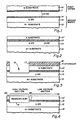
- a first silicon wafer 10 of N type conductivity is provided with an oxide film 11.
- the resistivity which is typically 1-10 ohm centimeters, is chosen to provide the proper value for fabricating the low voltage circuit elements.
- the wafer, of which a fragment is shown is typically about 500-700 microns thick and is first polished to produce an extremely flat mirror finish. The face is then oxidized to form oxide 11 to a thickness of about a micron.
- a second silicon wafer 12 having a resistivity of .0005 to .02 ohm centimeters and a thickness of about 500-700 microns is provided with one or more epitaxial layers represented by 13. This layer is typically about 20-100 microns thick and has a resistivity of about 10-100 ohm centimeters.
- the surface of epitaxial layer 13 is polished to a mirror finish and provided with an oxide layer 14.
- the two wafers are washed to render the oxide surfaces hydrophilic and they are pressed together.
- the extremely smooth hydrophilic oxides will cling together and form a strong bond between the two wafers.
- a subsequent heat treatment will cause the oxides to coalesce together to form a unitary oxide 15 of figure 2.
- the composite wafer structure shown in figure 2 includes the N type wafer 10 thinned down to a few microns which is an impossibly thin condition for a self-supporting wafer. Such a wafer would be too fragile to handle.
- layer 10 can be achieved by grinding or lapping and ethcing to the desired thickness.
- the final treatment of the surface of layer 10 is such that active semiconductor devices can be fabricated therein conventionally by the well known planar processes.
- the wafer is coated with a photoresist 16 which has been processed to have an opening 17 therein.
- the wafer is then subjected to isotropic etching, such as a reactive ion etch (RIE), as is well-known in the art, to etch the wafer only inside opening 17.
- RIE reactive ion etch
- the photoresist 16 is removed and a layer of silicon epitaxially grown over the wafer.
- the layer is thick enough to completely fill the trench.
- the surface of the wafer is lapped and etched back to the original surface that was present in figure 3 after photoresist removal. If desired, the lapping and etching can be continued to remove a small surface layer so as to expose a virgin wafer surface.
- the structure of figure 4 is present.
- the regrown material in the trench is shown by dashed outline 19, but this material may be indistinguishable from that of layer 13. It is to be understood that the regrown material deposited into trench 18 could be of a different resistivity and/or conductivity type depending upon the kind of high voltage device to be incorporated into the structure.
- Isolation region 20 can be composed of heavily doped P+ material created by a conventional isolation diffusion. Alternatively, the isolation can be achieved by a narrow RIE trench process. This latter method is preferred because it takes up less surface area than a diffusion. In any event, because layer 10 is made so thin, the isolation can readily penetreate it thereby minimizing the surface requirements of isolation. If trench etching is employed for isolation, it is ordinarily followed by an oxidation step so that the trench walls are coated with oxide. This can be continued until the trenches are completely filled with oxide or the oxide-lined trenches can be backfilled with polysilicon in the conventional manner. This creates a planar wafer surface.
- a planar power transistor is to be created within the high voltage section of the wafer.
- a double diffusion planar process is employed to create P type base region 21 and N + type emitter region 22.
- Field oxide 23 exists around the device.
- Emitter metal 24 contacts region 22 through a contact hole in the oxide and base metal 25 contacts base 21 through a contact hole.
- the transistor collector is composed primarily of epitaxial layer 13 and is thereby dedicated to substrate 12.
- the power tran sistor collector of figure 5, which is shown schematically at 26, is the backside of the composite wafer.
- the heat sink is also the collector connection. Since dimension W extends for a substantial distance in the transistor structure, the breakdown voltage can be high. Typically, a voltage of 600 to 1200 volts can be achieved with reasonable device dimensions. The actual value will be determined by the semiconductor resistivity and dimension W.
- the power transistor can employ a surface geometry that occupies a substantial total area.
- the emitter and base diffusions can be extended laterally, for example, in an interdigitated structure, as is well known in the power transistor art, to achieve the desired current carrying capacity.
- an NPN transistor is shown, all conductivity types can be complemented to produce a PNP power transistor.
- Figure 6 shows an n-channel vertical power DMOS transistor fabricated into the high voltage portion of the substrate shown in figure 4.
- a P type diffusion 28 is formed into the regrown epitaxial material.
- An N + diffusion ring 29 is formed within region 28 as shown. It can be seen that the outer reaches of diffusion ring 29 closely approach the outer reaches of region 28. This difference determines the DMOS transistor channel length.
- Gate oxide 30 and gate 31 (which is preferably composed of doped polysilicon) span the separation between the outer reaches of regions 28 and 29. Thus, that portion of region 28 that lies under gate 31 and between N + region 29 and the regrown epitaxial extension of region 13, forms a transistor channel.
- a metal contact 32 is deposited within a contact cut made through oxide 30 so that the inner portions of regions 28 and 29 are commonly contacted and shorted together. Thus, metal contact 32 becomes the transistor source electrode which is also connected to the transistor back gate electrode.
- Figure 7 shows an alternative embodiment of the invention.
- the showing relates to the first wafer of figure 1.
- the starting wafer 10 is selected to have a resistivity suitable for the fabrication of the low voltage transistors.
- a heavily doped N + layer 35 is created in its surface. This can be done, for instance, using ion implantation of N type impurities. It is preferred that a slow diffuser, such as arsenic or antimony, be employed and that the doping be sufficient to create a highly conductive N + layer.
- the wafer face is polished to a mirror finish, if necessary, and oxide layer 11 formed as was done in the figure 1 embodiment.
- layer 35 will form a buried high-conductivity layer under the device layer. This layer will not change signi ficantly during subsequent high temperature processing because it employs a slow diffuser.
- Such a layer has value in improving the performance of the low voltage transistors. This improvement is well known in conventional buried layer IC design.
- IGBT insulated gate bipolar transistors
- MOS-controlled thyristors as described by V.A.K. Temple et al., in the Technical Digest of the Instrumentation Electron Devices Meeting, Dec.. 1988, pp 618-621.
- Other high voltage vertical pow- . er devices compatible with this invention will be obvious to those skilled in the art.
- CMOS complementary metal-oxide-semiconductor
- Bipolar complementary metal-oxide-semiconductor
- BiCMOS Bipolar complementary metal-oxide-semiconductor
Landscapes
- Element Separation (AREA)
- Metal-Oxide And Bipolar Metal-Oxide Semiconductor Integrated Circuits (AREA)
- Bipolar Integrated Circuits (AREA)
- Thin Film Transistor (AREA)
Applications Claiming Priority (2)
| Application Number | Priority Date | Filing Date | Title |
|---|---|---|---|
| US361894 | 1989-06-06 | ||
| US07/361,894 US4908328A (en) | 1989-06-06 | 1989-06-06 | High voltage power IC process |
Publications (2)
| Publication Number | Publication Date |
|---|---|
| EP0405183A2 true EP0405183A2 (fr) | 1991-01-02 |
| EP0405183A3 EP0405183A3 (en) | 1991-03-20 |
Family
ID=23423837
Family Applications (1)
| Application Number | Title | Priority Date | Filing Date |
|---|---|---|---|
| EP19900110524 Ceased EP0405183A3 (en) | 1989-06-06 | 1990-06-02 | Dielectric isolation used in high voltage power ic process |
Country Status (4)
| Country | Link |
|---|---|
| US (1) | US4908328A (fr) |
| EP (1) | EP0405183A3 (fr) |
| JP (1) | JP3117698B2 (fr) |
| KR (1) | KR910001937A (fr) |
Cited By (5)
| Publication number | Priority date | Publication date | Assignee | Title |
|---|---|---|---|---|
| WO1993003498A1 (fr) * | 1991-08-08 | 1993-02-18 | Siemens Aktiengesellschaft | Circuit integre ayant au moins un composant isole |
| EP0570043A3 (fr) * | 1992-05-15 | 1993-11-24 | International Business Machines Corporation | Puce SOI pour BICMOS comportant des régions SOI en silicium épaisses et minces |
| WO1994027317A1 (fr) * | 1993-05-06 | 1994-11-24 | Siemens Aktiengesellschaft | Procede permettant de realiser des composants sur un substrat de silicium sur isolant (soi) |
| GB2290905A (en) * | 1994-06-10 | 1996-01-10 | Motorola Semiconducteurs | Semiconductor integrated circuit structure and method of fabricating same |
| EP0996146A1 (fr) * | 1998-10-23 | 2000-04-26 | STMicroelectronics SA | Procédé de formation d'un caisson isolé dans une plaquette de silicium |
Families Citing this family (52)
| Publication number | Priority date | Publication date | Assignee | Title |
|---|---|---|---|---|
| NL8801981A (nl) * | 1988-08-09 | 1990-03-01 | Philips Nv | Werkwijze voor het vervaardigen van een halfgeleiderinrichting. |
| US5234861A (en) * | 1989-06-30 | 1993-08-10 | Honeywell Inc. | Method for forming variable width isolation structures |
| US5017999A (en) * | 1989-06-30 | 1991-05-21 | Honeywell Inc. | Method for forming variable width isolation structures |
| JPH0636414B2 (ja) * | 1989-08-17 | 1994-05-11 | 信越半導体株式会社 | 半導体素子形成用基板の製造方法 |
| US5273917A (en) * | 1989-08-19 | 1993-12-28 | Fuji Electric Co., Ltd. | Method for manufacturing a conductivity modulation MOSFET |
| US5049521A (en) * | 1989-11-30 | 1991-09-17 | Silicon General, Inc. | Method for forming dielectrically isolated semiconductor devices with contact to the wafer substrate |
| US5049522A (en) * | 1990-02-09 | 1991-09-17 | Hughes Aircraft Company | Semiconductive arrangement having dissimilar, laterally spaced layer structures, and process for fabricating the same |
| US5034343A (en) * | 1990-03-08 | 1991-07-23 | Harris Corporation | Manufacturing ultra-thin wafer using a handle wafer |
| US5212397A (en) * | 1990-08-13 | 1993-05-18 | Motorola, Inc. | BiCMOS device having an SOI substrate and process for making the same |
| KR940009357B1 (ko) * | 1991-04-09 | 1994-10-07 | 삼성전자주식회사 | 반도체 장치 및 그 제조방법 |
| US5449659A (en) * | 1991-07-05 | 1995-09-12 | Conductus, Inc. | Method of bonding multilayer structures of crystalline materials |
| JP2799254B2 (ja) * | 1991-07-11 | 1998-09-17 | 三菱電機株式会社 | 半導体装置の製造方法 |
| US5192712A (en) * | 1992-04-15 | 1993-03-09 | National Semiconductor Corporation | Control and moderation of aluminum in silicon using germanium and germanium with boron |
| JPH0834261B2 (ja) * | 1992-06-17 | 1996-03-29 | インターナショナル・ビジネス・マシーンズ・コーポレイション | Bicmos集積回路用のsoi構造体およびその製造方法 |
| JP2526786B2 (ja) * | 1993-05-22 | 1996-08-21 | 日本電気株式会社 | 半導体装置及びその製造方法 |
| JP2605597B2 (ja) * | 1993-09-09 | 1997-04-30 | 日本電気株式会社 | 半導体装置の製造方法 |
| US5376229A (en) * | 1993-10-05 | 1994-12-27 | Miller; Jeffrey N. | Method of fabrication of adjacent coplanar semiconductor devices |
| US5397715A (en) * | 1993-10-21 | 1995-03-14 | Micrel, Incorporated | MOS transistor having increased gate-drain capacitance |
| US5466951A (en) * | 1993-12-08 | 1995-11-14 | Siemens Aktiengesellschaft | Controllable power semiconductor element with buffer zone and method for the manufacture thereof |
| EP0661735B1 (fr) * | 1993-12-29 | 2001-03-07 | Consorzio per la Ricerca sulla Microelettronica nel Mezzogiorno | Procédé pour fabriquer des circuits intégrés, en particulier des dispositifs semi-conducteurs intelligents de puissance |
| EP0683529B1 (fr) * | 1994-05-19 | 2003-04-02 | Consorzio per la Ricerca sulla Microelettronica nel Mezzogiorno | Circuit intégré de puissance ("PIC") avec un IGBT vertical et son procédé de fabrication |
| US5587329A (en) * | 1994-08-24 | 1996-12-24 | David Sarnoff Research Center, Inc. | Method for fabricating a switching transistor having a capacitive network proximate a drift region |
| US6104041A (en) * | 1994-08-24 | 2000-08-15 | Sarnoff Corporation | Switching circuitry layout for an active matrix electroluminescent display pixel with each pixel provided with the transistors |
| US5844294A (en) * | 1995-12-28 | 1998-12-01 | Nec Corporation | Semiconductor substrate with SOI structure |
| JP2006279064A (ja) * | 1996-01-22 | 2006-10-12 | Fuji Electric Device Technology Co Ltd | 半導体装置の製造方法 |
| US5994188A (en) * | 1996-04-15 | 1999-11-30 | Delco Electronics Corporation | Method of fabricating a vertical power device with integrated control circuitry |
| US6127701A (en) * | 1997-10-03 | 2000-10-03 | Delco Electronics Corporation | Vertical power device with integrated control circuitry |
| JP3441382B2 (ja) * | 1998-10-14 | 2003-09-02 | 日本電信電話株式会社 | 半導体装置の製造方法 |
| US6885275B1 (en) * | 1998-11-12 | 2005-04-26 | Broadcom Corporation | Multi-track integrated spiral inductor |
| JP2002141476A (ja) | 2000-11-07 | 2002-05-17 | Hitachi Ltd | BiCMOS半導体集積回路装置およびその製造方法 |
| US6600199B2 (en) | 2000-12-29 | 2003-07-29 | International Business Machines Corporation | Deep trench-buried layer array and integrated device structures for noise isolation and latch up immunity |
| ITTO20011038A1 (it) * | 2001-10-30 | 2003-04-30 | St Microelectronics Srl | Procedimento per la fabbricazione di una fetta semiconduttrice integrante dispositivi elettronici e una struttura per il disaccoppiamento el |
| JP3943932B2 (ja) | 2001-12-27 | 2007-07-11 | 株式会社東芝 | 半導体装置の製造方法 |
| JP3944087B2 (ja) * | 2003-01-21 | 2007-07-11 | 株式会社東芝 | 素子形成用基板の製造方法 |
| US6949451B2 (en) * | 2003-03-10 | 2005-09-27 | Taiwan Semiconductor Manufacturing Company, Ltd. | SOI chip with recess-resistant buried insulator and method of manufacturing the same |
| US6902962B2 (en) * | 2003-04-04 | 2005-06-07 | Taiwan Semiconductor Manufacturing Company, Ltd. | Silicon-on-insulator chip with multiple crystal orientations |
| US7135753B2 (en) * | 2003-12-05 | 2006-11-14 | International Rectifier Corporation | Structure and method for III-nitride monolithic power IC |
| JP4346433B2 (ja) * | 2003-12-24 | 2009-10-21 | Okiセミコンダクタ株式会社 | 半導体装置の製造方法 |
| US7354806B2 (en) * | 2004-09-17 | 2008-04-08 | International Business Machines Corporation | Semiconductor device structure with active regions having different surface directions and methods |
| TWI401749B (zh) * | 2004-12-27 | 2013-07-11 | 3D半導體股份有限公司 | 用於高電壓超接面終止之方法 |
| KR100632684B1 (ko) * | 2004-12-31 | 2006-10-12 | 동부일렉트로닉스 주식회사 | 반도체 소자의 로코스 제조 방법 |
| US7897452B2 (en) * | 2005-06-20 | 2011-03-01 | Fuji Electric Systems Co., Ltd. | Method of producing a semiconductor device with an aluminum or aluminum alloy rear electrode |
| US7517742B2 (en) * | 2005-06-21 | 2009-04-14 | Freescale Semiconductor, Inc. | Area diode formation in SOI application |
| US20070099372A1 (en) * | 2005-10-31 | 2007-05-03 | Sailesh Chittipeddi | Device having active regions of different depths |
| JP2006310882A (ja) * | 2006-06-26 | 2006-11-09 | Toshiba Corp | 半導体装置の製造方法 |
| EP2264753A3 (fr) * | 2006-06-27 | 2011-04-20 | STMicroelectronics S.r.l. | Dispositif intégré avec insulation de type semi-conducteur sur isolant (SOI) et par jonction PN et son procédé de fabrication |
| US7709292B2 (en) * | 2006-09-29 | 2010-05-04 | Sadwick Laurence P | Processes and packaging for high voltage integrated circuits, electronic devices, and circuits |
| US7482645B2 (en) * | 2007-03-30 | 2009-01-27 | Fairchild Semiconductor Corporation | Method and structure for making a top-side contact to a substrate |
| US8815654B2 (en) * | 2007-06-14 | 2014-08-26 | International Business Machines Corporation | Vertical current controlled silicon on insulator (SOI) device such as a silicon controlled rectifier and method of forming vertical SOI current controlled devices |
| EP2743981A1 (fr) * | 2009-10-30 | 2014-06-18 | Imec | Procédé de fabrication d'une structure de substrat à semi-conducteur intégré |
| US10347656B2 (en) * | 2016-07-18 | 2019-07-09 | Semiconductor Components Industries, Llc | Semiconductor device and monolithic semiconductor device including a power semiconductor device and a control circuit |
| KR102762462B1 (ko) * | 2020-06-08 | 2025-02-03 | 에스케이하이닉스 주식회사 | 메모리 장치, 이를 갖는 메모리 시스템 및 그것의 쓰기 방법 |
Family Cites Families (5)
| Publication number | Priority date | Publication date | Assignee | Title |
|---|---|---|---|---|
| US4501060A (en) * | 1983-01-24 | 1985-02-26 | At&T Bell Laboratories | Dielectrically isolated semiconductor devices |
| JPH0671043B2 (ja) * | 1984-08-31 | 1994-09-07 | 株式会社東芝 | シリコン結晶体構造の製造方法 |
| US4593458A (en) * | 1984-11-02 | 1986-06-10 | General Electric Company | Fabrication of integrated circuit with complementary, dielectrically-isolated, high voltage semiconductor devices |
| JPS6276645A (ja) * | 1985-09-30 | 1987-04-08 | Toshiba Corp | 複合半導体結晶体構造 |
| US4851366A (en) * | 1987-11-13 | 1989-07-25 | Siliconix Incorporated | Method for providing dielectrically isolated circuit |
-
1989
- 1989-06-06 US US07/361,894 patent/US4908328A/en not_active Expired - Fee Related
-
1990
- 1990-06-02 EP EP19900110524 patent/EP0405183A3/en not_active Ceased
- 1990-06-05 KR KR1019900008283A patent/KR910001937A/ko not_active Abandoned
- 1990-06-06 JP JP02146369A patent/JP3117698B2/ja not_active Expired - Fee Related
Cited By (6)
| Publication number | Priority date | Publication date | Assignee | Title |
|---|---|---|---|---|
| WO1993003498A1 (fr) * | 1991-08-08 | 1993-02-18 | Siemens Aktiengesellschaft | Circuit integre ayant au moins un composant isole |
| EP0570043A3 (fr) * | 1992-05-15 | 1993-11-24 | International Business Machines Corporation | Puce SOI pour BICMOS comportant des régions SOI en silicium épaisses et minces |
| WO1994027317A1 (fr) * | 1993-05-06 | 1994-11-24 | Siemens Aktiengesellschaft | Procede permettant de realiser des composants sur un substrat de silicium sur isolant (soi) |
| GB2290905A (en) * | 1994-06-10 | 1996-01-10 | Motorola Semiconducteurs | Semiconductor integrated circuit structure and method of fabricating same |
| EP0996146A1 (fr) * | 1998-10-23 | 2000-04-26 | STMicroelectronics SA | Procédé de formation d'un caisson isolé dans une plaquette de silicium |
| FR2785087A1 (fr) * | 1998-10-23 | 2000-04-28 | St Microelectronics Sa | Procede de formation dans une plaquette de silicium d'un caisson isole |
Also Published As
| Publication number | Publication date |
|---|---|
| JP3117698B2 (ja) | 2000-12-18 |
| EP0405183A3 (en) | 1991-03-20 |
| JPH0334347A (ja) | 1991-02-14 |
| KR910001937A (ko) | 1991-01-31 |
| US4908328A (en) | 1990-03-13 |
Similar Documents
| Publication | Publication Date | Title |
|---|---|---|
| US4908328A (en) | High voltage power IC process | |
| US5294823A (en) | SOI BICMOS process | |
| US4951102A (en) | Trench gate VCMOS | |
| US5004705A (en) | Inverted epitaxial process | |
| US3955269A (en) | Fabricating high performance integrated bipolar and complementary field effect transistors | |
| US4980306A (en) | Method of making a CMOS device with trench isolation device | |
| US6559505B1 (en) | Power integrated circuit with vertical current flow and related manufacturing process | |
| US4066473A (en) | Method of fabricating high-gain transistors | |
| EP0282734A1 (fr) | MOSFET de puissance contrôlé intégré | |
| EP0083816B1 (fr) | Dispositif semi-conducteur comprenant une configuration d'interconnexion | |
| EP0575283A2 (fr) | Dispositif semi-conducteur du type SOI pour circuits intégrés du type BICMOS | |
| US5679587A (en) | Method of fabricating an integrated circuit with vertical bipolar power transistors and isolated lateral bipolar control transistors | |
| JPH06318707A (ja) | 電力用集積回路及びその製造方法 | |
| US5476809A (en) | Semiconductor device and method of manufacturing the same | |
| JP3014012B2 (ja) | 半導体装置の製造方法 | |
| US4016596A (en) | High performance integrated bipolar and complementary field effect transistors | |
| US5547886A (en) | Method of producing a semiconductor device | |
| JP4718187B2 (ja) | 半導体部品及びその製造方法 | |
| US6165828A (en) | Structure and method for gated lateral bipolar transistors | |
| US6229179B1 (en) | Intelligent power integrated circuit | |
| KR910006672B1 (ko) | 반도체 집적회로 장치 및 그의 제조 방법 | |
| US5140390A (en) | High speed silicon-on-insulator device | |
| EP0323549B1 (fr) | Dispositif semi-conducteur bipolaire avec une couche conductive de recombinaison | |
| US4966858A (en) | Method of fabricating a lateral semiconductor structure including field plates for self-alignment | |
| JP3074708B2 (ja) | 高出力用集積回路のための半導体構造 |
Legal Events
| Date | Code | Title | Description |
|---|---|---|---|
| PUAI | Public reference made under article 153(3) epc to a published international application that has entered the european phase |
Free format text: ORIGINAL CODE: 0009012 |
|
| AK | Designated contracting states |
Kind code of ref document: A2 Designated state(s): DE FR GB IT NL |
|
| PUAL | Search report despatched |
Free format text: ORIGINAL CODE: 0009013 |
|
| AK | Designated contracting states |
Kind code of ref document: A3 Designated state(s): DE FR GB IT NL |
|
| 17P | Request for examination filed |
Effective date: 19910806 |
|
| 17Q | First examination report despatched |
Effective date: 19910927 |
|
| APAB | Appeal dossier modified |
Free format text: ORIGINAL CODE: EPIDOS NOAPE |
|
| STAA | Information on the status of an ep patent application or granted ep patent |
Free format text: STATUS: THE APPLICATION HAS BEEN REFUSED |
|
| 18R | Application refused |
Effective date: 19980202 |
|
| APAF | Appeal reference modified |
Free format text: ORIGINAL CODE: EPIDOSCREFNE |