EP0575283A2 - Dispositif semi-conducteur du type SOI pour circuits intégrés du type BICMOS - Google Patents
Dispositif semi-conducteur du type SOI pour circuits intégrés du type BICMOS Download PDFInfo
- Publication number
- EP0575283A2 EP0575283A2 EP93480074A EP93480074A EP0575283A2 EP 0575283 A2 EP0575283 A2 EP 0575283A2 EP 93480074 A EP93480074 A EP 93480074A EP 93480074 A EP93480074 A EP 93480074A EP 0575283 A2 EP0575283 A2 EP 0575283A2
- Authority
- EP
- European Patent Office
- Prior art keywords
- silicon
- wafer
- trenches
- regions
- integrated circuit
- Prior art date
- Legal status (The legal status is an assumption and is not a legal conclusion. Google has not performed a legal analysis and makes no representation as to the accuracy of the status listed.)
- Withdrawn
Links
Images


Classifications
-
- H—ELECTRICITY
- H10—SEMICONDUCTOR DEVICES; ELECTRIC SOLID-STATE DEVICES NOT OTHERWISE PROVIDED FOR
- H10D—INORGANIC ELECTRIC SEMICONDUCTOR DEVICES
- H10D84/00—Integrated devices formed in or on semiconductor substrates that comprise only semiconducting layers, e.g. on Si wafers or on GaAs-on-Si wafers
- H10D84/01—Manufacture or treatment
- H10D84/0107—Integrating at least one component covered by H10D12/00 or H10D30/00 with at least one component covered by H10D8/00, H10D10/00 or H10D18/00, e.g. integrating IGFETs with BJTs
- H10D84/0109—Integrating at least one component covered by H10D12/00 or H10D30/00 with at least one component covered by H10D8/00, H10D10/00 or H10D18/00, e.g. integrating IGFETs with BJTs the at least one component covered by H10D12/00 or H10D30/00 being a MOS device
-
- H—ELECTRICITY
- H10—SEMICONDUCTOR DEVICES; ELECTRIC SOLID-STATE DEVICES NOT OTHERWISE PROVIDED FOR
- H10D—INORGANIC ELECTRIC SEMICONDUCTOR DEVICES
- H10D84/00—Integrated devices formed in or on semiconductor substrates that comprise only semiconducting layers, e.g. on Si wafers or on GaAs-on-Si wafers
- H10D84/01—Manufacture or treatment
- H10D84/02—Manufacture or treatment characterised by using material-based technologies
- H10D84/03—Manufacture or treatment characterised by using material-based technologies using Group IV technology, e.g. silicon technology or silicon-carbide [SiC] technology
- H10D84/038—Manufacture or treatment characterised by using material-based technologies using Group IV technology, e.g. silicon technology or silicon-carbide [SiC] technology using silicon technology, e.g. SiGe
-
- H—ELECTRICITY
- H10—SEMICONDUCTOR DEVICES; ELECTRIC SOLID-STATE DEVICES NOT OTHERWISE PROVIDED FOR
- H10D—INORGANIC ELECTRIC SEMICONDUCTOR DEVICES
- H10D84/00—Integrated devices formed in or on semiconductor substrates that comprise only semiconducting layers, e.g. on Si wafers or on GaAs-on-Si wafers
- H10D84/40—Integrated devices formed in or on semiconductor substrates that comprise only semiconducting layers, e.g. on Si wafers or on GaAs-on-Si wafers characterised by the integration of at least one component covered by groups H10D12/00 or H10D30/00 with at least one component covered by groups H10D10/00 or H10D18/00, e.g. integration of IGFETs with BJTs
- H10D84/401—Combinations of FETs or IGBTs with BJTs
-
- H—ELECTRICITY
- H10—SEMICONDUCTOR DEVICES; ELECTRIC SOLID-STATE DEVICES NOT OTHERWISE PROVIDED FOR
- H10P—GENERIC PROCESSES OR APPARATUS FOR THE MANUFACTURE OR TREATMENT OF DEVICES COVERED BY CLASS H10
- H10P90/00—Preparation of wafers not covered by a single main group of this subclass, e.g. wafer reinforcement
- H10P90/19—Preparing inhomogeneous wafers
- H10P90/1904—Preparing vertically inhomogeneous wafers
- H10P90/1906—Preparing SOI wafers
- H10P90/1914—Preparing SOI wafers using bonding
-
- H—ELECTRICITY
- H10—SEMICONDUCTOR DEVICES; ELECTRIC SOLID-STATE DEVICES NOT OTHERWISE PROVIDED FOR
- H10W—GENERIC PACKAGES, INTERCONNECTIONS, CONNECTORS OR OTHER CONSTRUCTIONAL DETAILS OF DEVICES COVERED BY CLASS H10
- H10W10/00—Isolation regions in semiconductor bodies between components of integrated devices
- H10W10/10—Isolation regions comprising dielectric materials
- H10W10/181—Semiconductor-on-insulator [SOI] isolation regions, e.g. buried oxide regions of SOI wafers
-
- Y—GENERAL TAGGING OF NEW TECHNOLOGICAL DEVELOPMENTS; GENERAL TAGGING OF CROSS-SECTIONAL TECHNOLOGIES SPANNING OVER SEVERAL SECTIONS OF THE IPC; TECHNICAL SUBJECTS COVERED BY FORMER USPC CROSS-REFERENCE ART COLLECTIONS [XRACs] AND DIGESTS
- Y10—TECHNICAL SUBJECTS COVERED BY FORMER USPC
- Y10S—TECHNICAL SUBJECTS COVERED BY FORMER USPC CROSS-REFERENCE ART COLLECTIONS [XRACs] AND DIGESTS
- Y10S148/00—Metal treatment
- Y10S148/01—Bipolar transistors-ion implantation
-
- Y—GENERAL TAGGING OF NEW TECHNOLOGICAL DEVELOPMENTS; GENERAL TAGGING OF CROSS-SECTIONAL TECHNOLOGIES SPANNING OVER SEVERAL SECTIONS OF THE IPC; TECHNICAL SUBJECTS COVERED BY FORMER USPC CROSS-REFERENCE ART COLLECTIONS [XRACs] AND DIGESTS
- Y10—TECHNICAL SUBJECTS COVERED BY FORMER USPC
- Y10S—TECHNICAL SUBJECTS COVERED BY FORMER USPC CROSS-REFERENCE ART COLLECTIONS [XRACs] AND DIGESTS
- Y10S148/00—Metal treatment
- Y10S148/011—Bipolar transistors
-
- Y—GENERAL TAGGING OF NEW TECHNOLOGICAL DEVELOPMENTS; GENERAL TAGGING OF CROSS-SECTIONAL TECHNOLOGIES SPANNING OVER SEVERAL SECTIONS OF THE IPC; TECHNICAL SUBJECTS COVERED BY FORMER USPC CROSS-REFERENCE ART COLLECTIONS [XRACs] AND DIGESTS
- Y10—TECHNICAL SUBJECTS COVERED BY FORMER USPC
- Y10S—TECHNICAL SUBJECTS COVERED BY FORMER USPC CROSS-REFERENCE ART COLLECTIONS [XRACs] AND DIGESTS
- Y10S148/00—Metal treatment
- Y10S148/012—Bonding, e.g. electrostatic for strain gauges
-
- Y—GENERAL TAGGING OF NEW TECHNOLOGICAL DEVELOPMENTS; GENERAL TAGGING OF CROSS-SECTIONAL TECHNOLOGIES SPANNING OVER SEVERAL SECTIONS OF THE IPC; TECHNICAL SUBJECTS COVERED BY FORMER USPC CROSS-REFERENCE ART COLLECTIONS [XRACs] AND DIGESTS
- Y10—TECHNICAL SUBJECTS COVERED BY FORMER USPC
- Y10S—TECHNICAL SUBJECTS COVERED BY FORMER USPC CROSS-REFERENCE ART COLLECTIONS [XRACs] AND DIGESTS
- Y10S148/00—Metal treatment
- Y10S148/05—Etch and refill
-
- Y—GENERAL TAGGING OF NEW TECHNOLOGICAL DEVELOPMENTS; GENERAL TAGGING OF CROSS-SECTIONAL TECHNOLOGIES SPANNING OVER SEVERAL SECTIONS OF THE IPC; TECHNICAL SUBJECTS COVERED BY FORMER USPC CROSS-REFERENCE ART COLLECTIONS [XRACs] AND DIGESTS
- Y10—TECHNICAL SUBJECTS COVERED BY FORMER USPC
- Y10S—TECHNICAL SUBJECTS COVERED BY FORMER USPC CROSS-REFERENCE ART COLLECTIONS [XRACs] AND DIGESTS
- Y10S148/00—Metal treatment
- Y10S148/151—Simultaneous diffusion
Definitions
- This invention relates to a novel silicon-on-oxide (SOI) integrated circuit structure and method of making such structures, and more particularly, to an SOI structure and fabrication process suitable for concurrent fabrication of bipolar and CMOS devices; so-called BiCMOS devices.
- SOI silicon-on-oxide
- Bipolar and CMOS devices built on silicon on insulator (SOI) wafers can achieve significantly improved performance as compared to those built on the conventional bulk silicon wafers.
- Bipolar devices for example, ECL, and SRAM on SOI
- Concurrent fabrication of bipolar and CMOS devices on SOI wafers is, therefore, clearly advantageous for high-speed, high-density integrated circuits.
- An object of this invention is a BiCMOS, bonded SOI structure in which deep and shallow SOI regions are formed simultaneously on the same substrate, such that deep regions will be used for bipolar while shallow regions for CMOS.
- Another object is a BiCMOS process in which hot process steps such as sub-collector formation, reach-through implant, and trench isolations, are completed prior to SOI bonding, and high temperature epitaxial process steps are not required.
- a further object of the invention is to be able to build BiCMOS devices on an original wafer substrate with good crystal quality, and with a final structure that is planar.
- One more object is a BiCMOS device in which low resistivity p-type and n-type sub-collectors can be formed easily and can be used for transistor as well as local interconnection.
- Yet another object is to confine defects caused by reach-through ion implant in a fully isolated reach-through region that does not affect the device junction quality.
- this invention contemplates the provision of a BiCMOS structure on a bonded, SOI wafer in which stepped isolation trenches and sublayer interconnections are first formed in a bulk silicon wafer, i.e., a wafer without a buried oxide layer. After these process steps are complete, a thin polysilicon layer is formed on the planarized upper surface of the bulk silicon wafer. This thin polysilicon layer is then bound to an oxide layer on the surface of a separate wafer to form a bonded siliconon-oxide structure. The entire assembly is, in effect inverted, and what had been the lower surface of the bulk silicon wafer, is removed to the bottom of the deepest trench step.
- the deep SOI regions are suitable for bipolar device fabrication, while the trench steps form shallow SOI regions suitable for fabrication of CMOS devices.
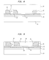
- FIGS 1 through 9 illustrate the process steps in the fabrication of a BiCMOS compatible bonded SOI structure in accordance with the teachings of this invention.
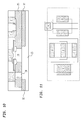
- Figures 10 and 11 show, respectively, a sectional view and a plan view of a BiCMOS device fabricated on an SOI structure constructed in accordance with the teachings of this invention.
- the process for this particular embodiment of the invention starts with an n-type, bulk, silicon wafer 10 with a doping concentration of approximately 1 X 10¹⁶ atoms/cm3.
- a wafer with a different doping concentration, and/or p-type doping could be used, depending on the final device requirements.
- a thin layer 12 (about 300 nm) of oxide/nitride composite film is deposited on the surface of the wafer 10 by a chemical vapor deposition (CVD) process and a resist 14 is then formed over the surface of the CVD oxide/nitride layer 12.
- CVD chemical vapor deposition
- the resist 14 is patterned and an opening in the oxide/nitride layer 12 is etched to form a reach-through opening through which an implant is made to form an n+ region 18.
- the n+ region 18 can be made by implanting arsenic or phosphorus ions so that after a bonding heat cycle the depth of the region is at least 0.5 ⁇ m.
- the device at this stage is shown in Figure 1.
- Trenches in the bulk silicon wafer 10 are next formed to define what will become relatively shallow and relatively deep semiconductor regions in the final structure.
- a SF6/Cl2 plasma is used to etch the trenches in the wafer 10.
- Trench segments are formed by an initial patterning of and etching through openings 23 in the resist 14, and openings in the layer 12.
- the bulk silicon wafer 10 is etched through these openings to a depth of less than 0.3 ⁇ m.
- Figure 2 illustrates this stage of the process. For shallow trenches, no further etching is needed.
- the openings 23 are enlarged with pattern and etched, and the trenches deepened to about 2.5 ⁇ m or less, thus forming a stepped trench with initially started trench segments 22 and those subsequently started segments indicated at 24 in Figure 3.
- the resist 14 is removed and a thin layer of oxide (not shown) is grown to passivate the trench sidewalls.
- the stepped trenches are filled with a suitable trench dielectric material 25 using a conventional shallow trench process; for example, depositing a TEOS layer (about 3.0 ⁇ m thick) by a CVD process step and planarizing the TEOS layer by a suitable chemical-mechanical polishing step to polish back to the upper surface of the oxide/nitride polish step layer 12. After polishing, the oxide/nitride layer 12 is removed.
- the device at this stage is shown in Figure 4.
- a polysilicon layer 26 is now formed by depositing polysilicon about 0.4 ⁇ m thick by CVD process step.
- the polysilicon layer 26 is patterned and implanted to form n+ and/or p+ sub-collectors and/or local interconnections in regions dictated by the requirements of the final device.
- a thermal oxide layer about 50 nm thick is grown on the surface of the layer 26 and a CVD nitride layer 28, also about 50 nm thick, is then formed on the oxide layer.
- This oxide/nitride layer is then patterned and etched back in order to define the sub-collector and interconnect regions indicated by the general reference numeral 29.
- the device at this stage is shown in Figure 5.
- the exposed regions 29 of the polysilicon layer 26 are recess etched to a depth of about 200 nm and a thermal oxide 32 is grown to consume all the exposed portions of the layer 26.
- the device at this stage is shown in Figure 6.
- the nitride layer 28 is used as a chemical-mechanical polish stop and the surface of oxide 32 is planarized by chemical-mechanical polishing.
- the device at this stage is shown in Figure 7.
- the structure shown in Figure 7 is then "flipped over" and bonded to a semiconductor wafer 34 whose upper surface has been oxidized to form oxide layer 36 as shown in Figure 8.
- a conventional bonding process may be used to bond the structure shown in Figure 7 to the oxide layer 36; for example, the assembly is subjected to a temperature in the range of 850°C to 1100°C, which will also activate the sub-collector dopants and perform a drive in operation for the reach-through region 18. Further details of this bonding step are set forth in C.
- a SOI structure with deep silicon regions 38 is in a range between 1 ⁇ m and 2.5 ⁇ m, shallow silicon regions 40 less than 300 nm deep, and reach-through region 18.
- Devices can be fabricated in these regions using conventional process steps dictated by the type or types of devices desired. For example, emitter, intrinsic base and collector can be built at region 38 and the extrinsic base can be built at region 40. Hereby, the base to collector junction capacitance can be very small.
- FIG 10 is a cross-sectional view of an exemplary BiCMOS structure; the layout of this BiCMOS structure is shown in Figure 11.
Landscapes
- Metal-Oxide And Bipolar Metal-Oxide Semiconductor Integrated Circuits (AREA)
- Element Separation (AREA)
- Thin Film Transistor (AREA)
Applications Claiming Priority (2)
| Application Number | Priority Date | Filing Date | Title |
|---|---|---|---|
| US900028 | 1986-08-25 | ||
| US90002892A | 1992-06-17 | 1992-06-17 |
Publications (1)
| Publication Number | Publication Date |
|---|---|
| EP0575283A2 true EP0575283A2 (fr) | 1993-12-22 |
Family
ID=25411875
Family Applications (1)
| Application Number | Title | Priority Date | Filing Date |
|---|---|---|---|
| EP93480074A Withdrawn EP0575283A2 (fr) | 1992-06-17 | 1993-06-15 | Dispositif semi-conducteur du type SOI pour circuits intégrés du type BICMOS |
Country Status (3)
| Country | Link |
|---|---|
| US (2) | US5521399A (fr) |
| EP (1) | EP0575283A2 (fr) |
| JP (1) | JPH0834261B2 (fr) |
Cited By (2)
| Publication number | Priority date | Publication date | Assignee | Title |
|---|---|---|---|---|
| CN1063580C (zh) * | 1994-07-26 | 2001-03-21 | 索尼公司 | 制造具有多层互连的半导体器件的方法 |
| US6235601B1 (en) | 1995-12-28 | 2001-05-22 | Philips Electronics North America Corporation | Method of manufacturing a self-aligned vertical bipolar transistor |
Families Citing this family (35)
| Publication number | Priority date | Publication date | Assignee | Title |
|---|---|---|---|---|
| JP2739018B2 (ja) * | 1992-10-21 | 1998-04-08 | 三菱電機株式会社 | 誘電体分離半導体装置及びその製造方法 |
| US5631495A (en) * | 1994-11-29 | 1997-05-20 | International Business Machines Corporation | High performance bipolar devices with plurality of base contact regions formed around the emitter layer |
| US5872733A (en) * | 1995-06-06 | 1999-02-16 | International Business Machines Corporation | Ramp-up rate control circuit for flash memory charge pump |
| KR100218668B1 (ko) * | 1996-12-14 | 1999-09-01 | 권혁준 | 바이폴라 소자의 컬랙터 장치 및 그 제조방법 |
| US5914280A (en) * | 1996-12-23 | 1999-06-22 | Harris Corporation | Deep trench etch on bonded silicon wafer |
| US6133608A (en) * | 1997-04-23 | 2000-10-17 | International Business Machines Corporation | SOI-body selective link method and apparatus |
| US6160292A (en) * | 1997-04-23 | 2000-12-12 | International Business Machines Corporation | Circuit and methods to improve the operation of SOI devices |
| US5894152A (en) * | 1997-06-18 | 1999-04-13 | International Business Machines Corporation | SOI/bulk hybrid substrate and method of forming the same |
| KR100281109B1 (ko) * | 1997-12-15 | 2001-03-02 | 김영환 | 에스오아이(soi)소자및그의제조방법 |
| US6348715B1 (en) | 1997-12-15 | 2002-02-19 | Lg Semicon Co., Ltd. | SOI (silicon on insulator) device |
| US6030860A (en) * | 1997-12-19 | 2000-02-29 | Advanced Micro Devices, Inc. | Elevated substrate formation and local interconnect integrated fabrication |
| US6258693B1 (en) | 1997-12-23 | 2001-07-10 | Integrated Device Technology, Inc. | Ion implantation for scalability of isolation in an integrated circuit |
| KR100252751B1 (ko) * | 1997-12-27 | 2000-04-15 | 김영환 | 반도체 소자 제조 방법 |
| US6410369B1 (en) | 1998-04-22 | 2002-06-25 | International Business Machines Corporation | Soi-body selective link method and apparatus |
| US6097056A (en) * | 1998-04-28 | 2000-08-01 | International Business Machines Corporation | Field effect transistor having a floating gate |
| KR100267013B1 (ko) * | 1998-05-27 | 2000-09-15 | 윤종용 | 반도체 장치 및 그의 제조 방법 |
| KR20000040104A (ko) | 1998-12-17 | 2000-07-05 | 김영환 | 실리콘 온 인슐레이터 웨이퍼의 제조방법 |
| US6534381B2 (en) * | 1999-01-08 | 2003-03-18 | Silicon Genesis Corporation | Method for fabricating multi-layered substrates |
| US6476445B1 (en) | 1999-04-30 | 2002-11-05 | International Business Machines Corporation | Method and structures for dual depth oxygen layers in silicon-on-insulator processes |
| US6403447B1 (en) | 1999-07-07 | 2002-06-11 | Elantec Semiconductor, Inc. | Reduced substrate capacitance high performance SOI process |
| US6372600B1 (en) * | 1999-08-30 | 2002-04-16 | Agere Systems Guardian Corp. | Etch stops and alignment marks for bonded wafers |
| JP2001230315A (ja) | 2000-02-17 | 2001-08-24 | Mitsubishi Electric Corp | 半導体装置およびその製造方法 |
| US6555874B1 (en) * | 2000-08-28 | 2003-04-29 | Sharp Laboratories Of America, Inc. | Method of fabricating high performance SiGe heterojunction bipolar transistor BiCMOS on a silicon-on-insulator substrate |
| JP2002141476A (ja) | 2000-11-07 | 2002-05-17 | Hitachi Ltd | BiCMOS半導体集積回路装置およびその製造方法 |
| US6294413B1 (en) * | 2000-12-27 | 2001-09-25 | Vanguard International Semiconductor Corp. | Method for fabricating a SOI (silicon on insulator) device |
| US6613652B2 (en) | 2001-03-14 | 2003-09-02 | Chartered Semiconductor Manufacturing Ltd. | Method for fabricating SOI devices with option of incorporating air-gap feature for better insulation and performance |
| US6468880B1 (en) | 2001-03-15 | 2002-10-22 | Chartered Semiconductor Manufacturing Ltd. | Method for fabricating complementary silicon on insulator devices using wafer bonding |
| US6566282B2 (en) * | 2001-06-21 | 2003-05-20 | United Microelectronics Corp. | Method of forming a silicon oxide layer |
| US7704542B2 (en) | 2001-09-12 | 2010-04-27 | Xanodyne Pharmaceuticals, Inc. | Vitamin/mineral compositions with DHA |
| US6936910B2 (en) * | 2003-05-09 | 2005-08-30 | International Business Machines Corporation | BiCMOS technology on SOI substrates |
| US20040222436A1 (en) * | 2003-05-09 | 2004-11-11 | International Business Machines Corporation | Bicmos technology on soi substrates |
| US7372091B2 (en) * | 2004-01-27 | 2008-05-13 | Micron Technology, Inc. | Selective epitaxy vertical integrated circuit components |
| US7504685B2 (en) | 2005-06-28 | 2009-03-17 | Micron Technology, Inc. | Oxide epitaxial isolation |
| US20070099372A1 (en) * | 2005-10-31 | 2007-05-03 | Sailesh Chittipeddi | Device having active regions of different depths |
| FR2993406B1 (fr) * | 2012-07-13 | 2014-08-22 | Commissariat Energie Atomique | Circuit integre sur soi comprenant un transistor bipolaire a tranchees d'isolation de profondeurs distinctes |
Family Cites Families (24)
| Publication number | Priority date | Publication date | Assignee | Title |
|---|---|---|---|---|
| US3913121A (en) * | 1963-12-16 | 1975-10-14 | Signetics Corp | Semiconductor structure |
| US3385729A (en) * | 1964-10-26 | 1968-05-28 | North American Rockwell | Composite dual dielectric for isolation in integrated circuits and method of making |
| JPS5779632A (en) * | 1980-11-05 | 1982-05-18 | Fujitsu Ltd | Manufacture of semiconductor device |
| JPS59182566A (ja) * | 1983-04-01 | 1984-10-17 | Hitachi Ltd | 半導体装置 |
| US4561172A (en) * | 1984-06-15 | 1985-12-31 | Texas Instruments Incorporated | Integrated circuit fabrication method utilizing selective etching and oxidation to form isolation regions |
| US4672410A (en) * | 1984-07-12 | 1987-06-09 | Nippon Telegraph & Telephone | Semiconductor memory device with trench surrounding each memory cell |
| JPH0715942B2 (ja) * | 1986-08-25 | 1995-02-22 | 日本電気株式会社 | 集積回路基板の製造方法 |
| JP2503460B2 (ja) * | 1986-12-01 | 1996-06-05 | 三菱電機株式会社 | バイポ−ラトランジスタおよびその製造方法 |
| JPS63202034A (ja) * | 1987-02-17 | 1988-08-22 | Mitsubishi Electric Corp | 半導体装置の製造方法 |
| JPS63205926A (ja) * | 1987-02-23 | 1988-08-25 | Nippon Telegr & Teleph Corp <Ntt> | 誘電体分離基板の製造方法 |
| US4897362A (en) * | 1987-09-02 | 1990-01-30 | Harris Corporation | Double epitaxial method of fabricating semiconductor devices on bonded wafers |
| US5298450A (en) * | 1987-12-10 | 1994-03-29 | Texas Instruments Incorporated | Process for simultaneously fabricating isolation structures for bipolar and CMOS circuits |
| JPH0239538A (ja) * | 1988-07-29 | 1990-02-08 | Sony Corp | 半導体装置とその製造方法 |
| JPH0739996B2 (ja) * | 1988-09-02 | 1995-05-01 | 日本電気株式会社 | 半田付検査装置 |
| JPH0276645A (ja) * | 1988-09-13 | 1990-03-16 | Honda Motor Co Ltd | ボルト締付装置 |
| JPH02125657A (ja) * | 1988-11-04 | 1990-05-14 | Fujitsu Ltd | 半導体装置 |
| US5164218A (en) * | 1989-05-12 | 1992-11-17 | Nippon Soken, Inc. | Semiconductor device and a method for producing the same |
| US4908328A (en) * | 1989-06-06 | 1990-03-13 | National Semiconductor Corporation | High voltage power IC process |
| JPH03123255A (ja) * | 1989-10-06 | 1991-05-27 | Nippondenso Co Ltd | 自動車用電話 |
| JPH03232239A (ja) * | 1990-02-07 | 1991-10-16 | Sharp Corp | 半導体装置の製造方法 |
| JPH03265155A (ja) * | 1990-03-15 | 1991-11-26 | Seiko Instr Inc | 半導体基板の製造方法 |
| JPH03265154A (ja) * | 1990-03-15 | 1991-11-26 | Nippon Soken Inc | 半導体基板の製造方法 |
| JPH0430449A (ja) * | 1990-05-25 | 1992-02-03 | Fuji Electric Co Ltd | 半導体集積装置の製造方法 |
| JP3014012B2 (ja) * | 1992-03-19 | 2000-02-28 | 日本電気株式会社 | 半導体装置の製造方法 |
-
1993
- 1993-06-04 JP JP5134747A patent/JPH0834261B2/ja not_active Expired - Fee Related
- 1993-06-15 EP EP93480074A patent/EP0575283A2/fr not_active Withdrawn
-
1994
- 1994-05-16 US US08/242,992 patent/US5521399A/en not_active Expired - Fee Related
-
1995
- 1995-03-01 US US08/396,985 patent/US5484738A/en not_active Expired - Fee Related
Cited By (2)
| Publication number | Priority date | Publication date | Assignee | Title |
|---|---|---|---|---|
| CN1063580C (zh) * | 1994-07-26 | 2001-03-21 | 索尼公司 | 制造具有多层互连的半导体器件的方法 |
| US6235601B1 (en) | 1995-12-28 | 2001-05-22 | Philips Electronics North America Corporation | Method of manufacturing a self-aligned vertical bipolar transistor |
Also Published As
| Publication number | Publication date |
|---|---|
| JPH06151727A (ja) | 1994-05-31 |
| JPH0834261B2 (ja) | 1996-03-29 |
| US5484738A (en) | 1996-01-16 |
| US5521399A (en) | 1996-05-28 |
Similar Documents
| Publication | Publication Date | Title |
|---|---|---|
| US5484738A (en) | Method of forming silicon on oxide semiconductor device structure for BiCMOS integrated circuits | |
| US4897362A (en) | Double epitaxial method of fabricating semiconductor devices on bonded wafers | |
| US6548364B2 (en) | Self-aligned SiGe HBT BiCMOS on SOI substrate and method of fabricating the same | |
| US5034338A (en) | Circuit containing integrated bipolar and complementary MOS transistors on a common substrate | |
| US6936910B2 (en) | BiCMOS technology on SOI substrates | |
| US5332920A (en) | Dielectrically isolated high and low voltage substrate regions | |
| US5512774A (en) | Dielectrically isolated substrate and semiconductor device using the same | |
| US4728624A (en) | Selective epitaxial growth structure and isolation | |
| US6897545B2 (en) | Lateral operation bipolar transistor and a corresponding fabrication process | |
| US6670255B2 (en) | Method of fabricating lateral diodes and bipolar transistors | |
| US6403447B1 (en) | Reduced substrate capacitance high performance SOI process | |
| US5395789A (en) | Integrated circuit with self-aligned isolation | |
| KR100487412B1 (ko) | 반도체 소자의 제조 방법 | |
| US6803642B2 (en) | Bipolar device having non-uniform depth base-emitter junction | |
| EP0045848B1 (fr) | Circuits intégrés semiconducteurs planaires comportant des structures de transistors bipolaires et procédé de fabrication correspondant | |
| US6153488A (en) | Method for producing semiconductor device, and semiconductor device produced by same | |
| US6087244A (en) | Methods of forming semiconductor-on-insulator devices including buried layers of opposite conductivity type | |
| US6972237B2 (en) | Lateral heterojunction bipolar transistor and method of manufacture using selective epitaxial growth | |
| US6140205A (en) | Method of forming retrograde well in bonded waffers | |
| US5616512A (en) | Power semiconductor devices | |
| KR101118649B1 (ko) | 바이폴라 트랜지스터 및 그 형성 방법 | |
| US5847438A (en) | Bonded IC substrate with a high breakdown voltage and large current capabilities | |
| JP3247106B2 (ja) | 集積回路の製法と集積回路構造 | |
| US6979624B2 (en) | Reduced mask count buried layer process | |
| US6830988B1 (en) | Method of forming an isolation structure for an integrated circuit utilizing grown and deposited oxide |
Legal Events
| Date | Code | Title | Description |
|---|---|---|---|
| PUAI | Public reference made under article 153(3) epc to a published international application that has entered the european phase |
Free format text: ORIGINAL CODE: 0009012 |
|
| AK | Designated contracting states |
Kind code of ref document: A2 Designated state(s): DE FR GB |
|
| 17P | Request for examination filed |
Effective date: 19940429 |
|
| STAA | Information on the status of an ep patent application or granted ep patent |
Free format text: STATUS: THE APPLICATION HAS BEEN WITHDRAWN |
|
| 18W | Application withdrawn |
Withdrawal date: 19960704 |