EP0410385A2 - Verfahren zur Herstellung eines Halbleiterbauelementes mit einem T-Gate - Google Patents
Verfahren zur Herstellung eines Halbleiterbauelementes mit einem T-Gate Download PDFInfo
- Publication number
- EP0410385A2 EP0410385A2 EP90114169A EP90114169A EP0410385A2 EP 0410385 A2 EP0410385 A2 EP 0410385A2 EP 90114169 A EP90114169 A EP 90114169A EP 90114169 A EP90114169 A EP 90114169A EP 0410385 A2 EP0410385 A2 EP 0410385A2
- Authority
- EP
- European Patent Office
- Prior art keywords
- resist layer
- aperture
- layer
- intermediate layer
- forming
- Prior art date
- Legal status (The legal status is an assumption and is not a legal conclusion. Google has not performed a legal analysis and makes no representation as to the accuracy of the status listed.)
- Granted
Links
Images




Classifications
-
- H—ELECTRICITY
- H10—SEMICONDUCTOR DEVICES; ELECTRIC SOLID-STATE DEVICES NOT OTHERWISE PROVIDED FOR
- H10D—INORGANIC ELECTRIC SEMICONDUCTOR DEVICES
- H10D30/00—Field-effect transistors [FET]
- H10D30/01—Manufacture or treatment
- H10D30/061—Manufacture or treatment of FETs having Schottky gates
- H10D30/0612—Manufacture or treatment of FETs having Schottky gates of lateral single-gate Schottky FETs
-
- H—ELECTRICITY
- H10—SEMICONDUCTOR DEVICES; ELECTRIC SOLID-STATE DEVICES NOT OTHERWISE PROVIDED FOR
- H10D—INORGANIC ELECTRIC SEMICONDUCTOR DEVICES
- H10D30/00—Field-effect transistors [FET]
- H10D30/80—FETs having rectifying junction gate electrodes
- H10D30/87—FETs having Schottky gate electrodes, e.g. metal-semiconductor FETs [MESFET]
-
- H—ELECTRICITY
- H10—SEMICONDUCTOR DEVICES; ELECTRIC SOLID-STATE DEVICES NOT OTHERWISE PROVIDED FOR
- H10D—INORGANIC ELECTRIC SEMICONDUCTOR DEVICES
- H10D64/00—Electrodes of devices having potential barriers
- H10D64/01—Manufacture or treatment
- H10D64/012—Manufacture or treatment of electrodes comprising a Schottky barrier to a semiconductor
- H10D64/0124—Manufacture or treatment of electrodes comprising a Schottky barrier to a semiconductor to Group III-V semiconductors
- H10D64/0125—Manufacture or treatment of electrodes comprising a Schottky barrier to a semiconductor to Group III-V semiconductors characterised by the sectional shape, e.g. T or inverted T
-
- Y—GENERAL TAGGING OF NEW TECHNOLOGICAL DEVELOPMENTS; GENERAL TAGGING OF CROSS-SECTIONAL TECHNOLOGIES SPANNING OVER SEVERAL SECTIONS OF THE IPC; TECHNICAL SUBJECTS COVERED BY FORMER USPC CROSS-REFERENCE ART COLLECTIONS [XRACs] AND DIGESTS
- Y10—TECHNICAL SUBJECTS COVERED BY FORMER USPC
- Y10S—TECHNICAL SUBJECTS COVERED BY FORMER USPC CROSS-REFERENCE ART COLLECTIONS [XRACs] AND DIGESTS
- Y10S148/00—Metal treatment
- Y10S148/10—Lift-off masking
-
- Y—GENERAL TAGGING OF NEW TECHNOLOGICAL DEVELOPMENTS; GENERAL TAGGING OF CROSS-SECTIONAL TECHNOLOGIES SPANNING OVER SEVERAL SECTIONS OF THE IPC; TECHNICAL SUBJECTS COVERED BY FORMER USPC CROSS-REFERENCE ART COLLECTIONS [XRACs] AND DIGESTS
- Y10—TECHNICAL SUBJECTS COVERED BY FORMER USPC
- Y10S—TECHNICAL SUBJECTS COVERED BY FORMER USPC CROSS-REFERENCE ART COLLECTIONS [XRACs] AND DIGESTS
- Y10S148/00—Metal treatment
- Y10S148/143—Shadow masking
Definitions
- the present invention relates to a method for manufacture of a semiconductor device and, more particularly, a semiconductor device wherein a T-shaped gate (mushroom-like gate) is formed on a substrate of a compound semiconductor or the like.
- the gate be formed so as to be sectionally T-shaped (mushroom-like) for reducing the gate resistance while shortening the length.
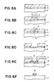
- FIGS. 8A through 8F are sectional views illustrating successive steps executed sequentially in a first conventional example of a method for forming such a T-shaped gate.
- FIG. 9 is a sectional view of a second conventional example achieved by partially modifying the T-shaped gate forming method illustrated in FIG. 8.
- a first resist layer b and a second resist layer c are sequentially formed on a substrate a , and the material of the first resist layer b is selected so as to be lower in sensitivity than that of the second resist layer c .
- the two resist layers b and c are exposed in a single process.
- An aperture is formed in the lower or first resist layer b which is smaller than an aperture in the upper or second resist layer c .
- a single exposure step is sufficient to attain this purpose since the respective sensitivities of the first resist layer b and the second resist layer c are different from each other.
- FIGS. 10A through 10E are sectional views illustrating successive steps sequentially in a third conventional example for forming the T-shaped gate.
- the present invention has been accomplished in view of the problems mentioned. Its object is to provide an improved method which is capable of easing the lift-off process required in forming a desired T-shaped gate and to thereby enhance the lift-off facility.
- an intermediate layer is interposed between the first and the second resist layers, and after the second resist layer is patterned to form an aperture therein, the intermediate layer is overetched through such aperture so that the first resist layer is under-cut, and subsequently the first resist layer is patterned, whereby the lift-off facility can be remarkably enhanced.
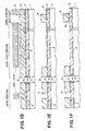
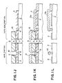
- FIGS. 1A through 1L are sectional views illustrating successive steps of a first exemplary embodiment to implement the semiconductor device manufacturing method of the present invention.
- a source electrode and a drain electrode (AuGe/Ni) 2 are selectively formed on the surface of a compound semiconductor substrate (e.g., GaAs substrate) 1.
- a reflecting film 3 of gold, chromium, titanium or the like is formed to a thickness less than 1000 angstroms in a portion where a mark is to be formed later.
- the requisite for the reflecting film 3 is merely to satisfy the condition that it can serve as a foundation for a positioning mark in an intermediate layer of aluminum or the like to be formed later above the reflecting film 3, and strict conditions are not required with regard to the pattern and the positional precision.
- the reflecting film 3 is provided for the purpose of attaining a sufficiently high intensity ratio between the reflected electrons (secondary electrons) in the mark and those in any other portion when a positioning step is later executed by detecting the position of the mark by the use of an electron beam. Therefore, in case a required high intensity ratio of the reflected electrons can be obtained without provision of the reflecting film 3, it is not absolutely necessary to form such film 3.
- the first resist layer 4 is of positive type (e.g., such as OEBR-1010 (trade name) made by Tokyo Applied Chemical Co., Ltd.) which is to be exposed by the use of an electron beam and has a thickness of 0.4 micron or so.
- positive type e.g., such as OEBR-1010 (trade name) made by Tokyo Applied Chemical Co., Ltd.
- the intermediate layer 5 is composed of aluminum, for example, and has a thickness of 1000 angstroms or so. As will be described in detail later, the intermediate layer 5 serves essentially to improve the lift-off facility and has, particularly in this embodiment, an additional role to shield the first resist layer 4 from exposure by intercepting the light at the time of exposure of the second resist layer 6. Furthermore, the intermediate layer 5 functions also as a positioning reference mark at the time of exposing the first resist layer 4 after patterning the second resist layer 6.
- the second resist layer 6 is of positive type (e.g., such as ODUR-1010 (trade name) made by Tokyo Applied Chemical Co., Ltd.) which is to be exposed by the use of DUV light and has a thickness of 1.2 micron or so.
- positive type e.g., such as ODUR-1010 (trade name) made by Tokyo Applied Chemical Co., Ltd.
- the first resist layer 6 is exposed to DUV light. Such exposure is selectively applied to a T-shaped gate forming region inclusive of a gate lead portion, but not to a mark portion in a mark forming region.
- the intermediate layer 5 serves as a shielding film to the DUV light, thereby positively preventing exposure of the first resist layer 4.
- the second resist layer 6 is developed to form an aperture 7 in the region where a T-shaped gate is to be formed. At the same time in the mark forming region, the second resist layer 6 is partially left in the portion which is to be used as a mark.
- the intermediate layer 5 is selectively removed by etching with a solution while masked with the second resist layer 6.
- a portion 5a of the intermediate layer 5 which is left unremoved due to the mask of the second resist layer 6 becomes a positioning mark.
- the first resist layer 4 is exposed by an electron beam.
- Such exposure is performed for opening a portion where the T-shaped gate is to be in contact with the substrate 1, and the exposed portion needs to be positioned inside of the aperture 7 and to be narrower than the aperture 7. It is necessary that high positional precision be attained between the exposed position and the aperture 7, and therefore the positioning is carried out with reference to the positioning mark 5a formed in the intermediate layer. Consequently, it becomes possible to ensure the required high positioning precision.
- the positioning mark 6 is not later used.
- the intermediate layer 5 serves to suppress charge-up of the exposed portion.
- the exposed portion of the resist layer is charged up, and a repulsive force is exerted on a new electron beam which is successively irradiated. Since such repulsive force is exerted so as to deviate the electron beam from its target point, there are induced some faults such as enlarging the exposed region and deteriorating the positional precision during the exposure.
- the charges in the exposed portion are ready to be dissipated by way of the intermediate layer 5 which is conductive and which is located in the vicinity of the exposed region.
- the intermediate layer 5 can serve effectively to suppress charge up.
- the intermediate layer 5 is over-etched through the aperture 7.
- This etching step is executed so as to produce a gap 8 (under-etched portion for the second resist layer 6) between the first resist layer 4 and the second resist layer 6.
- the amount of side etching is 1 micron or so. Due to the existence of such gap 8, the lift-off process to be carried out later is facilitated.
- the lower surface of the first resist layer 1 may be eroded as indicated by a broken line. Such eroded portion 10 serves to enhance the lift-off facility
- the surface of the substrate 1 is recess-etched with the second resist layer 4 used as a mask, so that the pinch-off voltage of the transistor is lowered.
- the recess-etched portion 11 is shown in FIG. 1J.
- a film 12 having a thickness of 5000 angstroms or so is formed by evaporating a suitable gate material such as aluminum. This step may be executed by oblique evaporation of the source-side offset or by evaporation without any offset.
- a T-shaped gate 13 is formed in the aperture of the first resist layer 4.
- Reference numeral 13a denotes a lead portion of the T-shaped gate 13.
- the lead portion 13a of the T-shaped gate 13 is formed so as to be astride a source electrode or a drain region like an air bridge.
- FIG. 2 is a plan view behind the T-shaped gate.
- the gate portion illustrated in FIGS. 1A through 1L corresponds to a view taken along the line A-A in FIG. 2, and the gate lead portion in FIG. 1 corresponds to a view taken along the line B-B in FIG. 2.
- FIG. 3 is a sectional view taken along the line C-C in FIG. 2, wherein reference numeral 14 denotes a passivation film. Since film 14 is formed after completion of the T-shaped gate 13, it is not shown in FIG. 1.
- a space 15 is enclosed by the T-shaped gate 13, the gate lead portion 13a, the electrode 2 and the passivation film 14.
- the space 15 is filled with air. In this structure, it becomes possible to reduce the parasitic capacitance between the gate and the substrate, since air has a minimum dielectric constant.
- the gate is led out using an air bridge mode.
- the first and second resist layers are formed with the intermediate layer interposed therebetween, and the first resist layer can be utilized as a space between the gate lead portion 13a and the substrate 1.
- the gate can be led out without the necessity of any additional step for forming a lead portion alone.
- FIG. 4 is a plan view illustrating the simplest leading means, wherein either a source electrode 2 or a drain electrode 2 is divided, and a lead portion 13a of a T-shaped gate 13 is inserted into a space between the divided electrode portions.
- FIG. 5 is a plan view of a semiconductor device constructed to solve the above problem.
- a lead portion 13a of a T-shaped gate 13 is formed like an air bridge.
- the lead portion 13a of the T-shaped gate 13 is formed so as to pass over, for example, a source electrode 2.
- the T-shaped gate 13 and its lead portion 13a are individually formed during different steps, which increases the number of required steps.
- the lead portion 13a is formed after completion of ther T-shaped gate 13.
- some additional problems arise with regard to the positioning difficulty and the increase of the gate resistance due to the existence of contact resistance between the T-shaped gate 13 and the lead portion 13a.
- the positioning mark 5a is formed from the intermediate layer 5, and such mark 5a is used as a positioning reference during the step of exposing the first resist layer 4.
- the procedure is not only limited thereto.
- the step of exposing the second resist layer 4 and the step of over-etching the intermediate layer 5 may be reversed in order. That is, instead of over-etching the intermediate layer 5 after termination of the exposure, the second resist layer 4 may be exposed after completion of over-etching the intermediate layer 5.
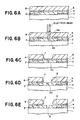
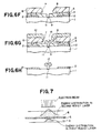
- FIGS. 6A through 6H are sectional views illustrating successive steps of a second exemplary embodiment to implement the semiconductor device manufacturing method of the present invention.
- a first resist layer 4, an intermediate layer 5 and a second resist layer 6 are sequentially formed after the completion of forming a source electrode and a drain electrode 2 on a substrate 1.
- the first resist layer 4 is of positive type such as (e.g., OEBR-1010) (trade name) made by Tokyo Applied Chemical Co., Ltd.) which is to be exposed by the use of an electron beam and has a thickness of 0.3 micron or so.
- the intermediate layer 5 is composed of aluminum, for example, and has a thickness of 1000 angstroms or so.
- the second resist layer 6 is of positive type such as (e.g., OEBR-1010 (trade name) made by Tokyo Applied Chemical Co., Ltd.) which is to be exposed by the use of an electron beam similarly to the first resist layer 4, and it has a thickness of 0.6 micron or so.
- positive type such as (e.g., OEBR-1010 (trade name) made by Tokyo Applied Chemical Co., Ltd.) which is to be exposed by the use of an electron beam similarly to the first resist layer 4, and it has a thickness of 0.6 micron or so.
- the first and second resist layers may have the same characteristics in this embodiment, or may have different ones as well. However, it is not preferable that the sensitivity of the second resist layer be lower than that of the first resist layer, because an aperture formed in the first resist layer needs to be definitely smaller than an aperture formed in the second resist layer.
- the thickness of the intermediate layer 5 is merely 0.1 micron or so, the light shielding effect thereof is not retained, so that the first resist layer 4 is also exposed by the electron beam through the intermediate layer 5 in addition to the second resist layer 6.
- DUV light is employed for exposure of the second resist layer 6 as mentioned, and the intermediate layer 5 serves as a light shielding film thereto.
- the electron beam for exposure is permitted to pass through the intermediate layer 5, thereby exposing the first resist layer 4 simultaneously with the second resist layer 6.
- An aperture to be formed in the first resist layer 4 needs to be smaller than an aperture in the second resist layer 6. Since the intermediate layer 5 has a filter effect as illustrated in FIG. 7, the area of the exposed portion of the first resist layer 4 is reduced so as to be less than the area of the exposed portion of the second resist layer 6, which results in the desired dimensional relationship between the first resist layer 4 and the second resist layer 6. That is, in the first resist layer 5 where the energy of the irradiated electron beam is distributed through the intermediate layer 5, the energy distribution is made narrower than that in the second resist layer 6. Therefore, it becomes possible to reduce the exposed portion area of the first resist layer 4 so that it is smaller than that of the second resist layer 6.
- the intermediate layer 5 is over-etched to define a gap 8 between the first resist layer 4 and the second resist layer 6.
- gap 8 is effective to enhance the lift-off facility.
- the first resist layer 4 is developed to form an aperture 9.
- the second resist layer 6 is somewhat eroded so that the aperture 7 therein is made slightly larger than the aperture 9, whereby the lift-off facility is further enhanced.
- the surface of the substrate 1 is recess-etched while the first resist layer 4 is used as a mask.
- a recess-etched portion 11 is illustrated.
- a film 12 is formed by evaporating a suitable gate material (such as aluminum), so that a T-shaped gate 13 is formed in the aperture 9 of the first resist layer 4.
- a suitable gate material such as aluminum
- the lift-off facility is enhanced due to the under-cut portion 8 produced for the second resist layer 6 by over-etching the intermediate layer 5 and also due to the rounded or narrowed contour of the second resist layer 6 caused by the development of the first resist layer 4. Consequently, the lift-off operation can be smoothly performed.
- the intermediate layer 5 is effective to suppress the charge-up during the step of exposure.
- the intermediate layer 5 in this embodiment is composed of aluminum, the material is not limited to such material, and it need not be metallic.
- the intermediate layer 5 may be composed of an insulator film as well.
- any material is usable which can meet the requirements for the intermediate layer. Such condition is also applicable to the first embodiment.
- the intermediate layer 5 is composed of an insulator material, the effect of preventing the charge-up is not obtained.
- the step of exposure for forming a T-shaped gate can be completed with a single tracing movement of an electron beam, and it is not necessary to repeat the exposure as required in the first embodiment. In addition, the positioning between such repeated exposures is no longer necessary which increases the output.
- the size of the aperture 7 in the second resist layer 6 can be controlled by adjusting the time for developing the second resist layer 6, and the first resist layer 4 can be completely masked with the intermediate layer 5 during such development.
- the size of the aperture 9 in the first resist layer 4 and that of the aperture 7 in the second resist layer 6 are independently controllable of each other.
- the features of the semiconductor device manufacturing method of the present invention comprise executing successive steps of sequentially forming a first resist layer, an intermediate layer and a second resist layer on a substrate, then forming an aperture by removing a portion of the second resist layer where a T-shaped gate is to be later formed. Then subsequently over-etching the intermediate layer portion opposed to such aperture, thereby forming in the intermediate layer an aperture larger than the first-mentioned aperture, and thereafter forming in the first resist layer another aperture which is smaller than the aperture in the second resist layer and which is positioned inside thereof.
- the intermediate layer is interposed between the first and second resist layers and, after the second resist layer is patterned, the intermediate layer is over-etched through the aperture formed by such patterning, so that the first resist layer is under-cut. Thereafter the first resist layer is patterned to consequently attain substantial enhancement of the lift-off facility.
Landscapes
- Junction Field-Effect Transistors (AREA)
- Electron Beam Exposure (AREA)
- Exposure Of Semiconductors, Excluding Electron Or Ion Beam Exposure (AREA)
- Electrodes Of Semiconductors (AREA)
Applications Claiming Priority (2)
| Application Number | Priority Date | Filing Date | Title |
|---|---|---|---|
| JP1192854A JPH0355852A (ja) | 1989-07-25 | 1989-07-25 | 半導体装置の製造方法 |
| JP192854/89 | 1989-07-25 |
Publications (3)
| Publication Number | Publication Date |
|---|---|
| EP0410385A2 true EP0410385A2 (de) | 1991-01-30 |
| EP0410385A3 EP0410385A3 (en) | 1991-05-02 |
| EP0410385B1 EP0410385B1 (de) | 1995-12-06 |
Family
ID=16298077
Family Applications (1)
| Application Number | Title | Priority Date | Filing Date |
|---|---|---|---|
| EP90114169A Expired - Lifetime EP0410385B1 (de) | 1989-07-25 | 1990-07-24 | Verfahren zur Herstellung eines Halbleiterbauelementes mit einem T-Gate |
Country Status (5)
| Country | Link |
|---|---|
| US (1) | US5006478A (de) |
| EP (1) | EP0410385B1 (de) |
| JP (1) | JPH0355852A (de) |
| KR (1) | KR910003752A (de) |
| DE (1) | DE69023976T2 (de) |
Cited By (6)
| Publication number | Priority date | Publication date | Assignee | Title |
|---|---|---|---|---|
| FR2663155A1 (fr) * | 1990-06-12 | 1991-12-13 | Thomson Composants Microondes | Procede de realisation d'une grille de transistor. |
| US5288660A (en) * | 1993-02-01 | 1994-02-22 | Avantek, Inc. | Method for forming self-aligned t-shaped transistor electrode |
| EP0591608A3 (de) * | 1992-09-29 | 1995-01-25 | Mitsubishi Electric Corp | Verfahren zum Herstellung einer T-förmigen Gatten-Elektrode in einem Halbleiterbauelement. |
| EP0724288A3 (de) * | 1995-01-30 | 1996-08-21 | Honda Motor Co Ltd | |
| US5583063A (en) * | 1993-11-30 | 1996-12-10 | Nec Corporation | Method of forming T-shaped, cross-sectional pattern using two layered masks |
| US20110180850A1 (en) * | 2010-01-25 | 2011-07-28 | Ishiang Shih | Configuration and manufacturing method of low-resistance gate structures for semiconductor devices and circuits |
Families Citing this family (29)
| Publication number | Priority date | Publication date | Assignee | Title |
|---|---|---|---|---|
| JPH03248439A (ja) * | 1990-02-26 | 1991-11-06 | Rohm Co Ltd | 化合物半導体装置の製造方法 |
| JPH04130619A (ja) * | 1990-09-20 | 1992-05-01 | Mitsubishi Electric Corp | 半導体装置の製造方法 |
| JPH04155835A (ja) * | 1990-10-18 | 1992-05-28 | Mitsubishi Electric Corp | 集積回路装置の製造方法 |
| US5185278A (en) * | 1990-10-22 | 1993-02-09 | Motorola, Inc. | Method of making self-aligned gate providing improved breakdown voltage |
| JPH0575139A (ja) * | 1991-09-12 | 1993-03-26 | Mitsubishi Electric Corp | 半導体装置及びその製造方法 |
| US5328868A (en) * | 1992-01-14 | 1994-07-12 | International Business Machines Corporation | Method of forming metal connections |
| EP0642175B1 (de) * | 1993-09-07 | 2004-04-28 | Murata Manufacturing Co., Ltd. | Halbleiteranordnung mit Schottky-Elektrode und Verfahren zur Herstellung |
| JP2725592B2 (ja) * | 1994-03-30 | 1998-03-11 | 日本電気株式会社 | 電界効果トランジスタの製造方法 |
| US5824575A (en) * | 1994-08-22 | 1998-10-20 | Matsushita Electric Industrial Co., Ltd. | Semiconductor device and method of manufacturing the same |
| US5486483A (en) * | 1994-09-27 | 1996-01-23 | Trw Inc. | Method of forming closely spaced metal electrodes in a semiconductor device |
| JPH08111424A (ja) * | 1994-10-11 | 1996-04-30 | Mitsubishi Electric Corp | 半導体装置の製造方法 |
| US5693548A (en) * | 1994-12-19 | 1997-12-02 | Electronics And Telecommunications Research Institute | Method for making T-gate of field effect transistor |
| US5733827A (en) * | 1995-11-13 | 1998-03-31 | Motorola, Inc. | Method of fabricating semiconductor devices with a passivated surface |
| JP3332851B2 (ja) * | 1998-04-22 | 2002-10-07 | 松下電器産業株式会社 | 半導体装置の製造方法 |
| US6270929B1 (en) * | 2000-07-20 | 2001-08-07 | Advanced Micro Devices, Inc. | Damascene T-gate using a relacs flow |
| US7008832B1 (en) | 2000-07-20 | 2006-03-07 | Advanced Micro Devices, Inc. | Damascene process for a T-shaped gate electrode |
| US6524937B1 (en) * | 2000-08-23 | 2003-02-25 | Tyco Electronics Corp. | Selective T-gate process |
| JP4093395B2 (ja) * | 2001-08-03 | 2008-06-04 | 富士通株式会社 | 半導体装置とその製造方法 |
| WO2006007192A2 (en) * | 2004-05-27 | 2006-01-19 | University Of Delaware | Three-dimensional photoresist structures and method of making |
| US8981876B2 (en) | 2004-11-15 | 2015-03-17 | Avago Technologies General Ip (Singapore) Pte. Ltd. | Piezoelectric resonator structures and electrical filters having frame elements |
| US20080305442A1 (en) * | 2007-06-05 | 2008-12-11 | Tdk Corporation | Patterned material layer, method of forming the same, microdevice, and method of manufacturing the same |
| US9243316B2 (en) | 2010-01-22 | 2016-01-26 | Avago Technologies General Ip (Singapore) Pte. Ltd. | Method of fabricating piezoelectric material with selected c-axis orientation |
| US8796904B2 (en) | 2011-10-31 | 2014-08-05 | Avago Technologies General Ip (Singapore) Pte. Ltd. | Bulk acoustic resonator comprising piezoelectric layer and inverse piezoelectric layer |
| US8962443B2 (en) | 2011-01-31 | 2015-02-24 | Avago Technologies General Ip (Singapore) Pte. Ltd. | Semiconductor device having an airbridge and method of fabricating the same |
| US9401692B2 (en) | 2012-10-29 | 2016-07-26 | Avago Technologies General Ip (Singapore) Pte. Ltd. | Acoustic resonator having collar structure |
| US9490771B2 (en) | 2012-10-29 | 2016-11-08 | Avago Technologies General Ip (Singapore) Pte. Ltd. | Acoustic resonator comprising collar and frame |
| US9490418B2 (en) | 2011-03-29 | 2016-11-08 | Avago Technologies General Ip (Singapore) Pte. Ltd. | Acoustic resonator comprising collar and acoustic reflector with temperature compensating layer |
| US9385684B2 (en) | 2012-10-23 | 2016-07-05 | Avago Technologies General Ip (Singapore) Pte. Ltd. | Acoustic resonator having guard ring |
| US9728444B2 (en) * | 2015-12-31 | 2017-08-08 | International Business Machines Corporation | Reactive ion etching assisted lift-off processes for fabricating thick metallization patterns with tight pitch |
Family Cites Families (15)
| Publication number | Priority date | Publication date | Assignee | Title |
|---|---|---|---|---|
| US3874916A (en) * | 1972-06-23 | 1975-04-01 | Radiant Energy Systems | Mask alignment system for electron beam pattern generator |
| US3994758A (en) * | 1973-03-19 | 1976-11-30 | Nippon Electric Company, Ltd. | Method of manufacturing a semiconductor device having closely spaced electrodes by perpendicular projection |
| US4283483A (en) * | 1979-07-19 | 1981-08-11 | Hughes Aircraft Company | Process for forming semiconductor devices using electron-sensitive resist patterns with controlled line profiles |
| JPS5811512B2 (ja) * | 1979-07-25 | 1983-03-03 | 超エル・エス・アイ技術研究組合 | パタ−ン形成方法 |
| JPS56133876A (en) * | 1980-03-24 | 1981-10-20 | Nippon Telegr & Teleph Corp <Ntt> | Manufacture of junction type field effect semiconductor device |
| US4440804A (en) * | 1982-08-02 | 1984-04-03 | Fairchild Camera & Instrument Corporation | Lift-off process for fabricating self-aligned contacts |
| JPS59141222A (ja) * | 1983-01-31 | 1984-08-13 | Matsushita Electric Ind Co Ltd | 半導体装置の製造方法 |
| JPS59232423A (ja) * | 1983-06-15 | 1984-12-27 | Matsushita Electric Ind Co Ltd | パタ−ン形成方法 |
| GB2156579B (en) * | 1984-03-15 | 1987-05-07 | Standard Telephones Cables Ltd | Field effect transistors |
| JPS60231331A (ja) * | 1984-04-27 | 1985-11-16 | Fujitsu Ltd | リフトオフ・パタ−ンの形成方法 |
| US4618510A (en) * | 1984-09-05 | 1986-10-21 | Hewlett Packard Company | Pre-passivated sub-micrometer gate electrodes for MESFET devices |
| IT1184723B (it) * | 1985-01-28 | 1987-10-28 | Telettra Lab Telefon | Transistore mesfet con strato d'aria tra le connessioni dell'elettrodo di gate al supporto e relativo procedimento difabbricazione |
| US4599790A (en) * | 1985-01-30 | 1986-07-15 | Texas Instruments Incorporated | Process for forming a T-shaped gate structure |
| IT1190294B (it) * | 1986-02-13 | 1988-02-16 | Selenia Ind Elettroniche | Una struttura di fotopolimero a multistrati (mlr) per la fabbricazione di dispositivi mesfet con gate submicrometrico e con canale incassato (recesse) di lunghezza variabile |
| EP0332680B1 (de) * | 1987-09-14 | 1993-12-01 | Hughes Aircraft Company | Verfahren zur herstellung einer t-gate metallstruktur auf einem substrat |
-
1989
- 1989-07-25 JP JP1192854A patent/JPH0355852A/ja active Pending
-
1990
- 1990-07-24 EP EP90114169A patent/EP0410385B1/de not_active Expired - Lifetime
- 1990-07-24 US US07/556,480 patent/US5006478A/en not_active Expired - Fee Related
- 1990-07-24 DE DE69023976T patent/DE69023976T2/de not_active Expired - Fee Related
- 1990-07-24 KR KR1019900011235A patent/KR910003752A/ko not_active Ceased
Cited By (9)
| Publication number | Priority date | Publication date | Assignee | Title |
|---|---|---|---|---|
| FR2663155A1 (fr) * | 1990-06-12 | 1991-12-13 | Thomson Composants Microondes | Procede de realisation d'une grille de transistor. |
| EP0466527A3 (en) * | 1990-06-12 | 1992-05-20 | Thomson Composants Microondes | Process for manufacturing the gate of a transistor |
| US5185277A (en) * | 1990-06-12 | 1993-02-09 | Thomson Composants Microondes | Method for the making of a transistor gate |
| EP0591608A3 (de) * | 1992-09-29 | 1995-01-25 | Mitsubishi Electric Corp | Verfahren zum Herstellung einer T-förmigen Gatten-Elektrode in einem Halbleiterbauelement. |
| US5288660A (en) * | 1993-02-01 | 1994-02-22 | Avantek, Inc. | Method for forming self-aligned t-shaped transistor electrode |
| US5583063A (en) * | 1993-11-30 | 1996-12-10 | Nec Corporation | Method of forming T-shaped, cross-sectional pattern using two layered masks |
| EP0724288A3 (de) * | 1995-01-30 | 1996-08-21 | Honda Motor Co Ltd | |
| US20110180850A1 (en) * | 2010-01-25 | 2011-07-28 | Ishiang Shih | Configuration and manufacturing method of low-resistance gate structures for semiconductor devices and circuits |
| US8283221B2 (en) * | 2010-01-25 | 2012-10-09 | Ishiang Shih | Configuration and manufacturing method of low-resistance gate structures for semiconductor devices and circuits |
Also Published As
| Publication number | Publication date |
|---|---|
| EP0410385A3 (en) | 1991-05-02 |
| US5006478A (en) | 1991-04-09 |
| DE69023976D1 (de) | 1996-01-18 |
| KR910003752A (ko) | 1991-02-28 |
| JPH0355852A (ja) | 1991-03-11 |
| EP0410385B1 (de) | 1995-12-06 |
| DE69023976T2 (de) | 1996-07-18 |
Similar Documents
| Publication | Publication Date | Title |
|---|---|---|
| US5006478A (en) | Method for manufacture of semiconductor device | |
| US4109029A (en) | High resolution electron beam microfabrication process for fabricating small geometry semiconductor devices | |
| KR0130963B1 (ko) | T형 단면구조의 게이트 금속전극을 갖는 전계효과 트랜지스터의 제조방법 | |
| US4694564A (en) | Method for the manufacture of a Schottky gate field effect transistor | |
| US20040032031A1 (en) | Use of a dual-tone resist to form photomasks including alignment mark protection, intermediate semiconductor device structures and bulk semiconductor device substrates | |
| US4975382A (en) | Method of making a self-aligned field-effect transistor by the use of a dummy-gate | |
| US5139968A (en) | Method of producing a t-shaped gate electrode | |
| JP2560993B2 (ja) | 化合物半導体装置の製造方法 | |
| JPH07176544A (ja) | 半導体装置およびその製造方法 | |
| US4935377A (en) | Method of fabricating microwave FET having gate with submicron length | |
| US5260599A (en) | Conductive clearing frame for a semiconductor component | |
| EP0385031B1 (de) | Halbleiteranordnung mit einem eingefügten Gate und Verfahren zur Herstellung | |
| US6383853B2 (en) | Method of fabricating semiconductor device | |
| EP0978869A2 (de) | Verfahren zur Herstellung eines kleinen Resistmusters sowie Verfahren zur Herstellung einer Gateelektrode | |
| US4939071A (en) | Method for forming low resistance, sub-micrometer semiconductor gate structures | |
| JP2714026B2 (ja) | 半導体装置用電極の形成方法 | |
| JPH06260509A (ja) | 半導体装置の製造方法 | |
| US5407859A (en) | Field effect transistor with landing pad | |
| JPS5838945B2 (ja) | シヨット障壁型電界効果トランジスタの製造方法 | |
| JPH07193088A (ja) | 電界効果トランジスタの製造方法 | |
| JP2962262B2 (ja) | 微細ゲート電極の形成方法 | |
| JPH07240425A (ja) | 半導体装置の製造方法 | |
| JPS61245581A (ja) | 半導体装置の製造方法 | |
| JPH0462938A (ja) | 半導体装置の製造方法 | |
| JPH0831844A (ja) | 半導体装置の製造方法 |
Legal Events
| Date | Code | Title | Description |
|---|---|---|---|
| PUAI | Public reference made under article 153(3) epc to a published international application that has entered the european phase |
Free format text: ORIGINAL CODE: 0009012 |
|
| AK | Designated contracting states |
Kind code of ref document: A2 Designated state(s): DE FR GB |
|
| 17P | Request for examination filed |
Effective date: 19901220 |
|
| PUAL | Search report despatched |
Free format text: ORIGINAL CODE: 0009013 |
|
| AK | Designated contracting states |
Kind code of ref document: A3 Designated state(s): DE FR GB |
|
| 17Q | First examination report despatched |
Effective date: 19930521 |
|
| GRAA | (expected) grant |
Free format text: ORIGINAL CODE: 0009210 |
|
| AK | Designated contracting states |
Kind code of ref document: B1 Designated state(s): DE FR GB |
|
| REF | Corresponds to: |
Ref document number: 69023976 Country of ref document: DE Date of ref document: 19960118 |
|
| ET | Fr: translation filed | ||
| PGFP | Annual fee paid to national office [announced via postgrant information from national office to epo] |
Ref country code: GB Payment date: 19960715 Year of fee payment: 7 |
|
| PGFP | Annual fee paid to national office [announced via postgrant information from national office to epo] |
Ref country code: DE Payment date: 19960802 Year of fee payment: 7 |
|
| PLBE | No opposition filed within time limit |
Free format text: ORIGINAL CODE: 0009261 |
|
| STAA | Information on the status of an ep patent application or granted ep patent |
Free format text: STATUS: NO OPPOSITION FILED WITHIN TIME LIMIT |
|
| 26N | No opposition filed | ||
| PG25 | Lapsed in a contracting state [announced via postgrant information from national office to epo] |
Ref country code: GB Free format text: LAPSE BECAUSE OF NON-PAYMENT OF DUE FEES Effective date: 19970724 |
|
| GBPC | Gb: european patent ceased through non-payment of renewal fee |
Effective date: 19970724 |
|
| PG25 | Lapsed in a contracting state [announced via postgrant information from national office to epo] |
Ref country code: DE Free format text: LAPSE BECAUSE OF NON-PAYMENT OF DUE FEES Effective date: 19980401 |
|
| PGFP | Annual fee paid to national office [announced via postgrant information from national office to epo] |
Ref country code: FR Payment date: 20020709 Year of fee payment: 13 |
|
| PG25 | Lapsed in a contracting state [announced via postgrant information from national office to epo] |
Ref country code: FR Free format text: LAPSE BECAUSE OF NON-PAYMENT OF DUE FEES Effective date: 20040331 |
|
| REG | Reference to a national code |
Ref country code: FR Ref legal event code: ST |