EP0418833A2 - Film mince organique et dispositif d'affichage à cristal liquide le comportant - Google Patents
Film mince organique et dispositif d'affichage à cristal liquide le comportant Download PDFInfo
- Publication number
- EP0418833A2 EP0418833A2 EP90117959A EP90117959A EP0418833A2 EP 0418833 A2 EP0418833 A2 EP 0418833A2 EP 90117959 A EP90117959 A EP 90117959A EP 90117959 A EP90117959 A EP 90117959A EP 0418833 A2 EP0418833 A2 EP 0418833A2
- Authority
- EP
- European Patent Office
- Prior art keywords
- thin film
- film
- liquid crystal
- organic thin
- organic
- Prior art date
- Legal status (The legal status is an assumption and is not a legal conclusion. Google has not performed a legal analysis and makes no representation as to the accuracy of the status listed.)
- Withdrawn
Links
- 239000010409 thin film Substances 0.000 title claims abstract description 231
- 239000004973 liquid crystal related substance Substances 0.000 title claims abstract description 153
- 239000010408 film Substances 0.000 claims abstract description 251
- 239000000758 substrate Substances 0.000 claims abstract description 116
- 229920000642 polymer Polymers 0.000 claims abstract description 103
- 239000000126 substance Substances 0.000 claims abstract description 66
- 239000007788 liquid Substances 0.000 claims abstract description 52
- 230000006835 compression Effects 0.000 claims abstract description 37
- 238000007906 compression Methods 0.000 claims abstract description 37
- 239000004065 semiconductor Substances 0.000 claims abstract description 15
- 230000007480 spreading Effects 0.000 claims abstract description 10
- 238000003892 spreading Methods 0.000 claims abstract description 10
- 238000000034 method Methods 0.000 claims description 121
- 229920000015 polydiacetylene Polymers 0.000 claims description 38
- 238000004519 manufacturing process Methods 0.000 claims description 34
- 239000000203 mixture Substances 0.000 claims description 31
- 239000002243 precursor Substances 0.000 claims description 29
- 125000001424 substituent group Chemical group 0.000 claims description 26
- 239000000243 solution Substances 0.000 claims description 21
- 238000001228 spectrum Methods 0.000 claims description 19
- 150000001875 compounds Chemical class 0.000 claims description 18
- 238000007598 dipping method Methods 0.000 claims description 18
- 238000001771 vacuum deposition Methods 0.000 claims description 16
- LLCSWKVOHICRDD-UHFFFAOYSA-N buta-1,3-diyne Chemical group C#CC#C LLCSWKVOHICRDD-UHFFFAOYSA-N 0.000 claims description 14
- 239000000975 dye Substances 0.000 claims description 14
- 239000004988 Nematic liquid crystal Substances 0.000 claims description 13
- 125000000217 alkyl group Chemical group 0.000 claims description 12
- 230000015572 biosynthetic process Effects 0.000 claims description 12
- -1 polyethylene Polymers 0.000 claims description 12
- 238000000151 deposition Methods 0.000 claims description 11
- 239000003960 organic solvent Substances 0.000 claims description 11
- IEQIEDJGQAUEQZ-UHFFFAOYSA-N phthalocyanine Chemical class N1C(N=C2C3=CC=CC=C3C(N=C3C4=CC=CC=C4C(=N4)N3)=N2)=C(C=CC=C2)C2=C1N=C1C2=CC=CC=C2C4=N1 IEQIEDJGQAUEQZ-UHFFFAOYSA-N 0.000 claims description 11
- 229920001721 polyimide Polymers 0.000 claims description 11
- 238000000862 absorption spectrum Methods 0.000 claims description 10
- 125000005678 ethenylene group Chemical group [H]C([*:1])=C([H])[*:2] 0.000 claims description 10
- 239000000463 material Substances 0.000 claims description 10
- 230000003287 optical effect Effects 0.000 claims description 10
- 150000002894 organic compounds Chemical class 0.000 claims description 10
- 238000005266 casting Methods 0.000 claims description 9
- 239000007787 solid Substances 0.000 claims description 9
- HSFWRNGVRCDJHI-UHFFFAOYSA-N alpha-acetylene Natural products C#C HSFWRNGVRCDJHI-UHFFFAOYSA-N 0.000 claims description 8
- 230000008021 deposition Effects 0.000 claims description 8
- 238000010884 ion-beam technique Methods 0.000 claims description 8
- 230000009021 linear effect Effects 0.000 claims description 8
- 229920000553 poly(phenylenevinylene) Polymers 0.000 claims description 8
- 229920006254 polymer film Polymers 0.000 claims description 8
- 238000005507 spraying Methods 0.000 claims description 8
- 230000005684 electric field Effects 0.000 claims description 7
- 238000001451 molecular beam epitaxy Methods 0.000 claims description 7
- 229920000128 polypyrrole Polymers 0.000 claims description 7
- 230000001105 regulatory effect Effects 0.000 claims description 7
- 125000001140 1,4-phenylene group Chemical group [H]C1=C([H])C([*:2])=C([H])C([H])=C1[*:1] 0.000 claims description 6
- CQXXYOLFJXSRMT-UHFFFAOYSA-N 5-diazocyclohexa-1,3-diene Chemical class [N-]=[N+]=C1CC=CC=C1 CQXXYOLFJXSRMT-UHFFFAOYSA-N 0.000 claims description 6
- VGGSQFUCUMXWEO-UHFFFAOYSA-N Ethene Chemical class C=C VGGSQFUCUMXWEO-UHFFFAOYSA-N 0.000 claims description 6
- 239000000470 constituent Substances 0.000 claims description 6
- 229920000548 poly(silane) polymer Polymers 0.000 claims description 6
- 229920001197 polyacetylene Polymers 0.000 claims description 6
- 125000002887 hydroxy group Chemical group [H]O* 0.000 claims description 5
- NBIIXXVUZAFLBC-UHFFFAOYSA-N Phosphoric acid Chemical group OP(O)(O)=O NBIIXXVUZAFLBC-UHFFFAOYSA-N 0.000 claims description 4
- 239000004698 Polyethylene Substances 0.000 claims description 4
- 239000004990 Smectic liquid crystal Substances 0.000 claims description 4
- 150000000475 acetylene derivatives Chemical class 0.000 claims description 4
- 125000003277 amino group Chemical group 0.000 claims description 4
- 238000005229 chemical vapour deposition Methods 0.000 claims description 4
- 238000004070 electrodeposition Methods 0.000 claims description 4
- 238000001704 evaporation Methods 0.000 claims description 4
- 239000005262 ferroelectric liquid crystals (FLCs) Substances 0.000 claims description 4
- 238000007733 ion plating Methods 0.000 claims description 4
- 238000005268 plasma chemical vapour deposition Methods 0.000 claims description 4
- 229920000573 polyethylene Polymers 0.000 claims description 4
- 239000002904 solvent Substances 0.000 claims description 4
- 238000004528 spin coating Methods 0.000 claims description 4
- JOYRKODLDBILNP-UHFFFAOYSA-N urethane group Chemical group NC(=O)OCC JOYRKODLDBILNP-UHFFFAOYSA-N 0.000 claims description 4
- 125000004432 carbon atom Chemical group C* 0.000 claims description 3
- 125000004185 ester group Chemical group 0.000 claims description 3
- 125000001033 ether group Chemical group 0.000 claims description 3
- 230000001678 irradiating effect Effects 0.000 claims description 3
- 230000008018 melting Effects 0.000 claims description 3
- 238000002844 melting Methods 0.000 claims description 3
- 108090000765 processed proteins & peptides Chemical group 0.000 claims description 3
- 229920001577 copolymer Polymers 0.000 claims description 2
- 125000004093 cyano group Chemical group *C#N 0.000 claims description 2
- 230000005251 gamma ray Effects 0.000 claims description 2
- 229910001867 inorganic solvent Inorganic materials 0.000 claims description 2
- 239000003049 inorganic solvent Substances 0.000 claims description 2
- 125000000956 methoxy group Chemical group [H]C([H])([H])O* 0.000 claims description 2
- 239000011259 mixed solution Substances 0.000 claims description 2
- 238000012544 monitoring process Methods 0.000 claims description 2
- 125000000449 nitro group Chemical group [O-][N+](*)=O 0.000 claims description 2
- 125000000472 sulfonyl group Chemical group *S(*)(=O)=O 0.000 claims description 2
- 239000000853 adhesive Substances 0.000 claims 1
- 230000001070 adhesive effect Effects 0.000 claims 1
- 125000003178 carboxy group Chemical group [H]OC(*)=O 0.000 claims 1
- 230000001276 controlling effect Effects 0.000 claims 1
- 125000002496 methyl group Chemical group [H]C([H])([H])* 0.000 claims 1
- 230000000379 polymerizing effect Effects 0.000 claims 1
- 150000004032 porphyrins Chemical class 0.000 claims 1
- 239000010410 layer Substances 0.000 description 56
- HEDRZPFGACZZDS-UHFFFAOYSA-N Chloroform Chemical compound ClC(Cl)Cl HEDRZPFGACZZDS-UHFFFAOYSA-N 0.000 description 38
- 230000010287 polarization Effects 0.000 description 37
- XLYOFNOQVPJJNP-UHFFFAOYSA-N water Substances O XLYOFNOQVPJJNP-UHFFFAOYSA-N 0.000 description 35
- 239000011521 glass Substances 0.000 description 20
- 229960001701 chloroform Drugs 0.000 description 19
- 210000004027 cell Anatomy 0.000 description 15
- 238000010521 absorption reaction Methods 0.000 description 14
- 239000000178 monomer Substances 0.000 description 11
- 230000009471 action Effects 0.000 description 10
- 210000002858 crystal cell Anatomy 0.000 description 10
- FFUAGWLWBBFQJT-UHFFFAOYSA-N hexamethyldisilazane Chemical compound C[Si](C)(C)N[Si](C)(C)C FFUAGWLWBBFQJT-UHFFFAOYSA-N 0.000 description 10
- VYPSYNLAJGMNEJ-UHFFFAOYSA-N Silicium dioxide Chemical compound O=[Si]=O VYPSYNLAJGMNEJ-UHFFFAOYSA-N 0.000 description 9
- 239000013078 crystal Substances 0.000 description 9
- 239000004642 Polyimide Substances 0.000 description 8
- 230000006870 function Effects 0.000 description 8
- 238000010438 heat treatment Methods 0.000 description 8
- 230000002209 hydrophobic effect Effects 0.000 description 8
- 235000012239 silicon dioxide Nutrition 0.000 description 8
- 125000006850 spacer group Chemical group 0.000 description 8
- 239000010453 quartz Substances 0.000 description 7
- 230000007704 transition Effects 0.000 description 7
- 230000004888 barrier function Effects 0.000 description 6
- 125000000524 functional group Chemical group 0.000 description 6
- 239000002120 nanofilm Substances 0.000 description 6
- 239000012071 phase Substances 0.000 description 6
- 238000002834 transmittance Methods 0.000 description 6
- 230000000694 effects Effects 0.000 description 5
- URLKBWYHVLBVBO-UHFFFAOYSA-N Para-Xylene Chemical group CC1=CC=C(C)C=C1 URLKBWYHVLBVBO-UHFFFAOYSA-N 0.000 description 4
- 238000006243 chemical reaction Methods 0.000 description 4
- 239000002131 composite material Substances 0.000 description 4
- 238000007796 conventional method Methods 0.000 description 4
- 230000007547 defect Effects 0.000 description 4
- DZVCFNFOPIZQKX-LTHRDKTGSA-M merocyanine Chemical compound [Na+].O=C1N(CCCC)C(=O)N(CCCC)C(=O)C1=C\C=C\C=C/1N(CCCS([O-])(=O)=O)C2=CC=CC=C2O\1 DZVCFNFOPIZQKX-LTHRDKTGSA-M 0.000 description 4
- 229920003201 poly(di-n-hexylsilylene) polymer Polymers 0.000 description 4
- 238000006116 polymerization reaction Methods 0.000 description 4
- 150000003384 small molecules Chemical class 0.000 description 4
- NLZUEZXRPGMBCV-UHFFFAOYSA-N Butylhydroxytoluene Chemical compound CC1=CC(C(C)(C)C)=C(O)C(C(C)(C)C)=C1 NLZUEZXRPGMBCV-UHFFFAOYSA-N 0.000 description 3
- XUIMIQQOPSSXEZ-UHFFFAOYSA-N Silicon Chemical compound [Si] XUIMIQQOPSSXEZ-UHFFFAOYSA-N 0.000 description 3
- 239000003513 alkali Substances 0.000 description 3
- 238000003776 cleavage reaction Methods 0.000 description 3
- 230000005611 electricity Effects 0.000 description 3
- 150000004820 halides Chemical class 0.000 description 3
- 239000002184 metal Substances 0.000 description 3
- 229910052751 metal Inorganic materials 0.000 description 3
- 229920003229 poly(methyl methacrylate) Polymers 0.000 description 3
- 239000004926 polymethyl methacrylate Substances 0.000 description 3
- 150000004033 porphyrin derivatives Chemical class 0.000 description 3
- 150000003233 pyrroles Chemical class 0.000 description 3
- 230000007017 scission Effects 0.000 description 3
- 239000010703 silicon Substances 0.000 description 3
- 229910052710 silicon Inorganic materials 0.000 description 3
- 230000003068 static effect Effects 0.000 description 3
- ZCYVEMRRCGMTRW-UHFFFAOYSA-N 7553-56-2 Chemical compound [I] ZCYVEMRRCGMTRW-UHFFFAOYSA-N 0.000 description 2
- 239000005977 Ethylene Substances 0.000 description 2
- 229910021578 Iron(III) chloride Inorganic materials 0.000 description 2
- SECXISVLQFMRJM-UHFFFAOYSA-N N-Methylpyrrolidone Chemical compound CN1CCCC1=O SECXISVLQFMRJM-UHFFFAOYSA-N 0.000 description 2
- 239000004952 Polyamide Substances 0.000 description 2
- 239000006087 Silane Coupling Agent Substances 0.000 description 2
- GWEVSGVZZGPLCZ-UHFFFAOYSA-N Titan oxide Chemical compound O=[Ti]=O GWEVSGVZZGPLCZ-UHFFFAOYSA-N 0.000 description 2
- 238000002441 X-ray diffraction Methods 0.000 description 2
- 239000002253 acid Substances 0.000 description 2
- YKYOUMDCQGMQQO-UHFFFAOYSA-L cadmium dichloride Chemical compound Cl[Cd]Cl YKYOUMDCQGMQQO-UHFFFAOYSA-L 0.000 description 2
- 238000010586 diagram Methods 0.000 description 2
- 125000002534 ethynyl group Chemical group [H]C#C* 0.000 description 2
- 229910052740 iodine Inorganic materials 0.000 description 2
- 239000011630 iodine Substances 0.000 description 2
- RBTARNINKXHZNM-UHFFFAOYSA-K iron trichloride Chemical compound Cl[Fe](Cl)Cl RBTARNINKXHZNM-UHFFFAOYSA-K 0.000 description 2
- 239000011159 matrix material Substances 0.000 description 2
- 239000012528 membrane Substances 0.000 description 2
- 239000002052 molecular layer Substances 0.000 description 2
- 229920000620 organic polymer Polymers 0.000 description 2
- 239000004033 plastic Substances 0.000 description 2
- 229920003023 plastic Polymers 0.000 description 2
- 229920002647 polyamide Polymers 0.000 description 2
- 238000007639 printing Methods 0.000 description 2
- 238000007789 sealing Methods 0.000 description 2
- 239000007790 solid phase Substances 0.000 description 2
- 238000012546 transfer Methods 0.000 description 2
- 238000007738 vacuum evaporation Methods 0.000 description 2
- 230000008016 vaporization Effects 0.000 description 2
- 239000002966 varnish Substances 0.000 description 2
- QGKMIGUHVLGJBR-UHFFFAOYSA-M (4z)-1-(3-methylbutyl)-4-[[1-(3-methylbutyl)quinolin-1-ium-4-yl]methylidene]quinoline;iodide Chemical compound [I-].C12=CC=CC=C2N(CCC(C)C)C=CC1=CC1=CC=[N+](CCC(C)C)C2=CC=CC=C12 QGKMIGUHVLGJBR-UHFFFAOYSA-M 0.000 description 1
- HLBLWEWZXPIGSM-UHFFFAOYSA-N 4-Aminophenyl ether Chemical compound C1=CC(N)=CC=C1OC1=CC=C(N)C=C1 HLBLWEWZXPIGSM-UHFFFAOYSA-N 0.000 description 1
- YDUTXOSAOSLOER-MXZIMIDFSA-N C/C(/N=N\C/C=C\C(\N(C)C)=C/C=C)=C\N/C=C(/CN=C=S)\S Chemical compound C/C(/N=N\C/C=C\C(\N(C)C)=C/C=C)=C\N/C=C(/CN=C=S)\S YDUTXOSAOSLOER-MXZIMIDFSA-N 0.000 description 1
- VPVNGGKBSIONCZ-UHFFFAOYSA-N CCC1CC(C)(C2)C2C1 Chemical compound CCC1CC(C)(C2)C2C1 VPVNGGKBSIONCZ-UHFFFAOYSA-N 0.000 description 1
- QPFYXYFORQJZEC-FOCLMDBBSA-N Phenazopyridine Chemical compound NC1=NC(N)=CC=C1\N=N\C1=CC=CC=C1 QPFYXYFORQJZEC-FOCLMDBBSA-N 0.000 description 1
- 241000220317 Rosa Species 0.000 description 1
- 238000002835 absorbance Methods 0.000 description 1
- 239000013543 active substance Substances 0.000 description 1
- 230000002776 aggregation Effects 0.000 description 1
- 238000004220 aggregation Methods 0.000 description 1
- 125000003545 alkoxy group Chemical group 0.000 description 1
- PNEYBMLMFCGWSK-UHFFFAOYSA-N aluminium oxide Inorganic materials [O-2].[O-2].[O-2].[Al+3].[Al+3] PNEYBMLMFCGWSK-UHFFFAOYSA-N 0.000 description 1
- 238000000149 argon plasma sintering Methods 0.000 description 1
- 230000008901 benefit Effects 0.000 description 1
- 230000002457 bidirectional effect Effects 0.000 description 1
- HHIIPNUHHIPSND-UHFFFAOYSA-N butyl 2-(ethoxycarbonylamino)acetate Chemical class CCCCOC(=O)CNC(=O)OCC HHIIPNUHHIPSND-UHFFFAOYSA-N 0.000 description 1
- 239000000919 ceramic Substances 0.000 description 1
- 230000008859 change Effects 0.000 description 1
- 229910052681 coesite Inorganic materials 0.000 description 1
- 239000002322 conducting polymer Substances 0.000 description 1
- 229920001940 conductive polymer Polymers 0.000 description 1
- 229910052593 corundum Inorganic materials 0.000 description 1
- 229910052906 cristobalite Inorganic materials 0.000 description 1
- 238000002425 crystallisation Methods 0.000 description 1
- 230000008025 crystallization Effects 0.000 description 1
- 230000007423 decrease Effects 0.000 description 1
- 230000006866 deterioration Effects 0.000 description 1
- 238000011161 development Methods 0.000 description 1
- 238000010894 electron beam technology Methods 0.000 description 1
- 239000012776 electronic material Substances 0.000 description 1
- 150000002148 esters Chemical group 0.000 description 1
- 230000005284 excitation Effects 0.000 description 1
- 238000002474 experimental method Methods 0.000 description 1
- 239000004744 fabric Substances 0.000 description 1
- ANSXAPJVJOKRDJ-UHFFFAOYSA-N furo[3,4-f][2]benzofuran-1,3,5,7-tetrone Chemical compound C1=C2C(=O)OC(=O)C2=CC2=C1C(=O)OC2=O ANSXAPJVJOKRDJ-UHFFFAOYSA-N 0.000 description 1
- 229910052736 halogen Chemical group 0.000 description 1
- 150000002367 halogens Chemical group 0.000 description 1
- 230000006872 improvement Effects 0.000 description 1
- 239000012212 insulator Substances 0.000 description 1
- 238000001459 lithography Methods 0.000 description 1
- 238000005259 measurement Methods 0.000 description 1
- 230000007246 mechanism Effects 0.000 description 1
- 238000002156 mixing Methods 0.000 description 1
- 238000005442 molecular electronic Methods 0.000 description 1
- NFJCQBGAUBIGKV-UHFFFAOYSA-N nitro dihydrogen phosphate Chemical compound OP(O)(=O)O[N+]([O-])=O NFJCQBGAUBIGKV-UHFFFAOYSA-N 0.000 description 1
- 230000009022 nonlinear effect Effects 0.000 description 1
- 230000005693 optoelectronics Effects 0.000 description 1
- 238000005192 partition Methods 0.000 description 1
- 230000000737 periodic effect Effects 0.000 description 1
- 125000002080 perylenyl group Chemical group C1(=CC=C2C=CC=C3C4=CC=CC5=CC=CC(C1=C23)=C45)* 0.000 description 1
- CSHWQDPOILHKBI-UHFFFAOYSA-N peryrene Natural products C1=CC(C2=CC=CC=3C2=C2C=CC=3)=C3C2=CC=CC3=C1 CSHWQDPOILHKBI-UHFFFAOYSA-N 0.000 description 1
- 229920002120 photoresistant polymer Polymers 0.000 description 1
- 239000002985 plastic film Substances 0.000 description 1
- 229920006255 plastic film Polymers 0.000 description 1
- 239000011148 porous material Substances 0.000 description 1
- 230000008569 process Effects 0.000 description 1
- 230000001737 promoting effect Effects 0.000 description 1
- 229940070891 pyridium Drugs 0.000 description 1
- 230000004044 response Effects 0.000 description 1
- 239000000377 silicon dioxide Substances 0.000 description 1
- 239000002356 single layer Substances 0.000 description 1
- 238000007711 solidification Methods 0.000 description 1
- 230000008023 solidification Effects 0.000 description 1
- 229910052682 stishovite Inorganic materials 0.000 description 1
- 238000004781 supercooling Methods 0.000 description 1
- PCCVSPMFGIFTHU-UHFFFAOYSA-N tetracyanoquinodimethane Chemical compound N#CC(C#N)=C1C=CC(=C(C#N)C#N)C=C1 PCCVSPMFGIFTHU-UHFFFAOYSA-N 0.000 description 1
- 229910052905 tridymite Inorganic materials 0.000 description 1
- 238000009834 vaporization Methods 0.000 description 1
- 229910001845 yogo sapphire Inorganic materials 0.000 description 1
Images






Classifications
-
- B—PERFORMING OPERATIONS; TRANSPORTING
- B05—SPRAYING OR ATOMISING IN GENERAL; APPLYING FLUENT MATERIALS TO SURFACES, IN GENERAL
- B05D—PROCESSES FOR APPLYING FLUENT MATERIALS TO SURFACES, IN GENERAL
- B05D1/00—Processes for applying liquids or other fluent materials
- B05D1/18—Processes for applying liquids or other fluent materials performed by dipping
- B05D1/20—Processes for applying liquids or other fluent materials performed by dipping substances to be applied floating on a fluid
- B05D1/202—Langmuir Blodgett films (LB films)
-
- B—PERFORMING OPERATIONS; TRANSPORTING
- B82—NANOTECHNOLOGY
- B82Y—SPECIFIC USES OR APPLICATIONS OF NANOSTRUCTURES; MEASUREMENT OR ANALYSIS OF NANOSTRUCTURES; MANUFACTURE OR TREATMENT OF NANOSTRUCTURES
- B82Y30/00—Nanotechnology for materials or surface science, e.g. nanocomposites
-
- B—PERFORMING OPERATIONS; TRANSPORTING
- B82—NANOTECHNOLOGY
- B82Y—SPECIFIC USES OR APPLICATIONS OF NANOSTRUCTURES; MEASUREMENT OR ANALYSIS OF NANOSTRUCTURES; MANUFACTURE OR TREATMENT OF NANOSTRUCTURES
- B82Y40/00—Manufacture or treatment of nanostructures
-
- C—CHEMISTRY; METALLURGY
- C09—DYES; PAINTS; POLISHES; NATURAL RESINS; ADHESIVES; COMPOSITIONS NOT OTHERWISE PROVIDED FOR; APPLICATIONS OF MATERIALS NOT OTHERWISE PROVIDED FOR
- C09K—MATERIALS FOR MISCELLANEOUS APPLICATIONS, NOT PROVIDED FOR ELSEWHERE
- C09K19/00—Liquid crystal materials
- C09K19/04—Liquid crystal materials characterised by the chemical structure of the liquid crystal components, e.g. by a specific unit
- C09K19/06—Non-steroidal liquid crystal compounds
- C09K19/08—Non-steroidal liquid crystal compounds containing at least two non-condensed rings
- C09K19/10—Non-steroidal liquid crystal compounds containing at least two non-condensed rings containing at least two benzene rings
- C09K19/12—Non-steroidal liquid crystal compounds containing at least two non-condensed rings containing at least two benzene rings at least two benzene rings directly linked, e.g. biphenyls
- C09K19/126—Compounds containing at least one asymmetric carbon atom
-
- C—CHEMISTRY; METALLURGY
- C09—DYES; PAINTS; POLISHES; NATURAL RESINS; ADHESIVES; COMPOSITIONS NOT OTHERWISE PROVIDED FOR; APPLICATIONS OF MATERIALS NOT OTHERWISE PROVIDED FOR
- C09K—MATERIALS FOR MISCELLANEOUS APPLICATIONS, NOT PROVIDED FOR ELSEWHERE
- C09K19/00—Liquid crystal materials
- C09K19/04—Liquid crystal materials characterised by the chemical structure of the liquid crystal components, e.g. by a specific unit
- C09K19/06—Non-steroidal liquid crystal compounds
- C09K19/08—Non-steroidal liquid crystal compounds containing at least two non-condensed rings
- C09K19/10—Non-steroidal liquid crystal compounds containing at least two non-condensed rings containing at least two benzene rings
- C09K19/20—Non-steroidal liquid crystal compounds containing at least two non-condensed rings containing at least two benzene rings linked by a chain containing carbon and oxygen atoms as chain links, e.g. esters or ethers
- C09K19/2007—Non-steroidal liquid crystal compounds containing at least two non-condensed rings containing at least two benzene rings linked by a chain containing carbon and oxygen atoms as chain links, e.g. esters or ethers the chain containing -COO- or -OCO- groups
- C09K19/2021—Compounds containing at least one asymmetric carbon atom
-
- G—PHYSICS
- G02—OPTICS
- G02F—OPTICAL DEVICES OR ARRANGEMENTS FOR THE CONTROL OF LIGHT BY MODIFICATION OF THE OPTICAL PROPERTIES OF THE MEDIA OF THE ELEMENTS INVOLVED THEREIN; NON-LINEAR OPTICS; FREQUENCY-CHANGING OF LIGHT; OPTICAL LOGIC ELEMENTS; OPTICAL ANALOGUE/DIGITAL CONVERTERS
- G02F1/00—Devices or arrangements for the control of the intensity, colour, phase, polarisation or direction of light arriving from an independent light source, e.g. switching, gating or modulating; Non-linear optics
- G02F1/01—Devices or arrangements for the control of the intensity, colour, phase, polarisation or direction of light arriving from an independent light source, e.g. switching, gating or modulating; Non-linear optics for the control of the intensity, phase, polarisation or colour
- G02F1/13—Devices or arrangements for the control of the intensity, colour, phase, polarisation or direction of light arriving from an independent light source, e.g. switching, gating or modulating; Non-linear optics for the control of the intensity, phase, polarisation or colour based on liquid crystals, e.g. single liquid crystal display cells
- G02F1/133—Constructional arrangements; Operation of liquid crystal cells; Circuit arrangements
- G02F1/1333—Constructional arrangements; Manufacturing methods
- G02F1/1335—Structural association of cells with optical devices, e.g. polarisers or reflectors
- G02F1/133528—Polarisers
-
- G—PHYSICS
- G02—OPTICS
- G02F—OPTICAL DEVICES OR ARRANGEMENTS FOR THE CONTROL OF LIGHT BY MODIFICATION OF THE OPTICAL PROPERTIES OF THE MEDIA OF THE ELEMENTS INVOLVED THEREIN; NON-LINEAR OPTICS; FREQUENCY-CHANGING OF LIGHT; OPTICAL LOGIC ELEMENTS; OPTICAL ANALOGUE/DIGITAL CONVERTERS
- G02F1/00—Devices or arrangements for the control of the intensity, colour, phase, polarisation or direction of light arriving from an independent light source, e.g. switching, gating or modulating; Non-linear optics
- G02F1/01—Devices or arrangements for the control of the intensity, colour, phase, polarisation or direction of light arriving from an independent light source, e.g. switching, gating or modulating; Non-linear optics for the control of the intensity, phase, polarisation or colour
- G02F1/13—Devices or arrangements for the control of the intensity, colour, phase, polarisation or direction of light arriving from an independent light source, e.g. switching, gating or modulating; Non-linear optics for the control of the intensity, phase, polarisation or colour based on liquid crystals, e.g. single liquid crystal display cells
- G02F1/133—Constructional arrangements; Operation of liquid crystal cells; Circuit arrangements
- G02F1/1333—Constructional arrangements; Manufacturing methods
- G02F1/1337—Surface-induced orientation of the liquid crystal molecules, e.g. by alignment layers
- G02F1/133711—Surface-induced orientation of the liquid crystal molecules, e.g. by alignment layers by organic films, e.g. polymeric films
-
- G—PHYSICS
- G02—OPTICS
- G02F—OPTICAL DEVICES OR ARRANGEMENTS FOR THE CONTROL OF LIGHT BY MODIFICATION OF THE OPTICAL PROPERTIES OF THE MEDIA OF THE ELEMENTS INVOLVED THEREIN; NON-LINEAR OPTICS; FREQUENCY-CHANGING OF LIGHT; OPTICAL LOGIC ELEMENTS; OPTICAL ANALOGUE/DIGITAL CONVERTERS
- G02F1/00—Devices or arrangements for the control of the intensity, colour, phase, polarisation or direction of light arriving from an independent light source, e.g. switching, gating or modulating; Non-linear optics
- G02F1/01—Devices or arrangements for the control of the intensity, colour, phase, polarisation or direction of light arriving from an independent light source, e.g. switching, gating or modulating; Non-linear optics for the control of the intensity, phase, polarisation or colour
- G02F1/13—Devices or arrangements for the control of the intensity, colour, phase, polarisation or direction of light arriving from an independent light source, e.g. switching, gating or modulating; Non-linear optics for the control of the intensity, phase, polarisation or colour based on liquid crystals, e.g. single liquid crystal display cells
- G02F1/133—Constructional arrangements; Operation of liquid crystal cells; Circuit arrangements
- G02F1/1333—Constructional arrangements; Manufacturing methods
- G02F1/1343—Electrodes
- G02F1/13439—Electrodes characterised by their electrical, optical, physical properties; materials therefor; method of making
-
- C—CHEMISTRY; METALLURGY
- C09—DYES; PAINTS; POLISHES; NATURAL RESINS; ADHESIVES; COMPOSITIONS NOT OTHERWISE PROVIDED FOR; APPLICATIONS OF MATERIALS NOT OTHERWISE PROVIDED FOR
- C09K—MATERIALS FOR MISCELLANEOUS APPLICATIONS, NOT PROVIDED FOR ELSEWHERE
- C09K2323/00—Functional layers of liquid crystal optical display excluding electroactive liquid crystal layer characterised by chemical composition
- C09K2323/03—Viewing layer characterised by chemical composition
- C09K2323/031—Polarizer or dye
Definitions
- the present invention relates to an organic thin film having an electric or optical function and a method for producing the same, and more particularly to an organic thin film composed of organic molecules which are in good orientation and a method for producing the same.
- the present invention relates to a liquid crystal display device, and more particularly to a thin or flexible liquid crystal display device composed nearly alone of organic substances.
- the present invention relates to an orientation-controlling film for use in liquid crystal display devices, and particularly to a liquid crystal display device in which the above organic thin film is used as a liquid crystal orientation-controlling film suitable for use in nematic and smectic liquid crystal display devices.
- the conventionally known thin film-making techniques include dry-type thin film-making methods such as a vacuum evaporation method, molecular beam epitaxy method, cluster ion beam method, ion beam evaporation method, ion plating method, photo CVD method, plasma CVD method, etc., and wet-type thin film-making methods such as a Langmuir ⁇ Blodgett (LB) method, dipping method, spraying method, spin-coating method, casting method, electro-deposition method, etc.
- the LB method is a technique which is recently re-appreciated because of its ability to form a multilayer film having a periodic order of molecular order in the deposition direction of monomolecular films.
- organic thin films composed of organic molecules in controlled orientation and arrangement are being produced by these methods, and the thin films obtained are being characterized. Since, however, most of the organic thin films produced by the above various methods are a polycrystalline thin film which is low in in-plane orientational order and difficult to develop good functions, various devices are being made in order to improve these defects.
- the following methods have been thought out: In the LB method, a method of moving a substrate up and down to induce the flow orientation of organic molecules or molecular aggregates in the monomolecular film, thereby improving the in-plane orientational order of the molecules; and in the vacuum evaporation method, a method of promoting epitaxial growth using the cleavage plane of an alkali halide as the substrate to which a vacuum evaporation is applied, and a method of producing a thin film of oriented polydiacetylene by rubbing the substrate.
- a uniform and highly oriented thin film is obtained by the method which comprises forming a monomolecular film or such a film at a gas/liquid interface containing a polymer having a particular functional group as a main film-forming substance, copressing the formed monomolecular film or such a film on the liquid surface unidirectionally or in two directions facing each other to form an organic thin film at the gas/liquid interface in which the film-forming molecules have been oriented in a particular direction in the surface of the film and then transferring the thin film to a solid substrate by a lifting or dipping method, as well as by the method of forming a thin film which comprises applying various deposition techniques to the thin film produced by the above method.
- the conventional liquid crystal display device is composed of polarizers 6 supported by glass substrates 5, spacers 10 for maintaining the thickness of the liquid crystal layer 9 constant, orientation-controlling films 8 for orienting the liquid crystal, transparent electrodes or semiconductor devices 7 for driving the liquid crystal and glass substrates 5 for holding the whole liquid crystal cell.
- Such the conventional liquid crystal cell has problems that they are thick and heavy. In order to overcome these defects, however, there is reported a technique of reducing the weight of the cell or making it flexible by replacing the upper and lower glass substrates of the cell by plastic films or plastic plates (Japanese Patent Application Kokai No. 53-19042).
- a flexible and/or thin liquid crystal display device composed nearly alone of organic substances can be produced in which a transparent electrode(s) or semiconductor device(s), a polarizer, an analyzer, an orientation-controlling film and a liquid crystal layer of uniform thickness are disposed in layer on a transparent polymer film.
- an organic orientation-controlling film made to acquire an orientation-controlling ability by applying the rubbing treatment to the film of an organic polymer (e.g. polyimide) (Japanese Patent Application Kokai No. 50-83051 and No. 51-65960), and this film has been put to practical use.
- an organic polymer e.g. polyimide
- the common orientation-controlling polyimide film which is produced by the method of applying a polyimide precursor solution to a substrate by means such as a spinner method, dipping method, printing method, etc., has a problem that a sufficiently uniform film thickness is not obtained when the formation of a film of 1500 ⁇ or less in thickness is aimed at by this method.
- Non-uniformity in thickness of the orientation-controlling film causes non-uniformity in the threshold voltage of a liquid crystal display device, as a result of which unevenness of display sometimes occurs.
- orientation-controlling film When organic polymer films formed by the above means are used as the orientation-controlling film, a treatment of rubbing the film surface with cloth, called “rubbing", is applied. This treatment sometimes generates static electricity on the film or stains the film surface. The static electricity generated on the orientation-controlling film sometimes breaks the transparent electrode on the substrate, in which case non-lighted parts appear in the liquid crystal display device.
- the static electricity generated by the rubbing treatment sometimes breaks its thin film transistor (TFT) or changes the switching characteristics of the transistor.
- TFT thin film transistor
- the precursor When a polyimide precursor is applied or deposited on the substrate by either of the spinner method, dipping method, printing method or LB method, the precursor must be imidated by heating or chemicals treatment. Such the treatment is not desirable in principle for the substrate loaded with TFT.
- the present invention relates to an organic thin film obtained by spreading an organic substance comprising a polymer on a liquid surface, and compressing the spread substance unidirectionally or in two directions facing each other, in which organic thin film the principal chain of said polymer in the surface of the film has been oriented perpendicularly to the direction of the compression.
- the present invention relates to a liquid crystal display device comprising substrates, a polarizer, electrodes at least one of which is transparent, if necessary semiconductor substrates at least one of which is transparent, an orientation-controlling film and a liquid crystal layer, among which at least one of the polarizer, electrode, semiconductor substrate, orientation-controlling film and liquid crystal layer comprises an organic thin film.
- the present invention relates to a liquid crystal display device of which the orientation-controlling film is an organic thin film in which film-forming molecules have uniformly been oriented in a particular direction in the surface of the film.
- An object of the present invention is to provide an oriented organic thin film.
- Another object of the present invention is to provide a thin and/or flexible liquid crystal display device.
- a further object of the present invention is to provide a liquid crystal display device with an orientation-controlling film which requires no rubbing treatment, heat treatment nor chemicals treatment; has excellent uniformity of film thickness and can be easily formed in a large area.
- a monomolecular film or such a film, in which film-forming molecules have been uniformly oriented in a particular direction in the surface of the film (hereinafter referred simply to as monomolecular film), can be formed at a gas/liquid interface, specifically, by the following method.
- the film-forming molecules referred to herein mean molecules which can form a monomolecular film at a gas/liquid interface.
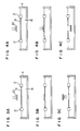
- Figs. 2A and 2B are schematic views of one example of apparatus for producing a polarizer, orientation-controlling film, liquid crystal layer, electrode, semiconductor substrate, etc. used in the liquid crystal display device of the present invention.
- Fig. 2A is a plan view of the apparatus, and Fig. 2B is a side sectional view thereof.
- 1 is a trough
- 2 and 3 are compression barriers
- 4 and 5 are the opposing movement directions of each compression barrier (direction of compression)
- 6 is a water surface on which the film-forming molecules are spread
- 7 is a clean water subphase
- 8 is a water phase.
- the barriers 2 and 3 are moved to the left and right ends, respectively, of the trough to enlarge the area of the water surface 6.
- the film-forming molecules are spread on the water surface 6 in the form of monomolecular film.
- the barriers 2 and 3 are slowly moved toward the right and left, respectively, to compress the spread film on the water surface 6. The movement of the barriers is stopped at the point of time when the surface pressure of the spread film reaches a definite value.
- the film-forming molecules are uniformly oriented, in this condition, in a particular direction in the surface of the film.
- Figs. 2A and 2B show a form of bidirectional compression of the spread film on the gas/liquid interface, but the same result can be also obtained with a unidirectional compression manner frequently seen in the common LB film-forming apparatus.
- the oriented film formed at the gas/liquid interface by the above procedure can be transferred, without being disturbed in the orientational order and orderliness, to a substrate by the lifting method shown in Figs. 3A to 3C or the dipping method shown in Fig. 4A to 4C.
- Figs. 3A to 3C and Figs. 4A to 4C 9 is an oriented film formed on the water surface, 10 is a substrate, and other symbols are the same as those in Figs. 2A and 2B.
- the lifting method Figs. 3A to 3C
- the substrate held nearly horizontally is slowly moved down, and as soon as its surface is brought into contact with the film on the water surface, it is slowly moved up in turn. At that time, the film on the water surface is transferred to the substrate.
- the substrate as held nearly horizontally is slowly moved down and further submerged after brought into contact with the film on the water surface. At that time, the film on the water surface is transferred to the substrate.
- the oriented film formed on the water surface can be deposited in any number of layers on the substrate.
- a first embodiment of the present invention is an organic thin film obtained by spreading an organic substance comprising a polymer on a liquid surface and compressing the spread substance unidirectionally or in two directions facing each other, in which organic thin film the principal chain of the polymer in the surface of the film has been oriented perpendicular to the direction of compression.
- the above-mentioned polymer preferably comprises the polymer in which either or both of the principal chain and side chain contain at least one member selected from the group consisting of the
- the above-mentioned polymer preferably comprises a polydiacetylene derivative represented by the formula (0), wherein R1 and R2 represent independently a side-chain substituent.
- each of the side-chain substituents R1 and R2 preferably has the structure represented by the formula: wherein h is 2 to 18, k is 0 or 1, l is 1 to 18, m is 0 or 1 and n is 0 to 18, all being an integer.
- the above polymer preferably comprises at least one member selected from the group consisting of the polymers represented by the following formulae (1) to (8): wherein R1, R2, R3 and R4 are independently a side-chain substituent.
- (1) is a polypyrrole derivative
- (2) is a polythienylene derivative
- (3) is a poly-p-phenylene derivative and its precursor polymer
- (4) is a poly-p-phenylen vinylene derivative and its precursor polymer
- (5) is a polythienylene vinylene derivative and its precursor polymer
- (6) is a polysilane derivative
- (7) is a polygermane derivative
- (8) is a derivative of a polyacetylene precursor.
- the organic thin film comprising the above polymer it is preferred for the organic thin film comprising the above polymer to keep electrically active conductivity or semiconductivity by itself or by doping.
- At least one of the side-chain substituents, R1, R2, R3 and R4, of the above polymers is preferably either an alkyl group having six or more carbon atoms or an alkyl group containing at least one member selected from the group consisting of a hydroxyl group, amino group, phosphoric acid group, ether group, ester group, peptide group and urethane group.
- the above polymer may be a mixture or copolymer of the above polydiacetylene derivative with one or more members selected from the group consisting of the foregoing polypyrrole derivative (1), polythienylene derivative (2), poly-p-phenylene derivative and its precursor polymer (3), poly-p-phenylene vinylene derivative and its precursor polymer (4), polythienylene vinylene derivative and its precursor polymer (5), polysilane derivative (6), polygermane derivative (7), and the derivative of a polyacetylene precursor (8).
- a second embodiment of the present invention is an organic thin film comprising a plural number of layers of the thin film in which an organic substance is oriented in a particular direction in the surface of the film and which is obtained by spreading the organic substance on a liquid surface and compressing the spread substance unidirectionally or in two directions facing each other, each layer comprising at least two kinds of organic substances or constituent organic substances being different between adjacent layers.
- the above organic substance may comprise a mixture of either one of the above polymers and an organic compound or a dyestuff.
- the above organic compound may have at least one of an electron-donating and electron-attractive structures, whereby the organic thin film keeps electrically active conductivity or semiconductivity.
- the above organic compound may be a porphyrin derivative or a phthalocyanine derivative, whereby the organic thin film keeps electrically active conductivity or semiconductivity, or photoelectric conversion characteristics.
- the above organic compound may be a material having second-order or third-order non-linear optical characteristics.
- the above material having the non-linear optical characteristics may be at least one member selected from the group consisting of an acetylene derivative represented by the formula (I): an ethylene derivative represented by the formula (II): a diazobenzene derivative represented by the formula (III): wherein D is an electron-donating substituent, A is an electron-attractive substituent, and n is 1 or 2.
- the electron-donating substituent D of the above acetylene, ethylene and diazobenzene derivatives has one or more of a hydroxyl, amino, methyl or methoxy group.
- the electron-attractive substituent A of the above acetylene, ethylene and diazobenzene derivatives has one or more of a cyano, carboxyl, nitro, phosphoric acid or sulfonyl group.
- the above organic compound may be a diacetylene derivative.
- the diacetylene derivative By irradiating the organic thin film comprising the above diacetylene derivative with ultraviolet ray, ⁇ ray or electron beam or heat-treating the organic thin film, the diacetylene derivative can be polymerized into polydiacetylene.
- the organic thin film is in contact with a thin film comprising other organic molecules (underlying thin film)
- the orientation direction of the principal chain of polydiacetylene agrees with the molecular arrangement of the underlying thin film.
- a third embodiment of the present invention is a method for producing an organic thin film (hereinafter referred also to as oriented organic thin film-manufacturing method) comprising the steps of spreading an organic substance on a liquid surface to form a thin film at the gas/liquid interface; compressing the resulting thin film unidirectionally or in two directions facing each other to orient the organic substance in a particular direction in the surface of the film at the interface; and then transferring the oriented thin film to a solid substrate by the lifting method or dipping method.
- oriented organic thin film-manufacturing method comprising the steps of spreading an organic substance on a liquid surface to form a thin film at the gas/liquid interface; compressing the resulting thin film unidirectionally or in two directions facing each other to orient the organic substance in a particular direction in the surface of the film at the interface; and then transferring the oriented thin film to a solid substrate by the lifting method or dipping method.
- the in-plane orientation direction of the film In transferring the oriented organic thin film to the solid substrate, it is preferred to control the in-plane orientation direction of the film while monitoring the in-plane orientation direction and the degree of completeness thereof by measuring reflection spectrum or absorption spectrum using linearly polarized light during the formation of the film on the liquid surface.
- a multi-layer structure may be formed, in which the orientation direction may be regulated for every layer.
- An organic substance which is the same as or different from the above organic substance may further be deposited on the organic thin film formed by the above manufacturing method to orient that organic substance in a particular direction.
- the organic substance is deposited by at least one of a vacuum evaporation method, molecular beam epitaxy method, cluster ion beam method, ion beam evaporation method, ion plating method, photo CVD method and plasma CVD method. Further, the deposition of the organic substance may be carried out by at least one of a dipping method, spraying method, spin-coating method, casting method and electrodeposition method, using a solution of the organic substance in an organic or inorganic solvent.
- the deposited organic thin film After the deposition of the organic substance, it is more preferred to heat the deposited organic thin film at a temperature lower than the melting point of the substance.
- butoxycarbonylmethylurethane series polydiacetylene, p-3BCMU represented by the formula (a) in Fig. 5, which is a one-dimensional chain polymer having a good crystallization property and soluble in organic solvents, it can be turned into a thin film which has uniformly been oriented so that the direction of the principal chain is perpendicular to the direction of compression.
- This thin film is an ultra thin film of about 20 ⁇ to about 40 ⁇ in thickness having a large area of about several tens cm2 and a uniform molecular orientation.
- the foregoing oriented organic thin film-manufacturing method may be thought to be widely applicable to the whole polymers having a particular functional group at the principal chain or side chain and being soluble in organic solvents.
- Such polymers having a particular functional group at the principal chain or side chain and being soluble in organic solvents include various polymeric materials expected as electroconducting or semiconducting electronic materials and non-linear optical materials.
- the foregoing polymers such as (0) polydiacetylene derivatives, (1) polypyrrole derivatives, (2) polythienylene derivatives, (3) poly-p-phenylene derivatives and their precursor polymers, (4) poly-p-phenylene vinylene derivatives and their precursor polymers, (5) polythienylene vinylene derivatives and their precursor polymers, (6) polysilane derivatives, (7) polygermane derivatives, and (8) derivatives of polyacetylene precursor polymers.
- the above particular functional group includes an alkyl group having six or more carbon atoms and an alkyl group containing at least one member selected from the group consisting of a hydroxyl group, amino group, phosphoric acid group, ether group, ester group, peptide group and urethane group.
- the above oriented organic thin film-manufacturing method can be applied not only to the above polymers, but also to other polymers and low molecular weight compounds having structural anisotropy which cannot form good oriented thin films by themselves.
- good oriented organic thin films can be formed by mixing the above one-dimensional chain polymers which act as an orientation supporter and the above other polymers or low molecular weight compounds having a structural anisotropy.
- the low molecular weight compound having a structural anisotropy there are mentioned dyes represented by cyanine dyes, merocyanine dyes, etc.; porphyrin derivatives and phthalocyanine derivatives having a photoelectric conversion function; polycyclic aromatic compounds such as perylene, etc.; charge transfer complexes represented by tetracyanoquinodimethane ⁇ tetrathiofluvalene (TCNQ ⁇ TTF); and ⁇ -electron conjugated molecules having second-order or third-order non-linear optical characteristics represented by the foregoing formulae (I) to (III).
- dyes represented by cyanine dyes, merocyanine dyes, etc. porphyrin derivatives and phthalocyanine derivatives having a photoelectric conversion function
- polycyclic aromatic compounds such as perylene, etc.
- orientational order and crystallinity of the above oriented organic thin film can be further improved by heating the thin film or giving a temperature gradient to the thin film during or after compression operation at a gas/liquid interface.
- the ultra-thin oriented thin film produced at a gas/liquid interface by the above method can be transferred to a solid substrate by the lifting method or dipping method, preferably horizontal lifting method.
- Multi-layer thin films can also be formed by repeating this transferring operation many times.
- the substrate used those which are commonly used for thin film formation such as substrates made of glass, ceramics, plastics, metal, semiconductor, etc. may be used. Further, a porous membrane filter marketed from Millipore Ltd. under the trade name of "Millipore Film” and perforated films such as meshes for electron microscopic observation also can be used. Further, adhesiveness between the substrate and oriented organic thin film can also be enhanced by applying a hydrophobic or hydrophilic treatment to the surface of the above substrates.
- a multi-layer thin film is produced by the above method, it is also possible to deposit the oriented thin film formed at a gas/liquid interface, optionally regulating its orientation direction on the substrate for every layer.
- the principal chain of the chain-shaped polymer orients in the direction perpendicular to the compression direction at a gas/liquid interface. Consequently, if the deposition operation is carried out with the substrate turned to a desired direction, it is possible to produce a multi-layer oriented organic thin film in which the principal chain turns to a desired direction at a desired position on the substrate.
- the orientation direction of the oriented organic thin film at a gas/liquid interface by measuring polarization absorption and reflection spectra with a linear polarized light, the orientation of molecules can be more strictly confirmed. This method is therefore useful to control the orientation of mixtures containing a low molecular weight compound.
- Such the multi-layer oriented organic thin film in itself can be utilized as a color polarizing plate, and the light transmittance of the polarizing plate can optionally be controlled by properly adjusting the number of the deposited layers.
- an oriented organic thin films mixed with the above dye(s) can be used as a monochromatic polarizing filter by selecting a dye color having a suitable absorption wavelength.
- said conventional thin film-manufacturing techniques include dry-type thin film-manufacturing methods (e.g. vacuum evaporation method, molecular beam epitaxy method, cluster ion beam method, ion beam evaporation method, ion plating method, photo CVD method, plasma CVD method), and wet-type thin film-manufacturing methods (e.g.
- the reason for this is as follows: Since the epitaxial growth depends largely upon the matching of crystal lattice between the underlying and overlying layers, to use the crystal surface of an organic substance as the underlying layer is considered to more improve the matching of crystal lattice with the overlying organic substance than to use the inorganic crystal as the underlying layer as in the conventional method. It is desirable that the organic substance used as the underlying layer is the same kind as the overlying organic substance, but the both may be different from each other. Consequently, by using the oriented organic thin film as the ground substrate as in the present invention, it is possible to greatly improve the matching of crystal lattice with the overlying organic substance.
- the polydiacetylene compounds shown in Fig. 5 are good examples of the compound the crystal growth of which depends largely upon the matching and epitaxial property of lattice, because solid-phase polymerization of a diacetylene monomer into polydiacetylene is a topochemical polymerization strictly controlled by the steric configuration of monomer crystal lattice.
- an oriented monomer thin film can be formed on the thermally stable oriented polymer thin film, and further other oriented polymer thin films can be obtained by subjecting the monomer thin film to polymerization.
- the oriented organic thin film-manufacturing method of the present invention is useful to form the oriented thin films of porphyrin derivatives and phthalocyanine derivatives expected as photoelectric conversion materials as well as those of the low-molecular-weight diacetylene derivatives expected for second-order and third-order non-linear effects.
- the formation of the epitaxial film of organic molecules on the oriented organic thin film also requires proper control of the inner energy of the molecules before deposition to the substrate, substrate temperature, etc. in order to promote a good epitaxial growth.
- the epitaxial film is not obtained when methods such as the vacuum evaporation method, molecular beam epitaxy method, etc. are used. In such case, the formation of good oriented thin films becomes possible by heat-treating the thin film at a temperature lower than the melting point of the constituent molecule.
- a fourth embodiment of the present invention is a thin and/or flexible liquid crystal display device produced by the LB method as need arises in which part or all of the constituents are composed of organic substances.
- a fifth embodiment of the present invention is a liquid crystal display device with an orientation-controlling film which is superior in the uniformity of film thickness, can easily be formed in a large area and requires no rubbing treatment, heat treatment nor chemicals treatment.
- LB method for forming an organic thin film by successively transferring a monomolecular film spread at a gas/liquid interface to a solid substrate, formation of at least one of (i) a transparent electrode or semiconductor substrate, (ii) a polarizer (analyzer), (iii) an orientation-controlling film and (iv) a liquid crystal layer is easily attained as shown below.
- the transparent electrode or semiconductor substrate is readily composed, by the LB method, of a monomolecular film comprising an electro-conducting polymer such as polypyrrole, polythienylene or a charge transfer complex such as TTF ⁇ TCNQ, pyridium TCNQ complex.
- a monomolecular film comprising an electro-conducting polymer such as polypyrrole, polythienylene or a charge transfer complex such as TTF ⁇ TCNQ, pyridium TCNQ complex.
- the ultra-thin film can also be obtained in the form of a semiconducting organic thin film, and therefore it can be used as a driving device such as thin film transistor (TFT) and metal insulator metal (MIM) by applying fine patterns to it by lithography techniques.
- TFT thin film transistor
- MIM metal insulator metal
- This oriented organic thin film has absorption at 630 to 430 nm, showing a dichroic ratio of 30. It can be used as a polarizer and an analyzer.
- the oriented organic thin film produced by the above organic thin film-manufacturing method can also be used as an orientation-controlling film for liquid crystal display devices.
- This oriented organic thin film itself can also be used as the orientation-controlling film of a liquid crystal without the rubbing treatment.
- the orientation-controlling film can be formed directly on the substrate having an electrode. Further, it is also possible to form the orientation-controlling film on the electrode with an underlying or overlying inorganic insulating film comprising SiO2, Al2O3 or TiO2. Further, adhesiveness between the substrate and orientation-controlling film can be improved by previously applying hydrophobic treatment to the substrate surface with a silane coupling agent such as hexamethyldisilazane.
- the principal chain of the polymer (a film-forming molecule) in the oriented organic thin film formed at a gas/liquid interface as described above, is usually oriented in the direction perpendicular to the compression direction and uniformly over the whole surface. Consequently, if the deposition operation is carried out with the substrate turned to a desired direction, it is possible to produce an orientation-controlling film on the substrate in which the principal chain turns to the desired orientation direction.
- the polymer, a film-forming substance, used in the present invention includes polymers represented by the formulae (0) to (14): wherein substituents R1, R2, R3 and R4 independently represent a structure represented by the formula: wherein h is 2 to 18, k is 0 or 1, l is 1 to 18, m is 0 or 1 and p is 0 to 18.
- the polymers or compounds used in the present invention are not limited to those represented by the above formulae (0) to (14), but may be any of those which are soluble in solvents, particularly organic solvents and can be spread in the form of a thin film at a gas/liquid interface, and can be uniformly oriented in a particular direction in the surface of the thin film when the thin film is compressed unidirectionally or in two directions facing each other.
- a compound unsuitable for thin film formation at a gas/liquid interface can be used as a film-forming substance for the orientation-controlling film if the above oriented organic thin film is utilized as a ground film.
- said compound is deposited as an overlying layer on the oriented organic thin film, which is a ground film, by means such as a vacuum evaporation method, molecular beam epitaxy method, dipping method, spraying method, spinner method, casting method, etc.
- the in-plane orientational order of the ground film can be given to the overlying layer.
- the oriented film comprising the ground film and overlying layer thus obtained also showed an orientation action on the liquid crystal molecule.
- the orientation-controlling film can also be formed on a polymer thin film previously formed to the substrate. That is, the polymer thin film is previously formed as the ground film on the substrate by means such as a dipping method, spraying method, spinner method, casting method, etc., and then the orientation-controlling film according to the present invention is deposited thereon.
- the polymer thin film used as the ground film need not be oriented in the surface of the film. The rubbing treatment of the ground film also is not necessary.
- the thickness of the liquid crystal layer is kept constant by inserting a spacer, and therefore when the liquid crystal cell is bent, the spacer slips off the place to disturb the orientation of the sealed liquid crystal. Disclination is, therefore, sometimes induced.
- a liquid crystal layer free from such a problem can be produced by sealing a liquid crystal in a polymer film having a constant thickness and pores of an area of several tens ⁇ m2.
- the liquid crystal layer can also be produced by a method of impregnating a perforated net-like film such as a porous membrane filter marketed from Millipore Ltd. under the trade name of Millipore Filter with a liquid crystal, and a method of applying a photoresist technique to a transparent polymer film to form a fine and uneven matrix pattern of about several tens ⁇ m and then sealing the liquid crystal into this film.
- a perforated net-like film such as a porous membrane filter marketed from Millipore Ltd. under the trade name of Millipore Filter
- a method of applying a photoresist technique to a transparent polymer film to form a fine and uneven matrix pattern of about several tens ⁇ m and then sealing the liquid crystal into this film.
- the liquid crystal used in the liquid crystal display device of the present invention can be selected from a fairly wide range, if it shows a nematic phase or smectic phase in a working temperature range.
- the liquid crystal includes compounds shown in Table 1, their derivatives and mixtures thereof.
- R′ represents alkyl or alkoxyl
- X represents cyano, nitro or halogen
- liquid crystal display devices of the present invention when the liquid crystal is a nematic one, its molecules enclosed between two substrates can take any of the following alignment forms:
- ferroelectric liquid crystals as shown below also can be used as the liquid crystal:
- the orientation-controlling film according to the present invention is characterized in that the polymer constituting the film is uniformly oriented in a particular direction in the film surface. Such the uniform orientation of the molecule in the surface of the film may be presumed to be one of factors causing the orientation action on liquid crystal molecules.
- This thin and flexible liquid crystal display device can be produced in not only transparent forms, but also reflective forms. Also, this device can be stuck on windows, fences, partitions between two rooms, doors, blinds, front panel of automobile displays, sun-roofs, illuminators, displays, show windows, mirrors, toys, etc.
- the orientation-controlling film in a manner described in (iii), it can be incorporated into the liquid crystal display device without the rubbing treatment, heat treatment and chemicals treatment. Also, such the orientation-controlling film is superior in the uniformity of film thickness and also can easily be produced in a large area.
- p-3BCMU polydiacetylene derivative
- the side-chain substituent is an alkyl chain containing a urethane and ester moieties and which is represented by the structural formula shown in Fig. 5(a).
- R1 and R2 in Fig. 5 are a side-chain substituent of the polydiacetylene derivative.
- This p-3BCMU is a polymer having an average chain length of about 1 ⁇ m and being soluble in chloroform.
- a 0.5 g/l chloroform solution of this polymer was prepared, and several drops of the solution were spread on pure water contained in a trough of the LB film-manufacturing apparatus. After chloroform completely volatilized, the spread film was compressed in two directions facing each other at a compression rate of 100 cm2/min to hold the monomolecular film at a surface pressure of 20 mN/m.
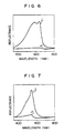
- the in-plane orientational order of the p-3BCMU monomolecular film thus produced on the water surface was evaluated by measuring a polarized reflection spectrum.
- the measurement with polarized light was carried out by employing linearly polarized light vertically incident on the monolayer on the water surface.
- the intensity of the polarization reflection spectrum was maximum and minimum when the direction of polarization was perpendicular ( ⁇ ) to and parallel ( ⁇ ) to the compression direction, respectively.
- Symbols ⁇ and ⁇ in Fig. 6 show that the electric field vector of the linearly polarized light is perpendicular to and parallel to the compression direction, respectively.
- the oriented organic thin film of p-3BCMU produced at the air/water interface could easily be transferred to glass, quartz, ITO and silicon substrates, previously subjected to hydrophobic treatment with hexamethyldisilazane, which is one of the silane coupling agents, by the horizontal lifting method or horizontal immersing method.
- the p-3BCMU oriented organic thin film formed on any of these substrates was a good-quality film of about 27 ⁇ in thickness retaining a high orientational order of p-3BCMU.
- p-4BCMU polydiacetylene derivative
- p-4BCMU polydiacetylene derivative
- p-3BCMU polydiacetylene derivative
- the structural formula of this compound is shown in Fig. 5(b).
- a 0.5 g/l chloroform solution of this polymer was prepared, and several drops of the solution were spread on pure water contained in a spreading vessel of the LB film-manufacturing apparatus. After chloroform completely volatilized, the spread film was compressed in two directions facing each other at a compression rate of 100 cm2/min to hold the monomolecular film at a surface pressure of 20 mN/m.
- the in-plane orientational order of the p-4BCMU monomolecular film thus produced on the water surface was evaluated by measuring a polarized reflection spectrum in the same manner as in Example 1.
- the intensity of the polarization reflection spectrum was maximum and minimum when the direction of polarization was perpendicular ( ⁇ ) to and parallel ( ⁇ ) to the compression direction, respectively, in the similar manner to the case of p-3BCMU in Example 1.
- Symbols ⁇ and ⁇ in Fig. 7 show that the electric field vector of the linearly polarized light is perpendicular to and parallel to the compression direction, respectively.
- the oriented organic thin film of p-4BCMU produced at the air/water interface could easily be transferred to glass, quartz, ITO and silicon substrates, previously subjected to hydrophobic treatment with hexamethyldisilazane, by the horizontal lifting method or horizontal immersing method.
- the p-4BCMU oriented organic thin film formed on any of these substrates was a good-quality film of about 31 ⁇ in thickness retaining a high orientational order.
- the film-forming substance As the film-forming substance was used a mixture of poly(3-hexadecylthienylene) (hereinafter referred to as PHDT) having as the side-chain substituent an alkyl chain represented by the structural formula of Fig. 8A and a polydiacetylene derivative (p-3BCMU) used in Example 1. Both these polymers were a polymer having an average chain length of about 1 ⁇ m and being soluble in chloroform. A chloroform solution of the 1:1 mixture of these polymers was prepared, and several drops of the solution were spread on pure water contained in the trough of the LB film-manufacturing apparatus. After chloroform completely volatilized, the spread film was compressed in two directions facing each other at a compression rate of 100 cm2/min to hold the monomolecular film at a surface pressure of 20 mN/m.
- PHDT poly(3-hexadecylthienylene)
- p-3BCMU polyd
- the in-plane orientational order of the mixed monomolecular film thus produced on the water surface was evaluated by measuring a polarized reflection spectrum in the same manner as in Example 1.
- the intensity of the polarization reflection spectrum was maximum and minimum when the direction of polarization was perpendicular ( ⁇ ) to and parallel ( ⁇ ) to the compression direction, respectively. From this result, it became clear that both the principal chains of these one-dimensional chain polymers have been oriented at a right angle to the compression direction. Also, it became clear that, since this polarization characteristics do not show in-plane position dependency, the principal chains have been oriented in the same direction and uniformly over the whole monomolecular film of about 50 cm2 in area.
- Ten layers of the oriented organic thin film of the mixture thus produced on the air/water interface were deposited one upon another on a quartz substrate, previously subjected to hydrophobic treatment, by the horizontal lifting method so that the orientation directions of the principal chains were the same. Further, the polarized absorption spectrum of the oriented organic thin film of the mixture deposited on the substrate was measured to find that the dichroic ratio at the absorption peak of about 620 nm resulting from the ⁇ - ⁇ * exciton of the one-dimension principal chain of p-3BCMU was about 6, and that the dichroic ratio at the absorption peak of about 490 nm resulting from the ⁇ - ⁇ * transition of the one-dimensional principal chain of PHDT was about 3.
- the film-forming substance As the film-forming substance was used a mixture of the precursor polymer of a polyphenylene vinylene derivative represented by the structural formula of Fig. 8B and the polydiacetylene derivative (p-3BCMU) used in Example 1. Both these polymers were a polymer having an average chain length of about 1 ⁇ m and being soluble in chloroform. A chloroform solution of the 1:1 mixture of these polymers was prepared, and several drops of the solution were spread on pure water contained in the trough of the LB film-manufacturing apparatus. After chloroform completely volatilized, the spread film was compressed in two directions facing each other at a compression rate of 100 cm2/min to hold the monomolecular film at a surface pressure of 20 mN/m.
- the in-plane orientational order of the mixed monomolecular film thus produced on the water surface was evaluated by measuring a polarized reflection spectrum in the same manner as in Example 1.
- the intensity of the polarization reflection spectrum was maximum and minimum when the direction of polarization was perpendicular ( ⁇ ) to and parallel ( ⁇ ) to the compression direction, respectively. From this result, it became clear that both the principal chains of these one-dimensional chain-shaped polymers have been oriented perpendicularly to the compression direction. Also, it became clear that, since this polarization characteristics do not show in-plane position dependency, the principal chains have been oriented in the same direction and uniformly over the whole monomolecular film of about 50 cm2 in area.
- the polarized absorption spectrum of this heat-treated oriented organic thin film was measured to find that the dichroic ratio at the absorption peak of about 620 nm resulting from the ⁇ - ⁇ * exciton of the one-dimensional principal chain of p-3BCMU was about 6, and that the dichroic ratio at the absorption peak of about 480 nm resulting from the electron transition of the one-dimensional principal chain of the polyphenylene vinylene derivative was about 4.
- PDHS polydihexylsilane
- p-3BCMU polydiacetylene derivative
- the in-plane orientational order of the mixed monomolecular film thus produced on the water surface was evaluated by measuring a polarized reflection spectrum in the same manner as in Example 1.
- the intensity of the polarization reflection spectrum was maximum and minimum when the direction of polarization was perpendicular ( ⁇ ) to and parallel ( ⁇ ) to the compression direction, respectively. From this result, it became clear that both the principal chains of these one-dimensional chain polymers have been oriented perpendicularly to the compression direction. Also, it became clear that, since this polarization characteristics do not show in-plane position dependency, the principal chains have been oriented in the same direction and uniformly over the whole monomolecular film of about 50 cm2 in area.
- the oriented organic thin film of the mixture produced at the air/water interface could easily be transferred to glass, quartz and silicon substrates, previously subjected to hydrophobic treatment with hexamethyldisilazane, by the horizontal lifting method. Further, the polarized absorption spectrum of the oriented organic thin film of this mixture deposited on the substrates was measured to find that the dichroic ratio at the peak of about 620 nm resulting from the ⁇ - ⁇ * exciton of the one-dimensional principal chain of p-3BCMU was about 8, and that the dichroic ratio at the peak of about 370 nm resulting from the electron transition of the one-dimensional principal chain of PDHS was about 4.
- the film-forming substance As the film-forming substance was used a mixture of a merocyanine dye having an alkyl chain represented by the structural formula of Fig. 8E and the polydiacetylene derivative (p-4BCMU) used in Example 2.
- a chloroform solution containing one dye molecule per one monomer unit of the derivative was prepared, and several drops of the solution were spread on an aqueous cadmium chloride solution contained in the trough of the LB film-manuafcturing apparatus. After chloroform completely volatilized, the spread film was compressed in two directions facing each other at a compression rate of 100 cm2/min to hold the monomolecular film at a surface pressure of 25 mN/m.
- the in-plane orientational order of the mixed monomolecular film thus produced on the water surface was evaluated by measuring a polarization reflection spectrum in the same manner as in Example 1.
- the intensity of the polarized reflection spectrum was maximum and minimum when the direction of polarization was perpendicular ( ⁇ ) to and parallel ( ⁇ ) to the compression direction, respectively.
- the dichroic ratio at the peak of about 540 nm resulting from the ⁇ - ⁇ * exciton of the one-dimensional principal chain of p-4BCMU was about 8
- the dichroic ratio at the peak of about 600 nm resulting from the electron transition of the J-aggregate of the merocyanine dye was about 4.
- the oriented organic thin film of the mixture produced at the air/water interface could easily be transferred to a quartz substrate by the horizontal lifting method.
- the film showed no change in film quality even after transferred to the substrate.
- Example 2 On the oriented organic thin film of p-3BCMU produced on a glass substrate in the same manner as in Example 1, was deposited a diacetylene derivative shown in Fig. 9A by the vacuum evaporation method. Thus, a diacetylene monomer thin film of about 1 ⁇ m in thickness was obtained. Thereafter, the monomer was polymerized by ultraviolet irradiation to obtain a polymer thin film having an area of about 40 cm2.
- Fig. 9B shows the polarized absorption spectrum measured with a linearly polarized light of the above polymer thin film.
- the intensity of the absorption peak resulting from the polymer principal chain was maximum and minimum when the direction of polarization was parallel ( ⁇ ) to and perpendicular ( ⁇ ) to the orientation direction, respectively, of the principal chain of p-3BCMU constituting the monomolecular film used as a ground film.
- Symbols ⁇ and ⁇ in Fig. 9B shows that the electric field vector of the linearly polarized light is perpendicular to and parallel with the orientation direction, respectively, of the principal chain of the polydiacetylene constituting the ground film.
- the dichroic ratio at the peak of about 620 nm resulting from the ⁇ - ⁇ * exciton of the one-dimensional principal chain of the polydiacetylene (p-3BCMU) was about 6. Further, it was found that, since this polarization characteristics do not show in-plane position dependency, the principal chain of p-3BCMU has been oriented in the same direction and uniformly over the whole thin film. Consequently, it was found that the overlying polydiacetylene thin film produced as above by the vacuum evaporation method was a good epitaxial film controlled by the orientation direction of the underlying p-3BCMU layer.
- a diacetylene derivative hereinafter referred to as DCH
- Fig. 10A a diacetylene derivative shown in Fig. 10A by the vacuum evaporation method.
- DCH diacetylene derivative
- p-DCH polydiacetylene
- Fig. 10B shows the polarization absorption spectrum measured with a linerly polarized light of the above polydiacetylene thin film.
- the intensity of the absorption peak resulting from the polymer principal chain was maximum and minimum when the direction of polarization was parallel ( ⁇ ) to and perpendicular ( ⁇ ) to the orientation direction, respectively, of the principal chain of p-3BCMU constituting the monomolecular film used as a ground film.
- Symbols ⁇ and ⁇ in Fig. 10B shows that the electric field vector of the linearly polarized light is perpendicular to and parallel to the orientation direction, respectively, of the principal chain of the polydiacetylene constituting the ground film.
- the dichroic ratio at the peak of about 650 nm resulting from the ⁇ - ⁇ * exciton of the one-dimensional principal chain of the polydiacetylene (p-DCH) was about 5. Further, it was found that, since this polarization characteristics do not show in-plane position dependency, the principal chain of p-DCH has been oriented in the same direction and uniformly over the whole thin film. Consequently, it was found that the overlying polydiacetylene (p-DCH) thin film produced as above by the vacuum evaporation method was a good epitaxial film controlled by the orientation direction of the underlying p-3BCMU layer.
- a phthalocyanine thin film having a thickness of about 0.5 ⁇ m and a film area of about 40 cm2 was obtained.
- Fig. 11b shows the polarized absorption spectrum measured with a linearly polarized light of the above phthalocyanine thin film obtained.
- the intensity of the absorption peak of the phthalocyanine was maximum and minimum when the direction of polarization was perpendicular ( ⁇ ) to and parallel ( ⁇ ) to the orientation direction, respectively, of the principal chain of p-3BCMU constituting the monomolecular film used as a ground film.
- Symbols ⁇ and ⁇ in Fig. 11b shows that the field vector of linearly polarized light is perpendicular to and parallel to the orientation direction, respectively, of the principal chain of the polydiacetylene constituting the ground film.
- the dichroic ratio at the peak of about 650 nm resulting from the ⁇ - ⁇ * excitation in the molecular surface of phthalocyanine was about 9. Further, it was found that, since this polarization characteristics do not show in-plane position dependency, this phthalocyanine thin film was a good epitaxial film in which the one-dimensional molecular column of phthalocyanine has been oriented in the same direction and uniformly over the whole thin film. Thereafter, the above thin film was heat-treated at 100°C for 10 hours, and the polarization characteristics were again evaluated. As a result, it was found that the dichroic ratio rose to about 12, and so the epitaxial property was promoted by the heat treatment.
- the oriented film of the polydiacetylene (p-3BCMU) having a thickness of 1 ⁇ m and a dichroic ratio of about 6 produced in Example 7 was evaluated for the third-order non-linear optical effect.
- ⁇ (3) was evaluated by irradiating the above thin film with a laser beam of 1.9 ⁇ m in wavelength and measuring the intensity of a third harmonic wave (0.63 ⁇ m) by the Maker fringe method.
- the similar result was obtained with the oriented thin film of the polydiacetylene (p-DCH) produced in Example 8.
- Two pieces of a transparent polyethylene film of 500 ⁇ m in thickness and 5 x 5 cm in area were used as an upper and lower substrates of a liquid crystal cell.
- a monomolecular film consisting of a pyrrole derivative having a alkyl chain (Fig. 12A) was prepared on the liquid surface of a 1 x 10 ⁇ 3 M aqueous ferric chloride solution.
- Two layers of this monomolecular film were deposited in the form of the Y-type on one side of each polyethylene film and treated with the vapor of ferric chloride to obtain two pieces of a transparent electrode film having an electric conductivity of 10 ⁇ 2 S/cm.
- a 0.5 g/l chloroform solution of a polydiacetylene derivative (p-3BCMU, Fig. 12B) was prepared, and several drops of the solution were spread at an air/water interface.
- the spread film was compressed in two directions facing each other to produce a monomolecular film in which the principal chain of the polydiacetylene has been uniformly oriented perpendicularly to the compression direction under a surface pressure of about 20 mN/m.
- Ten layers of this monomolecular film were deposited one upon another on the pyrrole derivative side of each transparent electrode film by the horizontal lifting method so that all the films took the same in plane orientation direction.
- an orientation-controlling film showing absorption at 630 to 430 nm and having a transmittance of about 50% and a dichroic ratio of about 15 was produced on each transparent electrode film.
- This orientation-controlling film can be used without the rubbing treatment and also has a function as a polarizing film.
- PMMA Polymethyl methacrylate
- Fig. 12C a mixed nematic liquid crystal
- ZLI-1132 a mixed nematic liquid crystal
- a weight ratio of 2:1 were dissolved in p-xylene, and this solution was cast to an air/water interface. After 30 minutes, vaporization of p-xylene and solidification of PMMA were confirmed, and the resulting liquid crystal film was transferred, by the horizontal lifting method, onto one of the transparent electrode films with the orientation-controlling film (combining the function of a polarizing film) thereon.
- a liquid crystal cell of a sandwich structure having a total thickness of 2 mm or less was obtained as shown in Fig. 13.
- 1 is a transparent polyethylene film
- 2 is an electrode comprising the pyrrole derivative
- 3 is an orientation-controlling film
- 4 is a liquid crystal layer.
- This liquid crystal cell showed a light transmittance-voltage curve as shown in Fig. 14 in which the light transmittance is high when no electric field is applied and decreases when AC electric field of 30 kHz is applied.
- This liquid crystal cell showed the same light transmittance-voltage characteristics as above even when held at its both ends and bent at a right angle, and also unevenness in the light transmittance was not observed over the whole cell. Consequently, it was confirmed that this liquid crystal cell is a good flexible thin-film liquid crystal display device.
- the monomolecular film of p-3BCMU was formed on the water surface in the same manner as in Example 1. It was found that the oriented monomolecular film of p-3BCMU could be deposited in a large number of layers on a substrate by repeating the procedure shown in Figs. 3A to 3C or Figs. 4A to 4C. The X-ray diffraction of this multi-layer p-3BCMU film was measured to find that the film thickness per one molecular layer of the p-3BCMU film was about 27 ⁇ .
- Ten layers of the oriented monomolecular film (oriented organic thin film) of p-3BCMU formed on the water surface by the above method were deposited one upon another on a glass substrate with an ITO electrode, previously subjected to hydrophobic treatment with hexamethyldisilazane, by the horizontal lifting method so that the principal chains took the same orientation direction.
- another piece of a glass substrate with an ITO electrode on which ten layers of the p-3BCMU monomolecular film were deposited one upon another was prepared. These two substrates were put opposite to each other through a spacer of 8 ⁇ m so that the p-3BCMU film of each substrate turned inward and the orientation directions of the films intersected perpendicularly to each other.
- a cell was obtained.
- a nematic liquid crystal marketed from Merk Co. under the name of ZLI-1132 as a mixture of the following four compounds, was sealed into the cell: Further, one piece of a polarizing plate was stuck on the respective outer sides of two substrates constituting the cell. At that time, the polarization axis of each polarizing plate was regulated so that it agreed with the orientation direction of the p-3BCMU film near the plate.
- the schematic view of the cell in this Example will be shown in Fig. 15. In the drawing, 11 and 19 are a polarizing plate, 12 and 18 are a glass plate, 13 and 17 are an ITO electrode, 14 and 16 are a p-3BCMU film, 15 is a spacer and 20 is a liquid crystal layer.
- the liquid crystal display device thus obtained showed no unevenness of orientation, and thus a uniform liquid crystal orientation proved to have been realized.
- the response characteristics of this device were measured at a frequency of 32 Hz and an applied voltage of 5 V to obtain a result that the rise time was ms and the decay time was 20 ms.
- Fig. 16 is a graph showing the threshold voltage characteristics in terms of a relationship between voltage (V, abscissa) and transmittance (%, ordinate).
- the p-3BCMU oriented thin film formed according to the present invention shows a good orientation action on the liquid crystal molecules.
- Example 12 The same procedure was repeated as in Example 12 except that p-4BCMU was used as the film-forming molecule. It was also found that the oriented monomolecular film of p-4BCMU could be deposited in a large number of layers on a substrate in completely the same manner as in Example 12. The X-ray diffraction of this multi-layer p-4BCMU film was measured to find that the film thickness per one molecular layer of the p-4BCMU film was about 31 ⁇ .
- a liquid crystal display device was produced using p-4BCMU oriented film formed by the above method as the liquid crystal orientation-controlling film. Its constitution and nematic liquid crystal used were completely the same as used in Example 12. The liquid crystal display device thus obtained showed no unevenness of orientation, and thus a uniform liquid crystal orientation proved to have been realized. Also, the electro-optical characteristics of this device were almost the same as those of the device in Example 12.
- the p-4BCMU oriented thin film formed according to the present invention shows a good orientation action on the liquid crystal molecules.
- the monomolecular film of a mixture of PHDT and p-3BCMU was formed on a water surface in the same manner as in Example 3.
- a liquid crystal display device was produced using this film as the orientation-controlling film. Its constitution and nematic liquid crystal used were completely the same as used in Example 12. The liquid crystal display device thus obtained showed no unevenness of orientation, and thus a uniform liquid crystal orientation proved to have been realized. Also, the electro-optical characteristics of this device were almost the same as those of the device in Example 12.
- the mixed oriented film of PHDT and p-3BCMU formed according to the present invention shows a good orientation action on the liquid crystal molecules.
- the monomolecular film of a mixture of PDHS and p-3BCMU was formed in the same manner as in Example 5.
- a liquid crystal display device was produced using this film as the orientation-controlling film. Its constitution and nematic liquid crystal used were completely the same as used in Example 12. The liquid crystal display device thus obtained showed no unevenness of orientation, and thus a uniform liquid crystal orientation proved to have been realized. Also, the electro-optical characteristics of this device were almost the same as those of the device in Example 12.
- the mixed oriented film of PDHS and p-3BCMU formed according to the present invention shows a good orientation action on the liquid crystal molecules.
- Example 12 On the oriented thin film of p-3BCMU produced on a glass substrate in the same manner as in Example 12 was deposited a diacetylene derivative (DCH) represented by the formula, by the vacuum evaporation method. Thus, a diacetylene monomer thin film of about 1500 ⁇ in thickness was obtained. Thereafter, the monomer was polymerized by ultraviolet irradiation to obtain a polymer (p-DCH) thin film.
- DCH diacetylene derivative
- the polarized absorption spectrum of the polymer thin film thus produced was measured to find that the intensity of the absorption peak resulting from the polymer principal chain was maximum and minimum when the polarization direction was parallel to and perpendicular to the orientation direction, respectively, of the principal chain of the p-3BCMU monomolecular film used as a ground film.
- the dichroic ratio at the absorption peak of about 650 nm resulting from the p-DCH principal chain was about 5. It was found that, since this polarization characteristics do not show in-plane position dependency, the principal chain of p-DCH has been oriented in the same direction and uniformly over the whole thin film.
- a liquid crystal display device was produced using as the orientation-controlling film the poly-DCH oriented film produced on the p-3BCMU oriented thin film by the above method. Its constitution and nematic liquid crystal used were completely the same as used in Example 12. The liquid crystal display device thus obtained showed no unevenness of orientation, and thus a uniform liquid crystal orientation proved to have been realized. Also, the electro-optical characteristics of this device were almost the same as those of the device in Example 12.
- the p-DCH oriented thin film formed according to the present invention shows a good orientation action on the liquid crystal molecules.
- This polyamide acid varnish was applied to a glass substrate with an ITO electrode by means of a spinner, and baked at 300°C to obtain a polyimide thin film of about 800 ⁇ in thickness.
- Example 12 On the polyimide thin film prepared by the above method were deposited five layers of the p-3BCMU monomolecular film in the same manner as in Example 12 to form a polyimide/p-3BCMU composite film. A liquid crystal display device was then produced using this composite film as the orientation-controlling film. Its constitution and nematic liquid crystal used were the same as in Example 12 except that the above composite film was used as the orientation-controlling film. A schematic sectional view of this device is shown in Fig. 17. In this drawing, 21 and 24 are a polyimide thin film, 22 and 23 are a p-3BCMU monomolecular film and other numbers are the same as in Fig. 15. The liquid crystal display device thus obtained showed no unevenness of orientation, and thus a uniform liquid crystal orientation proved to have been realized. Also, the electro-optical characteristics of this device were almost the same as those of this device in Example 12.
- the p-3BCMU oriented thin film produced on the polyimide ground film according to the present invention shows a good orientation action on the liquid crystal molecules.
- Example 12 In the same manner as in Example 12, six layers of the oriented monomolecular film of p-3BCMU were deposited on a glass substrate with an ITO electrode so that the direction of the principal chain was the same for all the layers.
- the in-plane orientation direction of the p-3BCMU film on each substrate was determined so that the angle of twist of liquid crystal molecules inserted between the two glass substrates was 220 degrees.
- a spacer of 6 ⁇ m in thickness was inserted between these substrates to obtain a cell.
- a liquid crystal composition consisting of a nematic liquid crystal mixture having the following composition, and about 0.5 wt.% of S-811 (made by Merk Co.) which is an optically active substance was sealed into the cell.
- the oriented thin film produced by the method of the present invention can also be used for the STN device.
- Example 12 In the same manner as in Example 12, three layers of the oriented monomolecular film of p-3BCMU were deposited in three layers on a glass substrate with a stripe-form transparent electrode (electrode width, 200 ⁇ m; distance between electrodes, 50 ⁇ m) so that the direction of the principal chain was the same for all the layers. Another piece of completely the same specimen was prepared. These two substrates were put opposite to each other through a spacer of 4 ⁇ m so that the p-3BCMU film of each substrate turned inward and the orientation directions of the principal chain of the respective p-3BCMU films intersected perpendicularly to each other. Thus, a cell was obtained. Next, a ferroelectric liquid crystal composition consisting of was sealed into the cell.
- a polarizing plate was stuck on the respective outer sides of the two substrates constituting the cell.
- the polarization axis of each polarizing plate was regulated so that it agreed with the orientation direction of the p-3BCMU film near the plate.
- the liquid crystal display device thus obtained showed no unevenness of orientation, and thus a uniform orientational order proved to have been realized.
- the electro-optical characteristics of this device were measured to obtain the results as shown in Fig. 18.
- Fig. 18 shows the memory characteristics of this device in relationships of time vs. applied voltage and time vs. brightness. It can be seen from Fig. 18 that the device of this Example has good memory characteristics.
- the p-3BCMU oriented thin film produced by the method of the present invention shows a good orientation action also on a ferroelectric liquid crystal molecule.
- Example 12 In the same manner as in Example 12, three layers of the oriented monomolecular film of p-3BCMU were deposited respectively on glass substrates with an ITO electrode so that the direction of the principal chain was the same for all the layers.
- the in-plane orientation direction of the p-3BCMU film on each substrate was determined so that liquid crystal molecules inserted between the two glass substrates took a homogeneous orientation.
- a spacer of 10 ⁇ m in thickness was inserted between these substrates to obtain a cell.
- the absorption spectrum of the guest ⁇ host-type device (GH device) thus produced was measured using two kinds of polarized lights which are parallel to and normal to the orientation direction of the liquid crystal molecule, and the dichroic ratio of the above dye was obtained from the absorbances, A ⁇ and A ⁇ , of the dye for the two polarized lights.
- the wavelength at a maximum absorption of the dye was 522 nm and the dichroic ratio at this wavelength was 6.3.
Landscapes
- Physics & Mathematics (AREA)
- Chemical & Material Sciences (AREA)
- Engineering & Computer Science (AREA)
- Crystallography & Structural Chemistry (AREA)
- Nonlinear Science (AREA)
- General Physics & Mathematics (AREA)
- Nanotechnology (AREA)
- Materials Engineering (AREA)
- Mathematical Physics (AREA)
- Optics & Photonics (AREA)
- Condensed Matter Physics & Semiconductors (AREA)
- Organic Chemistry (AREA)
- Spectroscopy & Molecular Physics (AREA)
- Composite Materials (AREA)
- Manufacturing & Machinery (AREA)
- Liquid Crystal (AREA)
Applications Claiming Priority (6)
| Application Number | Priority Date | Filing Date | Title |
|---|---|---|---|
| JP1241990A JPH03105322A (ja) | 1989-09-20 | 1989-09-20 | 液晶表示素子 |
| JP241990/89 | 1989-09-20 | ||
| JP241975/89 | 1989-09-20 | ||
| JP1241975A JPH03105315A (ja) | 1989-09-20 | 1989-09-20 | 液晶表元装置 |
| JP246289/89 | 1989-09-25 | ||
| JP24628989A JPH03109431A (ja) | 1989-09-25 | 1989-09-25 | 有機薄膜およびその作製方法 |
Publications (2)
| Publication Number | Publication Date |
|---|---|
| EP0418833A2 true EP0418833A2 (fr) | 1991-03-27 |
| EP0418833A3 EP0418833A3 (en) | 1993-03-17 |
Family
ID=27332994
Family Applications (1)
| Application Number | Title | Priority Date | Filing Date |
|---|---|---|---|
| EP19900117959 Withdrawn EP0418833A3 (en) | 1989-09-20 | 1990-09-18 | Organic thin film and liquid crystal display devices with the same |
Country Status (2)
| Country | Link |
|---|---|
| US (1) | US5357357A (fr) |
| EP (1) | EP0418833A3 (fr) |
Cited By (4)
| Publication number | Priority date | Publication date | Assignee | Title |
|---|---|---|---|---|
| EP0449047B1 (fr) * | 1990-03-15 | 1999-05-26 | Canon Kabushiki Kaisha | Dispositif à cristal liquide, procédé d'affichage et système d'affichage l'utilisant |
| EP1431266A4 (fr) * | 2001-08-27 | 2005-06-15 | Japan Science & Tech Agency | Polymere sensible a la lumiere, polymere de diacetylene de type compose, cristaux de carboxylates d'ammonium, et leurs procedes de production |
| US11217764B2 (en) | 2001-12-05 | 2022-01-04 | Semiconductor Energy Laboratory Co., Ltd. | Organic semiconductor element |
| CN121801144A (zh) * | 2026-03-12 | 2026-04-07 | 江汉大学 | 外电场诱导聚酰亚胺分子排列提高透明性的方法、系统及聚酰亚胺薄膜 |
Families Citing this family (18)
| Publication number | Priority date | Publication date | Assignee | Title |
|---|---|---|---|---|
| US5892244A (en) * | 1989-01-10 | 1999-04-06 | Mitsubishi Denki Kabushiki Kaisha | Field effect transistor including πconjugate polymer and liquid crystal display including the field effect transistor |
| JPH06347799A (ja) * | 1993-06-04 | 1994-12-22 | Canon Inc | 強誘電性液晶素子 |
| JPH07152024A (ja) * | 1993-05-17 | 1995-06-16 | Sharp Corp | 液晶表示素子 |
| JPH09123513A (ja) * | 1995-11-06 | 1997-05-13 | Fuji Xerox Co Ltd | 導電性高分子薄膜及びその製造方法、導電性高分子薄 膜の駆動方法並びに画像形成方法及び画像形成装置 |
| US6399166B1 (en) * | 1996-04-15 | 2002-06-04 | Optiva, Inc. | Liquid crystal display and method |
| US6346975B2 (en) * | 1998-08-04 | 2002-02-12 | International Business Machines Corporation | Liquid crystal display having alignment layer using ion bombarded amorphous material 100Å thickness or less |
| DE19933843B4 (de) * | 1999-07-20 | 2005-02-17 | Robert Bosch Gmbh | Eine Schicht, die elektrisch leitfähiges, transparentes Material enthält, ein Verfahren zur Herstellung einer solchen Schicht und deren Verwendung |
| US7431968B1 (en) * | 2001-09-04 | 2008-10-07 | The Trustees Of Princeton University | Process and apparatus for organic vapor jet deposition |
| AU2003212458A1 (en) | 2002-02-26 | 2003-09-09 | Board Of Regents, The University Of Texas System | Cyclo(n)pyrroles and methods thereto |
| EP1584114A1 (fr) * | 2003-01-17 | 2005-10-12 | Diode Solutions, Inc. | Afficheur utilisant une matiere organique |
| JP5374673B2 (ja) * | 2006-04-04 | 2013-12-25 | シリコール マテリアルズ インク | 珪素精製方法 |
| US9741901B2 (en) | 2006-11-07 | 2017-08-22 | Cbrite Inc. | Two-terminal electronic devices and their methods of fabrication |
| US8222077B2 (en) * | 2006-11-07 | 2012-07-17 | Cbrite Inc. | Metal-insulator-metal (MIM) devices and their methods of fabrication |
| US7898042B2 (en) | 2006-11-07 | 2011-03-01 | Cbrite Inc. | Two-terminal switching devices and their methods of fabrication |
| JP2008165385A (ja) * | 2006-12-27 | 2008-07-17 | Dainippon Printing Co Ltd | 赤外線反射パターン印刷透明シート |
| JP2008180798A (ja) * | 2007-01-23 | 2008-08-07 | Dainippon Printing Co Ltd | パターン印刷透明シート |
| US11513071B2 (en) * | 2019-10-15 | 2022-11-29 | 2Witech Solutions Llc | Sensing device for detecting analyte containing non-metallic element, and method thereof |
| CN115220267B (zh) * | 2022-08-01 | 2023-07-25 | 南京大学 | 一种液晶注液多孔光滑表面构建方法及其微流控应用 |
Family Cites Families (37)
| Publication number | Priority date | Publication date | Assignee | Title |
|---|---|---|---|---|
| US3966304A (en) * | 1973-08-20 | 1976-06-29 | Asahi Kogaku Kogyo Kabushiki Kaisha | Liquid crystal display device |
| US3941901A (en) * | 1974-02-15 | 1976-03-02 | Hoffmann-La Roche Inc. | Surface alignment method for liquid crystal cells and production of polarizers therefor |
| JPS5510180B2 (fr) * | 1974-12-04 | 1980-03-14 | ||
| JPS5319042A (en) * | 1976-08-05 | 1978-02-21 | Seiko Epson Corp | Liquid crystal display device |
| JPS5376049A (en) * | 1976-12-17 | 1978-07-06 | Hitachi Ltd | Affixing method of polariizing plates of varying characteristics |
| US4241984A (en) * | 1979-06-04 | 1980-12-30 | Timex Corporation | Simplified field effect, twisted nematic liquid crystal display construction |
| IL60116A (en) * | 1979-06-25 | 1984-04-30 | University Patents Inc | Coating process and articles coated thereby |
| JPS5831318A (ja) * | 1981-08-19 | 1983-02-24 | Nec Corp | 液晶表示素子及びその製造法 |
| JPS5891427A (ja) * | 1981-11-27 | 1983-05-31 | Toray Ind Inc | 液晶表示素子 |
| JPS58120220A (ja) * | 1982-01-11 | 1983-07-18 | Nitto Electric Ind Co Ltd | ネガ・ポジ同時表示用偏光板 |
| JPH0769535B2 (ja) * | 1982-09-28 | 1995-07-31 | 日東電工株式会社 | 偏光子 |
| JPS59210416A (ja) * | 1983-05-14 | 1984-11-29 | Sharp Corp | フイルム基板液晶表示素子の製造方法 |
| JPS60216337A (ja) * | 1984-04-12 | 1985-10-29 | Canon Inc | デジタル並列光演算装置 |
| JPS60222824A (ja) * | 1984-04-20 | 1985-11-07 | Matsushita Electric Ind Co Ltd | 液晶表示装置 |
| JPS6159428A (ja) * | 1984-08-31 | 1986-03-26 | Fujitsu Ltd | 液晶表示素子 |
| GB8513770D0 (en) * | 1985-05-31 | 1985-07-03 | Gen Electric Co Plc | Optically non-linear materials |
| JPS61278827A (ja) * | 1985-06-04 | 1986-12-09 | Sharp Corp | 液晶表示素子 |
| JP2573824B2 (ja) * | 1986-03-10 | 1997-01-22 | 株式会社リコー | 液晶セルおよびその製造方法 |
| JPS62211617A (ja) * | 1986-03-12 | 1987-09-17 | Seiko Instr & Electronics Ltd | 液晶表示素子 |
| JPS62212625A (ja) * | 1986-03-14 | 1987-09-18 | Seiko Epson Corp | 液晶表示装置 |
| JPS62215928A (ja) * | 1986-03-18 | 1987-09-22 | Seiko Instr & Electronics Ltd | 液晶表示素子 |
| JPS62231221A (ja) * | 1986-03-31 | 1987-10-09 | Olympus Optical Co Ltd | 液晶素子 |
| JPS62291622A (ja) * | 1986-06-11 | 1987-12-18 | Canon Inc | 液晶素子 |
| DE3727945A1 (de) * | 1986-08-22 | 1988-02-25 | Ricoh Kk | Fluessigkristallelement |
| JPH0679122B2 (ja) * | 1986-10-22 | 1994-10-05 | セイコー電子工業株式会社 | 電気光学装置 |
| JPS63141639A (ja) * | 1986-12-05 | 1988-06-14 | Hitachi Ltd | 分子配向薄膜の製法 |
| EP0277567B1 (fr) * | 1987-01-23 | 1997-04-09 | Toray Industries, Inc. | Cellule à cristal liquide |
| JPS63201626A (ja) * | 1987-02-18 | 1988-08-19 | Nec Home Electronics Ltd | 液晶立体映像装置 |
| EP0294852B1 (fr) * | 1987-06-12 | 1995-12-06 | Canon Kabushiki Kaisha | Dispositif à cristal liquide ferro-électrique |
| JP2578442B2 (ja) * | 1987-07-13 | 1997-02-05 | 三菱化学株式会社 | 分子配向性薄膜 |
| JPH0829298B2 (ja) * | 1987-09-29 | 1996-03-27 | 三菱化学株式会社 | 分子配向性薄膜の製造方法 |
| KR920010053B1 (ko) * | 1987-11-25 | 1992-11-13 | 마쯔시다덴기산교 가부시기가이샤 | 액정표시소자 및 그 제조방법 |
| US5067797A (en) * | 1988-03-25 | 1991-11-26 | Hitachi, Ltd. | Liquid crystal display cell and process for producing the same |
| JP2674600B2 (ja) * | 1988-05-07 | 1997-11-12 | コニカ株式会社 | 液晶表示装置 |
| EP0353760A3 (fr) * | 1988-08-03 | 1991-01-16 | TDK Corporation | Eléments à cristaux liquides et mélanges conducteurs de composés organiques filmogènes |
| DE3925970A1 (de) * | 1989-08-05 | 1991-02-07 | Hoechst Ag | Elektrisch leitfaehige polymere und ihre verwendung als orientierungsschicht in fluessigkristall-schalt- und -anzeigeelementen |
| US5046822A (en) * | 1989-09-01 | 1991-09-10 | Canon Kabushiki Kaisha | Liquid crystal device |
-
1990
- 1990-09-18 EP EP19900117959 patent/EP0418833A3/en not_active Withdrawn
- 1990-09-19 US US07/584,971 patent/US5357357A/en not_active Expired - Fee Related
Cited By (6)
| Publication number | Priority date | Publication date | Assignee | Title |
|---|---|---|---|---|
| EP0449047B1 (fr) * | 1990-03-15 | 1999-05-26 | Canon Kabushiki Kaisha | Dispositif à cristal liquide, procédé d'affichage et système d'affichage l'utilisant |
| EP1431266A4 (fr) * | 2001-08-27 | 2005-06-15 | Japan Science & Tech Agency | Polymere sensible a la lumiere, polymere de diacetylene de type compose, cristaux de carboxylates d'ammonium, et leurs procedes de production |
| US7750084B2 (en) | 2001-08-27 | 2010-07-06 | Japan Science And Technology Agency | Photoresponsive polymer, built-up type diacetylene polymer, crystal of ammonium carboxylate, and method for manufacturing them |
| US7981968B2 (en) | 2001-08-27 | 2011-07-19 | Japan Science And Technology Agency | Photoresponsive polymer, built-up type diacetylene polymer, crystal of ammonium carboxylate, and method of manufacturing them |
| US11217764B2 (en) | 2001-12-05 | 2022-01-04 | Semiconductor Energy Laboratory Co., Ltd. | Organic semiconductor element |
| CN121801144A (zh) * | 2026-03-12 | 2026-04-07 | 江汉大学 | 外电场诱导聚酰亚胺分子排列提高透明性的方法、系统及聚酰亚胺薄膜 |
Also Published As
| Publication number | Publication date |
|---|---|
| EP0418833A3 (en) | 1993-03-17 |
| US5357357A (en) | 1994-10-18 |
Similar Documents
| Publication | Publication Date | Title |
|---|---|---|
| US5357357A (en) | Liquid crystal display devices with organic thin film formed by compressing molecules on liquid surface and transferring to substrate by horizontal lifting | |
| EP0777865B1 (fr) | Film contenant un colorant oriente, son procede de production, et polariseur et unite d'afichage a cristaux liquides pourvus d'un tel film | |
| US5948316A (en) | Liquid crystal composition and alignment layer | |
| GB2144232A (en) | Alignment of liquid crystals | |
| CN104345499B (zh) | 用于液晶的稳定化光配向层 | |
| DE3909704A1 (de) | Fluessigkristallanzeigezelle und verfahren zu ihrer herstellung | |
| US6054190A (en) | Method for producing an alignment chemisorption monomolecular film | |
| US6404472B1 (en) | Film containing oriented dye, method of manufacturing the same, and polarizer and liquid crystal display unit utilizing the same | |
| EP0285656B1 (fr) | Procede et appareil d'alignement incline de cristaux liquides avec photostabilite amelioree | |
| US5231523A (en) | Liquid crystal elements and conductive organic compound film-forming compositions | |
| Yaroshchuk et al. | Azodyes as photoalignment materials for polymerizable liquid crystals | |
| US6451392B1 (en) | Chemical adsorbate compound, organic film, liquid crystal alignment film, and liquid crystal display device utilizing the chemical adsorbate compound | |
| KR100595300B1 (ko) | 광배향성 물질 및 이를 이용한 액정표시소자 | |
| JPH04505669A (ja) | フッ素化芳香族ポリアミド配向膜の液晶スイッチング・表示素子への使用 | |
| EP0353760A2 (fr) | Eléments à cristaux liquides et mélanges conducteurs de composés organiques filmogènes | |
| EP0539245B1 (fr) | Membranes pour contrÔler lÒrientation de cristeaux liquides et éléments de cristal liquide les utilisant. | |
| Rupp et al. | Investigation and handling of Langmuir-Blodgett polyimide alignment layers for surface-stabilized ferroelectric liquid crystal displays | |
| JPS62237431A (ja) | 液晶素子 | |
| Lu et al. | Nematic liquid crystal alignment on phthalocyanine LB films | |
| KR100373836B1 (ko) | 액정디스플레이액정배향막용측쇄형강유전성고분자액정 | |
| JPH01161314A (ja) | 液晶配向膜 | |
| JP3537713B2 (ja) | 液晶配向膜およびこれを用いた液晶表示装置 | |
| JPH02153321A (ja) | 液晶素子および導電性有機化合物膜用組成物 | |
| JPH03105322A (ja) | 液晶表示素子 | |
| JP3497119B2 (ja) | 有機薄膜とその製造方法、液晶配向膜とその製造方法、並びに液晶表示装置とその製造方法 |
Legal Events
| Date | Code | Title | Description |
|---|---|---|---|
| PUAI | Public reference made under article 153(3) epc to a published international application that has entered the european phase |
Free format text: ORIGINAL CODE: 0009012 |
|
| 17P | Request for examination filed |
Effective date: 19901220 |
|
| AK | Designated contracting states |
Kind code of ref document: A2 Designated state(s): CH DE FR GB LI |
|
| PUAL | Search report despatched |
Free format text: ORIGINAL CODE: 0009013 |
|
| AK | Designated contracting states |
Kind code of ref document: A3 Designated state(s): CH DE FR GB LI |
|
| 17Q | First examination report despatched |
Effective date: 19950315 |
|
| STAA | Information on the status of an ep patent application or granted ep patent |
Free format text: STATUS: THE APPLICATION IS DEEMED TO BE WITHDRAWN |
|
| 18D | Application deemed to be withdrawn |
Effective date: 19950726 |