EP0420164B1 - Verfahren zur Herstellung einer Halbleiteranordnung mit mehrschichtiger Elektrodenstruktur - Google Patents
Verfahren zur Herstellung einer Halbleiteranordnung mit mehrschichtiger Elektrodenstruktur Download PDFInfo
- Publication number
- EP0420164B1 EP0420164B1 EP90118419A EP90118419A EP0420164B1 EP 0420164 B1 EP0420164 B1 EP 0420164B1 EP 90118419 A EP90118419 A EP 90118419A EP 90118419 A EP90118419 A EP 90118419A EP 0420164 B1 EP0420164 B1 EP 0420164B1
- Authority
- EP
- European Patent Office
- Prior art keywords
- electrode
- base
- emitter
- region
- type
- Prior art date
- Legal status (The legal status is an assumption and is not a legal conclusion. Google has not performed a legal analysis and makes no representation as to the accuracy of the status listed.)
- Expired - Lifetime
Links
Images


Classifications
-
- H—ELECTRICITY
- H10—SEMICONDUCTOR DEVICES; ELECTRIC SOLID-STATE DEVICES NOT OTHERWISE PROVIDED FOR
- H10D—INORGANIC ELECTRIC SEMICONDUCTOR DEVICES
- H10D10/00—Bipolar junction transistors [BJT]
- H10D10/01—Manufacture or treatment
- H10D10/051—Manufacture or treatment of vertical BJTs
- H10D10/056—Manufacture or treatment of vertical BJTs of vertical BJTs having the main current going through the whole substrate, e.g. power BJTs
- H10D10/058—Manufacture or treatment of vertical BJTs of vertical BJTs having the main current going through the whole substrate, e.g. power BJTs having multi-emitter structures, e.g. interdigitated, multi-cellular or distributed emitters
-
- H—ELECTRICITY
- H10—SEMICONDUCTOR DEVICES; ELECTRIC SOLID-STATE DEVICES NOT OTHERWISE PROVIDED FOR
- H10D—INORGANIC ELECTRIC SEMICONDUCTOR DEVICES
- H10D10/00—Bipolar junction transistors [BJT]
-
- H—ELECTRICITY
- H10—SEMICONDUCTOR DEVICES; ELECTRIC SOLID-STATE DEVICES NOT OTHERWISE PROVIDED FOR
- H10D—INORGANIC ELECTRIC SEMICONDUCTOR DEVICES
- H10D64/00—Electrodes of devices having potential barriers
- H10D64/01—Manufacture or treatment
- H10D64/011—Manufacture or treatment of electrodes ohmically coupled to a semiconductor
-
- H—ELECTRICITY
- H10—SEMICONDUCTOR DEVICES; ELECTRIC SOLID-STATE DEVICES NOT OTHERWISE PROVIDED FOR
- H10D—INORGANIC ELECTRIC SEMICONDUCTOR DEVICES
- H10D64/00—Electrodes of devices having potential barriers
- H10D64/20—Electrodes characterised by their shapes, relative sizes or dispositions
- H10D64/23—Electrodes carrying the current to be rectified, amplified, oscillated or switched, e.g. sources, drains, anodes or cathodes
- H10D64/231—Emitter or collector electrodes for bipolar transistors
-
- H—ELECTRICITY
- H10—SEMICONDUCTOR DEVICES; ELECTRIC SOLID-STATE DEVICES NOT OTHERWISE PROVIDED FOR
- H10D—INORGANIC ELECTRIC SEMICONDUCTOR DEVICES
- H10D64/00—Electrodes of devices having potential barriers
- H10D64/20—Electrodes characterised by their shapes, relative sizes or dispositions
- H10D64/27—Electrodes not carrying the current to be rectified, amplified, oscillated or switched, e.g. gates
- H10D64/281—Base electrodes for bipolar transistors
-
- H—ELECTRICITY
- H10—SEMICONDUCTOR DEVICES; ELECTRIC SOLID-STATE DEVICES NOT OTHERWISE PROVIDED FOR
- H10D—INORGANIC ELECTRIC SEMICONDUCTOR DEVICES
- H10D84/00—Integrated devices formed in or on semiconductor substrates that comprise only semiconducting layers, e.g. on Si wafers or on GaAs-on-Si wafers
- H10D84/60—Integrated devices formed in or on semiconductor substrates that comprise only semiconducting layers, e.g. on Si wafers or on GaAs-on-Si wafers characterised by the integration of at least one component covered by groups H10D10/00 or H10D18/00, e.g. integration of BJTs
- H10D84/645—Combinations of only lateral BJTs
Definitions
- the present invention relates to a method of fabricating a semiconductor device having multilayer electrode structure.
- the German Laid-Open Publication DE-A-20 50 289 discloses a semiconductor device having at least three semiconductor layers of alternate conductivity type.
- a third electrode is connected to the first layer, a second electrode is connected to the second layer and a first electrode is connected to the last layer. Portions of the second layer extend through the first layer and are exposed to the main surface, whereby the second electrode is in Ohmic contact with the exposed regions.
- the third electrode lies above the exposed regions of the second layer and lies on the attached second electrodes, where it is insulated from the exposed regions and from the second electrode.
- the third electrode is also in contact with the first layer by means of Ohmic contact.
- Fig. 1A is a plan view showing a conventional power transistor as known from US-A- 4,646,125 and Fig. 1B is a sectional view taken along the line C1 - C1 in Fig. 1A.
- an N - -type collector layer 2 is formed on an N + -type collector layer 1.
- a P-type well region 3 is formed on an upper layer part of the N - -type collector layer 2 by diffusing a P-type impurity.
- a plurality of N + -type emitter regions 4 are partially formed on the surface of the P-type well region 3 by selectively diffusing an N-type impurity of high concentration.
- Oxide films 5 are selectively formed over the P-type well region 3 and parts of the N-type collector layer 2 provided with no P-type well region 3 as well as regions over the P-type well region 3 and the N + -type emitter regions 4.
- Fig. 1A shows no such oxide films 5, in order to avoid complicatedness of the plan view.
- a base electrode 16 is formed on the P-type well region 3 while an emitter electrode 17 is formed on the N + -type emitter regions 4 to be insulated from each other.
- the emitter electrode 17 is formed on the N + -type emitter regions 4 in a finger-like manner, and hence any distribution of a current flowing in the emitter electrode 17 is not uniform due to longitudinal positional differences between the N + -type emitter regions 4, hindering a supply of large currents. Further, a refinement of the emitter electrode 17 is extremely limited due to the etching accuracy in formation of the electrodes since the base electrode 16 must be provided between the N + -type emitter regions 4, hindering high-speed operation at turn-off time.
- a power transistor having a two-layer electrode structure As shown in Figs. 2A and 2B.
- This device is discussed in Technical Digest IEDM 1985, pp. 142-145, in the article by G. Miller et al. "An Advanced High Voltage Bipolar Power Transistor with extended RMSOA using 5 ⁇ m Small Emitter Structures.”
- Fig. 2A is a plan view showing such a power transistor having a two-layer electrode structure
- Fig. 2B is a sectional view taken along the line C2 - C2 in Fig. 2A.
- an interlayer insulation film 9 is formed to entirely cover the upper surface of a base electrode 16 which is formed between portions of an emitter electrode 17 except for a part 16' of the base electrode 16.
- An emitter electrode 27 is formed on a tetragonal region including all N + -type emitter regions 4. This emitter electrode 27 is in contact with the entire emitter electrode 17 which is provided under the same, while being entirely insulated from a base region 3, which is provided under the emitter electrode 27, through the interlayer insulation film 9.
- a base electrode 26 is further formed on the part 16' of the base electrode 16 provided with no interlayer insulation film 9. The electrodes are thus provided in two layers (16 and 17; 26 and 27) to increase the formation area of the emitter electrode 27 without deteriorating the degree of integration, thereby enabling supply of large currents and high speed operation.
- the semiconductor device with a multilayer electrode structure has been generally employed in order to increase the formation areas of the electrodes without deteriorating the degree of integration.
- the second-layer electrodes 26 and 27 must necessarily be formed on the first-layer electrodes 16 and 17.
- such electrodes are formed of aluminum.
- the electrodes 26 and 27 are formed on the surfaces of the electrodes 16 and 17 in such condition, electrical barriers are inevitably defined between the pairs of electrodes 16 and 26 as well as 17 and 27.
- the second-layer electrode is preferably formed by a sputtering process, not by the generally employed vapor deposition process. This is because the surface of the first-layer electrode is cleaned by sputter etching in the sputtering process in advance of accumulation of an aluminum film for forming the second-layer electrode.
- the sputtering process is excellent in fabrication of an aluminum film of about 1 ⁇ m in thickness, it requires excessive time and cost in order to form a relatively thick aluminum film of 4 to 10 ⁇ m in thickness for a power transistor. This is because the sputtering process is higher in apparatus cost and slower in aluminum accumulation rate as compared with the vacuum deposition process.
- a method of fabricating a semiconductor device is provided as defined in claim 1.
- a second electrode region serving as an upper layer electrode region is formed on a second semiconductor region and on an insulating film, so that the second electrode region is in contact with the second semiconductor region for attaining electrical connection.
- an object of the present invention is to obtain a semiconductor device having a multilayer electrode structure, which can be fabricated at low cost with excellent electrode forming area efficiency.
- Fig. 3A is a plan view showing a power transistor fabricated according to the first embodiment of the present invention
- Fig. 3B is a sectional view taken along the line C3 - C3 in Fig. 3A.
- an N - -type collector layer 2 is formed on an N + -type collector layer 1.
- a P-type well region 3 is formed in an upper layer part of the N - -type collector layer 2 by diffusing a P-type impurity.
- a plurality of N + -type emitter regions 4 are partially formed on the surface of the P-type well region 3 by selectively diffusing an N-type impurity of high concentration.
- a low-resistance region 10 is provided in the form of a ring on a part of the surface of the P-type well region 3 which is provided with no N + -type emitter region 4.
- Oxide films 5 are selectively formed over the P-type well region 3 and the surface part of the N - -type collector layer 2 which is provided with no P-type well region 3, as well as a region over the P-type well region 3 and the N + -type emitter region 3.
- Fig. 3A illustrates no such oxide films 5, in order to avoid complicatedness of the plan view.
- a base electrode 6 is formed over a region extending on parts of the P-type well region 3 held between the oxide films 5 and parts of the oxide films 5 holding these parts, as well as a region extending on parts of the P-type well region 3 held between the oxide films 5 and the low-resistance region 10 and parts of these oxide films 5 and the low-resistance region 10.
- the former region is hereinafter denoted by numeral 6a, and the latter region is denoted by numeral 6b.
- the overall region 6a of the base electrode 6 is covered with an interlayer insulation film 9.
- Such an interlayer insulation film 9 also covers the oxide films 5 and surface parts of the region 6b.
- Fig. 3A shows no interlayer insulation film 9, in order to avoid complicatedness of the plan view. It is noted that the other plan views of the present figures also show no parts corresponding to the oxide films 5 and the interlayer insulation film 9 in order to facilitate understanding of the plan views.
- a tetragonal emitter electrode 7 is formed substantially entirely over the N + -type emitter regions 4 and the interlayer insulation film 9, to be directly in contact with the N + -type emitter regions 4.
- a base bonding electrode 8 is formed over a part of the P-type well region 3 held within the low-resistance region 10 and parts of the region 6b of the base electrode 6, to be not in contact with the emitter electrode 7.
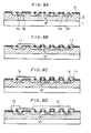
- Figs. 4A to 4C are sectional views showing a method of fabricating the power transistor according to the first embodiment. This method is now described with reference to these figures.
- the N + -type collector layer 1, the N - -type collector layer 2, the P-type well region 3, the N + -type emitter regions 4 and the low-resistance region 10 are formed by well-known methods.
- the low-resistance region 10 is simultaneously formed with the N + -type emitter regions 4.
- An oxide film is formed over the entire surface and then etched to define the oxide films 5 in the regions close to the boundaries between the N + -type emitter regions 4 and the P-type well region 3 and over the N - -type collector layer 2 at the end portions of the P-type well region 3, as shown in Fig. 4A.
- an aluminum layer is formed over the entire surface by vacuum deposition and subjected to selective etching to leave parts thereof on the region (6a) extending over the parts of the P-type well region 3 held between the oxide films 5 and parts of the said oxide films 5 as well as on the region (6b) extending over the parts of the P-type well region 3 held between the oxide films 5 and the low-resistance region 10 as well as the oxide films 5 and the parts of the low-resistance region 10, thereby forming the base electrode 6 as shown in Fig. 4B.
- interlayer insulation film 9 is generally prepared from polyimide, the material therefor is not restricted to polyimide but may be prepared from glass having a low melting point, for example, which can be formed at a temperature below that employed in a step of forming an aluminum electrode.
- the power transistor thus fabricated has a two-layer electrode structure
- the emitter electrode 7 and the base bonding electrode 8 corresponding to upper layer regions are directly in contact with the N + -type emitter regions 4 and the P-type well region 3 respectively. Therefore, it is not necessary to consider electrical barriers in contact portions between two-layer electrodes.
- a power transistor having a multilayer electrode structure can be formed with no function degradation by the vacuum deposition process, which is capable of high-speed processing at a low cost as compared with the sputtering process which is costly and takes much time.
- a contact region of two-layer electrodes is partially defined between the base electrode 6 and the base bonding electrode 8, to cause an electrical barrier similarly to the prior art when the base bonding electrode 8 is formed by vacuum deposition.
- this barrier can be regarded as not very problematic for the following reasons:
- the base electrode 6 and the base bonding electrode 8 can be maintained in sufficient electrical connection through the surface region of the P-type well region 3, even if the low-resistance region 10 is omitted.
- Figs. 5, 6 and 7 illustrate related devices, but their manufacture does not fall under the terms of the appended claims.
- Oxide films 5 are formed on a region over a surface part of the N - -type collector layer 2 (right-hand side in Fig. 5B) and a part of the P-type well region 3a, on regions close to boundaries between the P-type well region 3a and the N + -type emitter regions 4a, on regions over the P-type well region 3a and regions close to boundaries between the P-type well region 3b and the N + -type emitter regions 4b through a surface part of the N - -type collector layer 2, on regions close to the boundaries between the N + -type emitter regions 4b and the P-type well region 3b and on a region over the P-type well region 3b and the surface of the N - -type collector layer 2.
- An interlayer insulation film 9 is formed to cover the base/emitter electrode 11.
- An emitter electrode 12 of the transistor Qa is formed on a tetragonal region including the overall N + -type emitter regions 4a to be in contact with the N + -type emitter regions 4a, while a base electrode 13 of the transistor Qb is formed on a part 3b' of the P-type well region 3b. These electrodes 12 and 13 also serve as bonding regions.
- Fig. 5C is an equivalent circuit diagram of the transistors Qa and Qb shown in Figs. 5A and 5B.
- the base/emitter electrode 11 electrically connects the base and the emitter of the transistors Qa and Qb which are adjacent to each other, while the emitter electrode 12 serves as the emitter electrode of the transistor Qa of the final stage (second stage) capable of external connection by bonding and the base electrode 13 serves as the base electrode of the transistor Qb capable of external connection by bonding.
- Figs. 6A to 6D are sectional views showing a method of fabricating the power transistor but not according to the appended claims. With reference to these figures, the fabrication method will now be described.
- the N + -type collector layer 1, the N - -type collector layer 2, the P-type well regions 3a and 3b and the N + -type emitter regions 4a and 4b are formed by well-known fabrication methods. Then, the aforementioned oxide films 5 are selectively formed as shown in Fig. 6A.
- An aluminum layer is again formed over the entire surface by vacuum deposition and subjected to etching processing, thereby forming the emitter electrode 12 and the base electrode 13 of the aforementioned configurations, as shown in Fig. 6D.
- the emitter electrode 12 and the base electrode 13 corresponding to upper layer regions are directly in contact with the emitter regions 4a and the P-type well region 3b respectively, although the power transistor has a two-layer structure.
- a power transistor having a two-stage Darlington-connected structure can be formed by vacuum deposition with no function degradation.
- Fig. 7A is a plan view showing a power transistor having a four-stage Darlington-connected structure
- Fig. 7B is a sectional view taken along the line C5 - C5 in Fig. 7A.
- an N - -type collector layer 2 is formed on an N + -type collector layer 1.
- P-type well regions 3a to 3d are formed on an upper layer part of the N - -type collector layer 2, to serve as base regions of transistors Qa to Qb respectively.
- Pluralities of N + -type emitter regions 4a to 4d are formed on partial regions of the P-type well regions 3a to 3d respectively.
- Oxide films 5 are selectively formed on the following regions:
- An interlayer insulation film 9 is formed to cover the base/emitter electrodes 11 and 14.
- An emitter electrode 12 of the transistor Qa is formed on a tetragonal region including the N + -type emitter regions 4a to be in contact with the N + -type emitter regions 4a.
- a base electrode 15 of the transistor Qd is formed on a part 3d' of the P-type well region 3d.
- a base/emitter electrode 16 connecting the base of the transistor Qb with the emitter of the transistor Qc is formed over a part 3b' of the P-type well region 3b and the N + -type emitter regions 4c.
- a partial region 15' of the base electrode 15 serves as a bonding region.
- Fig. 7C is an equivalent circuit diagram of the power transistor having the aforementioned four-stage Darlington-connected structure.
- the base/emitter electrodes 11, 14 and 16 electrically connect the bases and the emitters of the adjacent pairs of transistors, while the emitter electrode 12 serves as the emitter electrode of the transistor in the final stage (fourth stage) capable of external connection by bonding and the base electrode 15 serves as the base electrode of the first stage transistor Qd capable of external connection by bonding.
- a detailed description of a method of fabricating the power transistor having a four-stage Darlington-connected structure is omitted since the same is substantially similar to that of fabricating the power transistor having a two-stage Darlington-connected structure.
- the base/emitter electrodes 11 and 14 are formed in a first electrode forming step, and the emitter electrode 12, the base/emitter electrode 16 and the base electrode 15 are formed in a second electrode forming step.
- the emitter electrode 12, the base/emitter electrode 16 and the base electrode 15 corresponding to upper layer regions are directly in contact with the emitter regions 4a, the base region 3b' and the emitter regions 4c, and the base region 3d' respectively, although the power transistor has a two-layer electrode structure.
- a power transistor having a four-stage Darlington-connected structure can be formed by vacuum deposition with no function degradation.
- Fig. 9A is a plan view showing a power transistor having a two-stage Darlington-connected structure, provided with a bonding electrode also in a base/emitter electrode and fabricated according to another embodiment of the present invention
- Figs. 9B and 9C are sectional views taken along the lines C6 - C6 and C7 - C7 in Fig. 9A respectively.
- this power transistor is basically similar in structure to the power transistor having a two-stage Darlington-connected structure as shown in Figs. 5A and 5B.
- a base/emitter bonding electrode 17 is formed on a part 3a" of a base region 3a and on a part 11' of a base/emitter electrode 11, in order to provide a bonding electrode also on an electrode electrically connecting the base of a transistor Qa with the emitter of another transistor Qb.
- the base/emitter bonding electrode 17 is formed over the base region 3a" within a low-resistance region 10 which is selectively provided in the base region 3a and the base/emitter electrode 11', not to be electrically in contact with an emitter electrode 12 of the transistor Qa and a base electrode 13 of the transistor Qb.
- Fig. 9D is an equivalent circuit diagram of the power transistor having the aforementioned two-stage Darlington-connected structure.
- the base/emitter electrode 11 electrically connects the base and the emitter of the transistors Qa and QB, while the emitter electrode 12 serves as the emitter electrode of the transistor in the final stage (second stage) capable of an external connection by bonding and the base electrode 13 serves as the base electrode of the first stage transistor Qb capable of an external connection by bonding.
- the base/emitter bonding electrode 17 serves as the bonding electrode of the base/emitter electrode 11.
- Figs. 10A to 10D and 11A to 11D show a method of fabricating the power transistor according to this second embodiment.
- Figs. 10A to 10D are sectional views taken along the line C6 - C6 in Fig. 9A
- Figs. 11A to 11D are sectional views taken along the line C7 - C7 in Fig. 9A.
- the N + -type collector layer 1, the N -type collector layer 2, the P-type well regions 3a and 3b, the N + -type emitter regions 4a and 4b and the low-resistance region 10 are formed by well-known fabrication methods.
- the low-resistance region 10 is formed simultaneously with the N + -type emitter regions 4a and 4b.
- oxide films 5 are formed on a region over the N - -type collector layer 2 and an end portion of the P-type well region 3a, regions close to boundaries between the P-type well region 3a and the N + -type emitter regions 4a, regions over another end portion of the P-type well region 3a and regions close to boundaries between the P-type well region 3b and the N + -type emitter regions 4b or an end portion of the P-type well region 3b through the N - -type collector layer 2, regions close to the boundaries between the P-type well region 3b and the N + -type emitter regions 4b and a region over another end portion of the P - -type well region 3b and the N - -type collector layer 2, as shown in Figs. 10A and 11A.
- an aluminum layer is formed over the entire surface by vacuum deposition and selectively etched to leave portions of the aluminum layer on a portion of the P-type well region 3a excluding the region 3a" enclosed by the low-resistance region 10a and regions over a part 3a' of the P-type well region 3a and the N + -type emitter regions 4b, thereby forming the base/emitter electrode 11 as shown in Figs. 10B and 11B.
- An insulating film is formed over the entire surface and selectively etched to leave a portion covering the base/emitter electrode 11, thereby forming the interlayer insulation film 9 as shown in Figs. 10C and 11C. At this time, the interlayer insulation film 9 is formed to be exposed by about half in a part 11' of the base/emitter electrode 11.
- An aluminum layer is again formed by vacuum deposition and etched to form the emitter electrode 12 on the N + -type emitter regions 3a, the base/emitter bonding electrode 17 on the portion 3a" of the P-type well region 3a and the portion 11' of the base/emitter electrode 11, and the base electrode 13 on the P-type base region 3b respectively.
- the power transistor fabricated in the aforementioned manner also has the bonding electrode on the electrode between the base and the emitter of the transistors Qa and Qb, whereby a speed-up diode D1, which is fed back from the base of the transistor Qa to that of the transistor Qb, can be externally provided.
- An electrical barrier defined in a contact portion between the base/emitter bonding electrode 17 and the base/emitter electrode 11' substantially causes no problem similarly to the electrical barrier defined in the contact portion between the base bonding electrode 8 and the base electrode 6b in the first embodiment.
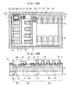
- Fig. 12A is a plan view showing a power transistor having a three-stage Darlington-connected structure which is fabricated with bonding electrodes also on base/emitter electrodes according to the third embodiment of the present invention
- Figs. 12B and 12C are sectional views taken along the lines C8 - C8 and C9 - C9 in Fig. 12A respectively.
- an N - -type collector layer 2 is formed on an N + -type collector layer 1.
- P-type well regions 3a to 3c are formed on an upper layer part of the N - -type collector layer 2 to serve as base regions of transistors Qa to Qc respectively.
- a plurality of N + -type emitter regions 4a to 4c are formed on surface portions of the P-type well regions 3a to 3c respectively.
- Low-resistance regions 10a and 10c are provided in the form of rings on surface parts of the P-type well regions 3a and 3c respectively.
- Oxide films 5 are selectively formed on the following regions:
- a base electrode 21 of the transistor Qc is formed on the P-type well region 3c excluding a region 3c" enclosed by the ring-shaped low-resistance region 10c.
- An interlayer insulation film 9 is formed to cover the electrodes 11 and 21, to be exposed by about half in parts 11' and 21' of the electrodes 11 and 21.
- An emitter electrode 12 of the transistor Qa is formed on a region including the overall N + -type emitter regions 4a and the interlayer insulation film 9 formed between the N + -type emitter regions 4a.
- a base/emitter bonding electrode 18 is formed on the part 3a" of the P-type well region 3a and the part 11' of the base electrode 11, while another base bonding electrode 20 is formed on the part 3c" of the P-type well region 3c and the part 21' of the base electrode 21. Further, a base/emitter electrode 19, which electrically connects the base of the transistor Qb with the emitter of the transistor Qc, is formed over the P-type well region 3b and the N + -type emitter regions 4c. A portion 19' of the base/emitter electrode 19 serves as a bonding electrode.
- Fig. 12D is an equivalent circuit diagram showing the power transistor having the aforementioned three-stage Darlington-connected structure.
- the base/emitter electrodes 11 and 19 electrically connect the bases and the emitters of the adjacent pairs of transistors, while the emitter electrode 12 serves as the emitter electrode of the transistor Qa in the final stage (third stage) capable of an external connection by bonding.
- the base/emitter bonding electrode 18 and the part 19' of the base/emitter electrode 19 serve as external terminal connecting regions between the bases and the emitters of the transistors Qa and Qb as well as Qb and Qc.
- the base electrode 21 and the base bonding electrode 20 serve as the base electrode of the transistor Qc having an externally connectable bonding region.
- the base/emitter electrode 11 and the base electrode 21 are formed in a first electrode forming step (corresponding to the step shown in Figs. 10B and 11B), while the emitter electrode 12, the base/emitter bonding electrode 18, the base/emitter electrode 19 and the base bonding electrode 20 are formed in a second electrode/bonding electrode forming step (corresponding to the step shown in Figs. 10D and 11D).
- the bonding electrodes can be provided between the bases and the emitters of the adjacent pairs of transistors also in the power transistor having a three-stage Darlington-connected structure, whereby speed-up diodes D1 and D2, which are fed back from the bases of the transistors Qa and Qb to the bases of the transistors Qb and Qc respectively, can be externally provided.
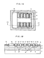
- Fig. 13A is a plan view showing a power transistor having four-stage Darlington-connected structure which is fabricated with bonding regions also in base/emitter electrodes according to the fourth embodiment of the present invention
- Figs. 13B and 13C are sectional views taken along the lines C10 - C10 and C11 - C11 in Fig. 13A respectively.
- an N - -type collector layer 2 is formed on an N + -type collector layer 1.
- P-type well regions 3a to 3d are formed on an upper layer part of the N - -type collector layer 2, to serve as base regions of transistors Qa to Qd respectively.
- a plurality of N + -type emitter regions 4a to 4d are formed on partial regions of the surfaces of the P-type well regions 3a to 3d respectively.
- Ring-shaped low-resistance regions 10a and 10c are formed on surface parts of the P-type well regions 3a and 3c respectively.
- Oxide films 5 are selectively formed on the following regions:
- another base/emitter electrode 22 which is an electrode electrically connecting the base of the transistor Qc and the emitter of the transistor Qd, is formed on the P-type well region 3c excluding a region 3c" enclosed by the ring-shaped low-resistance region 10c and over a part 3c' of the P-type well region 3c and the N + -type emitter regions 4d.
- An interlayer insulation film 9 is formed to cover the electrodes 11 and 12 and to be exposed by about half in parts 11'and 22' of the electrodes 11 and 12.
- a base/emitter bonding electrode 23 is formed on the part 3a" of the P-type well region 3a and the part 11' of the base electrode 11, and another base/emitter bonding electrode 25 is formed on the part 3c" of the P-type well region 3c and the part 22' of the base/emitter electrode 22.
- still another base/emitter electrode 24 is formed on regions over the P-type well region 3b and the N + -type emitter regions 4c and on the interlayer insulation film 9 provided on the N + -type emitter regions 4b, while a base electrode 26 is formed on the P-type well region 3d and the interlayer insulation film 9 provided on the N + -type emitter regions 4d.
- a portion 24' of the base/emitter electrode 24 serves as a bonding electrode.
- Fig. 13D is an equivalent circuit diagram showing the transistor having the aforementioned four-stage Darlington-connected structure.
- the base/emitter electrodes 11, 24 and 22 electrically connect the bases and the emitters of the adjacent pairs of transistors, while the emitter electrode 12 serves as the emitter electrode of the transistor Qa in the final stage (fourth stage) capableofanexternal connection by bonding.
- the base electrode 26 serves as the base electrode of the first stage transistor Qd.
- the base/emitter bonding electrode 23, the portion 24' of the base/emitter electrode 24 and the base/emitter bonding electrode 25 serve as external terminal connecting bonding electrodes of the bases and the emitters of the transistors Qa and Qb, Qb and Qc, as well as Qc and Qd.
- the base/emitter electrodes 11 and 22 are formed in a first electrode forming step (corresponding to the step shown in Figs. 10B and 11B), and the base/emitter bonding electrodes 23 and 25, the base/emitter electrode 24 and the base electrode 26 are formed in a second electrode/bonding electrode forming step (corresponding to the step shown in Figs. 10D and 11D).
- the bonding electrodes are provided between the bases and the emitters of the adjacent pairs of transistors in the power transistor having the aforementioned four-stage Darlington-connected structure, whereby speed-up diodes D1 to D3 can be externally provided between the transistors Qa and Qb, Qb and Qc, and Qc and Qd respectively as shown in Fig. 13D.
- Figs. 15, 16 and 17 illustrate other devices which however are not fabricated under the present method as defined in the appended claims.
- Fig. 15A is a plan view showing another power transistor having a two-stage Darlington-connected structure
- Fig. 15B is a sectional view taken along the line C12 - C12 in Fig. 15A.
- This power transistor is basically similar in structure to the power transistor having the two-stage Darlington-connected structure shown in Figs. 9A - 9D.
- the power transistor contains a speed-up diode D1 formed between the base of a transistor Qa and the base of a transistor Qb.
- a part of a base electrode 13 of the transistor Qb is provided extendedly over a P-type well region 3a of the transistor Qa, and an N + -type diffusion region 70 is provided on the surface of the P-type well region 3a under the base electrode 13.
- the speed-up diode D1 is formed between the base of the transistor Qa and the base of the transistor Qb by the PN junction of the P-type well region 3a and the N + -type diffusion region 70.
- the PN junction of the P-type well region 3a and the N + -type diffusion region 70 behave not only as a diode but also as a parasitic transistor with an N + -type collector layer 1 and an N - -type collector layer 2, and thereby has a parasitic transistor operation.
- it is effective to reduce a current amplification efficiency h FE of the parasitic transistor by carrying out parasitic transistor restraint measures of decreasing the density of the N + -type diffusion region 70, increasing the density of the P-type well region 3a around the N + -type diffusion region 70.
- Fig. 16A is a plan view showing a power transistor having a three-stage Darlington-connected structure according to another comparative example and Fig. 16B is a sectional view taken along the line C13 - C13 in Fig. 16A.
- This power transistor is basically similar in structure to the power transistor having a three-stage Darlington-connected structure.
- This comparative power transistor contains speed-up diodes D1 and D2 which are fed back from the bases of transistors Qa and Qb to the bases of transistors Qb and Qc respectively.
- a part of a base/emitter electrode 19 of the transistors Qb and Qc is provided extendedly over a P-type well region 3a of the transistor Qa, and an N + -type diffusion region 70 is provided on the surface of the P-type well region 3a under the base/emitter electrode 19.
- a part of a base electrode 21 of the transistor Qc is provided extendedly over a P-type well region 3b, and an N + -type diffusion region 71 is provided on the surface of the P-type well region 3b under the base electrode 21.
- the speed-up diode D1 is formed between the base of the transistor Qa and the base of the transistor Qb by the PN junction of the P-type well region 3a and the N + -type diffusion region 70.
- the speed-up diode D2 is formed between the base of the transistor Qb and the base of the transistor Qc by the PN junction of the P-type well region 3b and the N + -type diffusion region 71.
- Fig. 17A is a plan view showing a power transistor having a four-stage Darlington-connected structure according to another comparative example and Fig. 17B is a sectional view taken along the line C14 - C14 in Fig. 17A.
- This power transistor is basically similar in structure to the power transistor having the four-stage Darlington-connected structure according to the fourth embodiment shown in Figs. 13A - 13D.
- the comparative power transistor contains speed-up diodes D1, D2 and D3 which are fed back from the bases of transistors Qa, Qb and Qc to the bases of transistors Qb, Qc and Qd respectively.
- a part of a base/emitter electrode 24 of the transistors Qb and Qc is provided extendedly over a P-type well region 3a of the transistor Qa, and an N + -type diffusion region 70 is provided on the surface of the P-type well region 3a under the base/emitter electrode 24.
- a part of a base/emitter electrode 22 of the transistors Qc and Qd is provided extendedly over a P-type well region 3b of the transistor Qb, and an N + -type diffusion region 71 is provided on the surface of the P-type well region 3b under the base/emitter electrode 22.
- a part of a base electrode 26 of the transistor Qd is provided extendedly over a P-type well region 3c, and an N + -type diffusion region 72 is provided on the surface of the P-type well region 3c under the base electrode 26.
- the speed-up diode D1 is formed between the base of the transistor Qa and the base of the transistor Qb by the PN junction of the P-type well region 3a and the N + -type diffusion region 70.
- the speed-up diode D2 is formed between the base of the transistor Qb and the base of the transistor Qc by the PN junction of the P-type well region 3b and the N + -type diffusion region 71.
- the speed-up diode D3 is formed between the base of the transistor Qc and the base of the transistor Qd by the PN junction of the P-type well region 3c and the N + -type diffusion region 72.
- the present invention is also applicable to a power transistor having a Darlington-connected structure including five or more stages by modifying the aforementioned embodiments. It is of course possible to form also a bonding electrode between the base and the emitter of an adjacent pair of transistors. Further, the present invention is not restricted to any power transistor but is also applicable to a general thyristor, a gate turn off thyristor (GTO) or the like.
- GTO gate turn off thyristor
- numeral 51 denotes a P-type substrate
- numeral 52 denotes an N + -type buffer layer
- numeral 53 denotes an N-type semiconductor layer
- numeral 54 denotes a P-type well region
- numeral 55 denotes an N-type diffusion region
- numeral 56 denotes a low-resistance region
- numerals 57 and 60 denote gate electrodes
- numeral 58 denotes an interlayer insulation film
- numeral 59 denotes an anode electrode
- numeral 61 denotes a cathode electrode.
- a second-layer electrode including a bonding electrode
- Such an electrode may be formed in a comb-like pattern similarly to the base electrode 13 (see Fig. 9) of the second embodiment, or in overlay structure.
- a preferable result is expected in the overlay structure in view of current supply ability, while the proportion defective is disadvantageously increased in this case since the structure is complicated. Supposing from the above reason, it may be preferable to form the emitter electrode (the emitter electrode 12 of Fig. 13, for example) of the final stage, having the highest current density, in overlay structure while forming other electrodes in comb-like patterns in Darlington-connected transistors.
- the present invention is not restricted to this and the emitter electrode may also be provided in the form of a lattice or mesh so far as the configuration is adapted to expand an effective operating region.
- the base electrode of the final stage transistor is not restricted to the comb-like configuration shown in each embodiment.
- electrode connecting portions of an emitter region may also he formed discretely so that the base electrode can be provided on the emitter region, which is not an electrode connecting portion, through an oxide film to expand a base electrode forming area, thereby to increase base current supply ability.
Landscapes
- Bipolar Integrated Circuits (AREA)
- Bipolar Transistors (AREA)
Claims (5)
- Verfahren zum Herstellen einer Halbleitervorrichtung, wobei das Verfahren die folgende Abfolge von Schritten aufweist:- Herstellen einer ersten Halbleiterschicht (2, 52, 53) eines ersten Leitfähigkeits-Typs, die eine erste und eine zweite Hauptfläche aufweist;- selektives Bilden eines ersten Halbleiterbereichs (3, 3a, 3a', 3a", 54) eines zweiten Leitfähigkeits-Typs auf der ersten Hauptfläche der ersten Halbleiterschicht;- selektives Bilden eines zweiten Halbleiterbereichs (4, 4a, 55) des ersten Leitfähigkeits-Typs auf dem ersten Halbleiterbereich;- Bilden einer ersten Elektrode (6, 6a, 6b, 11, 11', 57) mit einem ersten Bereich (6a, 11, 57) und einem zweiten Bereich (6b, 11', 57) auf einem Teil des ersten Halbleiterbereichs, ausgenommen einen anderen Teil (3', 3") des ersten Halbleiterbereichs sowie nicht in direktem Kontakt mit dem zweiten Halbleiterbereich;- Bilden einer Isolierschicht (5, 9, 9', 58) auf der gesamten Oberfläche der resultierenden Vorrichtung;- selektives Ätzen der Isolierschicht derart, daß der erste Bereich der ersten Elektrode bedeckt ist, jedoch nicht ein Teil des zweiten Bereiches der ersten Elektrode;- Bilden einer zweiten Elektrode (7, 12, 59) auf dem zweiten Halbleiterbereich und der Isolierschicht, und zwar getrennt von der ersten Elektrode;- Bilden, durch einen Vakuumdampfabscheidungsprozeß, einer dritten Elektrode (8, 17, 23, 60) auf dem anderen Teil (3', 3a") des ersten Halbleiterbereichs, auf dem die erste Elektrode nicht vorgesehen ist, sowie auf dem Teil des zweiten Bereichs der ersten Elektrode, der nicht von der Isolierschicht bedeckt ist.
- Verfahren nach Anspruch 1,
das folgende weiteren Schritte aufweist:- selektives Bilden eines Bereichs (10, 10a, 56) mit niedrigem Widerstand auf der Oberfläche des ersten Halbleiterbereichs getrennt von dem zweiten Halbleiterbereich;- Bilden der ersten Elektrode auch auf einem Teil des Bereichs mit niedrigem Widerstand; und- Bilden der dritten Elektrode auch auf dem Teil des Bereichs mit niedrigem Widerstand, der nicht mit der ersten Elektrode versehen ist. - Verfahren nach einem der Ansprüche 1 oder 2,
das folgende weiteren Schritte aufweist:- Bilden einer zweiten Halbleiterschicht (51) des zweiten Halbleiter-Typs auf der zweiten Hauptfläche der ersten Halbleiterschicht (52, 53); und- Bilden einer vierten Elektrode (61) auf der zweiten Halbleiterschicht (51). - Verfahren nach einem der Ansprüche 1 bis 3,
das folgende weiteren Schritte aufweist:- selektives Bilden eines dritten Halbleiterbereichs (3b) des zweiten Leitfähigkeits-Typs auf der ersten Halbleiterschicht getrennt von dem ersten Halbleiterbereich;- selektives Bilden eines vierten Halbleiterbereichs (4b) des ersten Leitfähigkeits-Typs auf dem dritten Halbleiterbereich;- Bilden der ersten Elektrode auch auf dem vierten Halbleiterbereich; und- Bilden einer weiteren Elektrode (13) auf dem dritten Halbleiterbereich und der Isolierschicht getrennt von der zweiten Elektrode (12). - Verfahren nach einem der Ansprüche 1 bis 4,
wobei die zweite Elektrode in einer Overlay-Struktur gebildet wird.
Applications Claiming Priority (4)
| Application Number | Priority Date | Filing Date | Title |
|---|---|---|---|
| JP255926/89 | 1989-09-29 | ||
| JP25592689 | 1989-09-29 | ||
| JP2241418A JP2521840B2 (ja) | 1989-09-29 | 1990-09-11 | 半導体装置及びその製造方法 |
| JP241418/90 | 1990-09-11 |
Publications (2)
| Publication Number | Publication Date |
|---|---|
| EP0420164A1 EP0420164A1 (de) | 1991-04-03 |
| EP0420164B1 true EP0420164B1 (de) | 1997-12-10 |
Family
ID=26535250
Family Applications (1)
| Application Number | Title | Priority Date | Filing Date |
|---|---|---|---|
| EP90118419A Expired - Lifetime EP0420164B1 (de) | 1989-09-29 | 1990-09-25 | Verfahren zur Herstellung einer Halbleiteranordnung mit mehrschichtiger Elektrodenstruktur |
Country Status (3)
| Country | Link |
|---|---|
| US (1) | US5111267A (de) |
| EP (1) | EP0420164B1 (de) |
| DE (1) | DE69031795T2 (de) |
Families Citing this family (3)
| Publication number | Priority date | Publication date | Assignee | Title |
|---|---|---|---|---|
| EP0675527B1 (de) * | 1994-03-30 | 1999-11-10 | Consorzio per la Ricerca sulla Microelettronica nel Mezzogiorno | Verfahren zur Herstellung von bipolaren Transistoren mit kontrollierter Speicherzeit |
| JP2946306B2 (ja) * | 1995-09-12 | 1999-09-06 | セイコーインスツルメンツ株式会社 | 半導体温度センサーとその製造方法 |
| US6498561B2 (en) * | 2001-01-26 | 2002-12-24 | Cornerstone Sensors, Inc. | Thermistor and method of manufacture |
Family Cites Families (5)
| Publication number | Priority date | Publication date | Assignee | Title |
|---|---|---|---|---|
| US3619738A (en) * | 1969-10-13 | 1971-11-09 | Tokyo Shibaura Electric Co | Semiconductor device with improved connection to control electrode region |
| JPS5268376A (en) * | 1975-12-05 | 1977-06-07 | Nec Corp | Semiconductor device |
| JPS59104165A (ja) * | 1982-12-06 | 1984-06-15 | Mitsubishi Electric Corp | 電力用トランジスタ |
| US4646125A (en) * | 1983-07-27 | 1987-02-24 | Mitsubishi Denki Kabushiki Kaisha | Semiconductor device including Darlington connections |
| EP0266205B1 (de) * | 1986-10-31 | 1993-12-15 | Nippondenso Co., Ltd. | Bipolarer Halbleitertransistor |
-
1990
- 1990-09-18 US US07/584,059 patent/US5111267A/en not_active Expired - Fee Related
- 1990-09-25 EP EP90118419A patent/EP0420164B1/de not_active Expired - Lifetime
- 1990-09-25 DE DE69031795T patent/DE69031795T2/de not_active Expired - Fee Related
Non-Patent Citations (1)
| Title |
|---|
| International Electron Devices Meeting (IEDM), Technical Digest, December 1985, pp. 142-145 (Miller et al.) * |
Also Published As
| Publication number | Publication date |
|---|---|
| EP0420164A1 (de) | 1991-04-03 |
| DE69031795T2 (de) | 1998-06-18 |
| DE69031795D1 (de) | 1998-01-22 |
| US5111267A (en) | 1992-05-05 |
Similar Documents
| Publication | Publication Date | Title |
|---|---|---|
| US5286655A (en) | Method of manufacturing a semiconductor device of an anode short circuit structure | |
| US4127863A (en) | Gate turn-off type thyristor with separate semiconductor resistive wafer providing emitter ballast | |
| EP0420164B1 (de) | Verfahren zur Herstellung einer Halbleiteranordnung mit mehrschichtiger Elektrodenstruktur | |
| US5229313A (en) | Method of making a semiconductor device having multilayer structure | |
| JPH06103745B2 (ja) | 集積回路素子 | |
| JPH08264762A (ja) | 化合物半導体装置及びその製造方法 | |
| JP2974583B2 (ja) | 半導体装置およびその製造方法 | |
| CA1205577A (en) | Semiconductor device | |
| US20050092981A1 (en) | Superconducting integrated circuit and methods of forming same | |
| JPH07235660A (ja) | サイリスタの製造方法 | |
| JPH08130317A (ja) | 抵抗性フィ−ルドプレ−トを備えた半導体装置 | |
| JP2521840B2 (ja) | 半導体装置及びその製造方法 | |
| JPH05304289A (ja) | 半導体装置 | |
| JPS61187271A (ja) | ヘテロ接合型バイポ−ラトランジスタ | |
| JP3278498B2 (ja) | 絶縁ゲート型電力用半導体装置 | |
| KR19990010738A (ko) | 전력용 반도체소자 및 그 제조방법 | |
| JPH0680817B2 (ja) | 半導体装置 | |
| JPH065935A (ja) | 超電導体装置 | |
| JPS62189752A (ja) | 半導体装置 | |
| JPH0669092B2 (ja) | ゲ−トタ−ンオフサイリスタの製造方法 | |
| JPH04357841A (ja) | バイポーラ・トランジスタの構造および製造方法 | |
| JPH07297413A (ja) | 酸化物負性抵抗素子とその製造方法 | |
| JPH0629518A (ja) | 半導体装置 | |
| JPS58210659A (ja) | 半導体装置およびその製造方法 | |
| JPH0618269B2 (ja) | シヨツトキバリア半導体装置 |
Legal Events
| Date | Code | Title | Description |
|---|---|---|---|
| PUAI | Public reference made under article 153(3) epc to a published international application that has entered the european phase |
Free format text: ORIGINAL CODE: 0009012 |
|
| 17P | Request for examination filed |
Effective date: 19901212 |
|
| AK | Designated contracting states |
Kind code of ref document: A1 Designated state(s): DE FR GB SE |
|
| 17Q | First examination report despatched |
Effective date: 19950530 |
|
| GRAG | Despatch of communication of intention to grant |
Free format text: ORIGINAL CODE: EPIDOS AGRA |
|
| GRAH | Despatch of communication of intention to grant a patent |
Free format text: ORIGINAL CODE: EPIDOS IGRA |
|
| GRAH | Despatch of communication of intention to grant a patent |
Free format text: ORIGINAL CODE: EPIDOS IGRA |
|
| GRAA | (expected) grant |
Free format text: ORIGINAL CODE: 0009210 |
|
| AK | Designated contracting states |
Kind code of ref document: B1 Designated state(s): DE FR GB SE |
|
| REF | Corresponds to: |
Ref document number: 69031795 Country of ref document: DE Date of ref document: 19980122 |
|
| ET | Fr: translation filed | ||
| REG | Reference to a national code |
Ref country code: GB Ref legal event code: 727 |
|
| REG | Reference to a national code |
Ref country code: GB Ref legal event code: 727A |
|
| PGFP | Annual fee paid to national office [announced via postgrant information from national office to epo] |
Ref country code: SE Payment date: 19980904 Year of fee payment: 9 |
|
| PGFP | Annual fee paid to national office [announced via postgrant information from national office to epo] |
Ref country code: FR Payment date: 19980909 Year of fee payment: 9 |
|
| REG | Reference to a national code |
Ref country code: GB Ref legal event code: 727B |
|
| REG | Reference to a national code |
Ref country code: GB Ref legal event code: SP |
|
| PGFP | Annual fee paid to national office [announced via postgrant information from national office to epo] |
Ref country code: GB Payment date: 19981001 Year of fee payment: 9 |
|
| PGFP | Annual fee paid to national office [announced via postgrant information from national office to epo] |
Ref country code: DE Payment date: 19981005 Year of fee payment: 9 |
|
| PLBE | No opposition filed within time limit |
Free format text: ORIGINAL CODE: 0009261 |
|
| STAA | Information on the status of an ep patent application or granted ep patent |
Free format text: STATUS: NO OPPOSITION FILED WITHIN TIME LIMIT |
|
| 26N | No opposition filed | ||
| PG25 | Lapsed in a contracting state [announced via postgrant information from national office to epo] |
Ref country code: GB Free format text: LAPSE BECAUSE OF NON-PAYMENT OF DUE FEES Effective date: 19990925 |
|
| PG25 | Lapsed in a contracting state [announced via postgrant information from national office to epo] |
Ref country code: SE Free format text: THE PATENT HAS BEEN ANNULLED BY A DECISION OF A NATIONAL AUTHORITY Effective date: 19990929 |
|
| EUG | Se: european patent has lapsed |
Ref document number: 90118419.2 |
|
| GBPC | Gb: european patent ceased through non-payment of renewal fee |
Effective date: 19990925 |
|
| PG25 | Lapsed in a contracting state [announced via postgrant information from national office to epo] |
Ref country code: FR Free format text: LAPSE BECAUSE OF NON-PAYMENT OF DUE FEES Effective date: 20000531 |
|
| PG25 | Lapsed in a contracting state [announced via postgrant information from national office to epo] |
Ref country code: DE Free format text: LAPSE BECAUSE OF NON-PAYMENT OF DUE FEES Effective date: 20000701 |
|
| REG | Reference to a national code |
Ref country code: FR Ref legal event code: ST |