EP0420688A2 - System zum Auslöschung von Geisterbildern und Steuerverfahren dafür - Google Patents
System zum Auslöschung von Geisterbildern und Steuerverfahren dafür Download PDFInfo
- Publication number
- EP0420688A2 EP0420688A2 EP90310677A EP90310677A EP0420688A2 EP 0420688 A2 EP0420688 A2 EP 0420688A2 EP 90310677 A EP90310677 A EP 90310677A EP 90310677 A EP90310677 A EP 90310677A EP 0420688 A2 EP0420688 A2 EP 0420688A2
- Authority
- EP
- European Patent Office
- Prior art keywords
- signal
- reference signal
- ghost
- gcr
- waveform
- Prior art date
- Legal status (The legal status is an assumption and is not a legal conclusion. Google has not performed a legal analysis and makes no representation as to the accuracy of the status listed.)
- Withdrawn
Links
- 238000000034 method Methods 0.000 title claims description 8
- 238000004422 calculation algorithm Methods 0.000 claims abstract description 9
- 238000000605 extraction Methods 0.000 claims description 33
- 238000001514 detection method Methods 0.000 claims description 20
- 238000004364 calculation method Methods 0.000 claims description 17
- 238000006243 chemical reaction Methods 0.000 claims description 5
- 239000000284 extract Substances 0.000 abstract description 2
- 230000015654 memory Effects 0.000 description 30
- 238000012545 processing Methods 0.000 description 4
- 238000010276 construction Methods 0.000 description 3
- 238000012937 correction Methods 0.000 description 3
- 238000010586 diagram Methods 0.000 description 3
- 230000003111 delayed effect Effects 0.000 description 2
- 238000012986 modification Methods 0.000 description 2
- 230000004048 modification Effects 0.000 description 2
- 241000973887 Takayama Species 0.000 description 1
- 238000011161 development Methods 0.000 description 1
- 230000000694 effects Effects 0.000 description 1
- 230000003936 working memory Effects 0.000 description 1
Images


Classifications
-
- H—ELECTRICITY
- H04—ELECTRIC COMMUNICATION TECHNIQUE
- H04N—PICTORIAL COMMUNICATION, e.g. TELEVISION
- H04N5/00—Details of television systems
- H04N5/14—Picture signal circuitry for video frequency region
- H04N5/21—Circuitry for suppressing or minimising disturbance, e.g. moiré or halo
-
- H—ELECTRICITY
- H04—ELECTRIC COMMUNICATION TECHNIQUE
- H04N—PICTORIAL COMMUNICATION, e.g. TELEVISION
- H04N5/00—Details of television systems
- H04N5/14—Picture signal circuitry for video frequency region
- H04N5/21—Circuitry for suppressing or minimising disturbance, e.g. moiré or halo
- H04N5/211—Ghost signal cancellation
Definitions
- the present invention relates, in general, to a ghost cancelling system, and more particularly to a ghost cancelling system for cancelling ghost signals from a video signal using a reference signal of the 8-field sequence type.
- GCR ghost cancel reference
- the ghost signal is cancelled with the aid of a GCR signal inserted with a period of 8 fields in the 18th horizontal scanning line (18H) of the odd numbered fields and the 281st horizontal scanning line (281H) of the even numbered fields. Further, the ghost signal is detected using the finally calculated GCR signal (S GCR ) that is obtained by performing the 8-field sequence calculation indicated by the following equation (1).
- S GCR (S1 - S5) + (S6 - S2) + (S3 - S7) + (S8 -S4) (1)
- This operation is performed in order to remove the ghost effect of the horizontal scanning line signal previous to the horizontal scanning line in which the GCR signal is inserted, and the horizontal synchronization signal and color burst signal of the horizontal scanning line in which the GCR signal is inserted.
- a conventional ghost cancelling system using a GCR signal of the 8-field sequence type is described in Japanese Patent Disclosure (Kokai) No. 59-211315.
- the conventional ghost cancelling system in order to extract the GCR signals (S1) - (S8) corresponding to eight fields, it is necessary to detect the first GCR signal (S1) itself.
- the construction of an S1 line detector which detects the arrival of the first GCR signal (S1) is complicated. This is because, in order to detect the first GCR signal (S1) itself, the following three conditions must all be fulfilled.
- condition 1 the horizontal scanning line is the 18H horizontal scanning line
- condition 2 the GCR signal is a signal of waveform that rises steeply from black to white, then falls smoothly from white to black (hereafter, WRB (Wide Reverse Bar) waveform signal).
- condition 3 the phase of the color burst signal is positive polarity (+).
- condition 1 can be detected using an ordinary line detection technique.
- detection of conditions 2 and 3 requires complicated processing to ascertain the shapes of the respective waveforms and determine their phase. Therefore, this requirement to detect conditions 2 and 3 made the construction of the conventional S1 line detection means complicated, making the system costly.
- a ghost cancelling system including a transversal filter having a plurality of tapped delay lines, coefficient circuits, an adder and a tap coefficient memory, wherein the tapped delay lines operate as an input portion of the transversal filter and delay the input signal by a specified delay time, the tap coefficient memory maintains the value of each tap coefficient corresponding to the tapped delay lines, the coefficient circuits are connected to the corresponding delay lines and amplify the delayed output signal by the tap coefficients, and the adder sums the amplified output signals from the coefficient circuits and operates as an output portion of the transversal filter.
- a line detection device detects a horizontal scanning line in which the reference signal is inserted from the signal of the input portion or the output portion of the transversal filter.
- a reference signal extraction device extracts the reference signal over 8 fields, starting with the horizontal scanning line which is detected by the line detection device.
- a reference signal calculation device finds a final reference signal corresponding to the 8 field reference signals which are extracted by the reference signal extraction device, using a specified calculation algorithm.
- a ghost detection device detects the ghost signal using the final reference signal calculated by the reference signal calculation device.
- a tap coefficient calculation device calculates the tap coefficient of the transversal filter using the detection output of the ghost detection device.
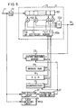
- the ghost cancelling system includes a transversal filter (hereafter, TF) 15, an analog /digital conversion circuit (hereafter, A/D conversion circuit) 12, a microprocessor 17, ROM 18, RAM 19 and an output waveform memory 20.
- ROM 18 is a memory element that stores the control program of microprocessor 17.
- RAM 19 is a memory element that is used as working memory.
- the output waveform memory 20 is used for writing the ghost cancelling output waveform in real time.
- the TF 15 includes a plurality of tapped delay lines 151, coefficient circuits 152 corresponding to the tapped delay lines 151, an adder 153 and a tap coefficient memory 154.
- the video signal containing the GCR signal is supplied through an input terminal 11 to the A/D conversion circuit 12, an 18H detection circuit 31 and a clock generating circuit 14.
- the digital video signal that is output from the A/D conversion circuit 12, which is operated by clock CK of period T is input to the TF 15 in order for the ghost signal to be cancelled from the video signal.
- the video signal that is input to the TF 15 is sequentially delayed with period T by the tapped delay lines 151.
- Each of the outputs of the tapped delay lines 151 is multiplied by a tap coefficient C -m - C n by a respective corresponding coefficient circuit 152. Then the results are added by the adder 153. This added output is supplied to an output terminal 16 and the output waveform memory 20 as the output of TF 15.
- the 18H detection circuit 31 detects the 18-th horizontal scanning line (18H).
- an extraction control circuit 21 instructs the microprocessor 17 and the output waveform memory 20 to perform waveform extraction to extract GCR signals for 8 fields continuously, starting with 18H.
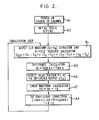
- Fig. 2 The operating sequence of this system is shown in Fig. 2.
- step A1 On power-up or when the channel is changed (step A1), initial state setting processing such as resetting to zero the tap coefficients C -m - C n that are latched in the tap coefficient memory 154 of the TF 15 is performed (step A2). After this, the equalization loop indicated in steps B-A8 is executed. The details of step B are shown in Fig. 3.
- step B1 the extraction of GCR signals for 8 fields continuously starts from 18H.
- the microprocessor 17 finds the final GCR signal (S GCR ) by executing the process from steps B2 to B17 of Fig. 3. This process for finding the final GCR signal (S GCR ) is described below.
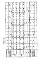
- the GCR signal (WRB waveform signal or black flat waveform signal) Y1 obtained by the first extraction is extracted into the output waveform memory 20, then stored in a waveform region ⁇ a ⁇ of the working RAM 19 (step B2).
- the address of a waveform region ⁇ a ⁇ is shown in the memory map of Fig. 4.
- the GCR signal Y2 obtained by the second extraction is extracted into the output waveform memory 20, then subtracted from the contents of waveform region ⁇ a ⁇ .
- the result of this subtraction (Y1 - Y2) is stored in the waveform region ⁇ a ⁇ .
- step B4 the GCR signal Y3 obtained by the third extraction is extracted into the output waveform memory 20, then stored in a waveform region ⁇ b ⁇ of the working RAM 19.
- the address of the waveform region ⁇ b ⁇ is shown in the memory map of Fig. 4.
- step B5 the GCR signal Y4 obtained by the fourth extraction is extracted into the output waveform memory 20, then subtracted from the contents of the waveform region ⁇ b ⁇ .
- the result of this subtraction (Y3 - Y4) is stored in the waveform region ⁇ b ⁇ .
- step B6 the GCR signal Y5 obtained by the fifth extraction is extracted into the output waveform memory 20, then subtracted from the contents of the waveform region ⁇ a ⁇ .
- step B7 the GCR signal Y6 obtained by the sixth extraction is extracted into the output waveform memory 20, then added to the contents of the waveform region ⁇ a ⁇ .
- the result of this addition (Y1 - Y2 - Y5 + Y6) is stored in the waveform region ⁇ a ⁇ .
- step B8 the GCR signal Y7 obtained by the seventh extraction is extracted into the output waveform memory 20, then subtracted from the contents of the waveform region ⁇ b ⁇ .
- the result of this subtraction (Y3 - Y4 - Y7) is stored in the waveform region ⁇ b ⁇ .
- next step B9 the GCR signal Y8 obtained by the eighth extraction is extracted into the output waveform memory 20, then added to the contents of the waveform region ⁇ b ⁇ .
- the result of this addition (Y3 - Y4 - Y7 + Y8) is stored in the waveform region ⁇ b ⁇ .
- step B10 addition result ⁇ and subtraction result ⁇ are found by adding and subtracting the contents of the waveform regions ⁇ a ⁇ and ⁇ a ⁇ , as shown by equations (4) and (5) below.
- equation (6) the difference ⁇ of the absolute values
- ⁇ ⁇ a ⁇ + ⁇ b ⁇ (4)
- ⁇ ⁇ a ⁇ - ⁇ b ⁇ (5)
- the addition result ⁇ and the subtraction result ⁇ represent the positive polarity final GCR signal (S GCR ) or the negative polarity final GCR signal (S GCR ). This will be explained using Fig. 5.
- Fig. 5 shows the results of calculating Y i - Y i+4 (7) Y i+5 - Y i+4 (8) Y i+2 - Y i+6 (9) Y i+7 - Y i+3 (10) for each field (i).
- W and -W respectively indicate positive polarity and negative polarity WRB waveform signals.
- Equation (6) is a calculation formula used to decide whether the addition result ⁇ is ⁇ 4W or the subtraction result ⁇ is ⁇ 4W.
- step B12 the microprocessor 17 decides whether ⁇ i is positive or not. If it is positive, it takes ⁇ as S GCR (step B14).
- step B13 If it is not positive, it takes - ⁇ as S GCR (step B13). In the same way, if ⁇ ⁇ 0, in step B13, it decides whether ⁇ i is positive or not. If it is positive, it takes ⁇ as S GCR (step B16). If it is not positive, it takes - ⁇ as S GCR (step B17).
- step A5 the microprocessor 17 calculates the difference signals ⁇ y k ⁇ defined by equation (12) below and stores them in working RAM 19.
- step A6 the microprocessor 17 detects the position of the maximum peak of the difference waveform signals ⁇ y k ⁇ of the output. The position of this peak is denoted by p. That is, y p is the peak of the impulse of the main signal.
- step A7 after effecting alignment at peak position (p), the microprocessor 17 finds an error waveform signal ⁇ e k ⁇ by subtracting from the difference waveform signal ⁇ y k ⁇ of the output a reference waveform signal ⁇ r k ⁇ that is stored beforehand in ROM 18, and stores this error waveform signal in working RAM 19. This calculation is shown by the following equation (13).
- step A8 the tap coefficient is corrected based on the Incremental Control method shown in equation (14) below.
- C inew C iold + ⁇ * sgn (e k ) (14)
- the suffix i of the tap coefficient ⁇ C i ⁇ indicates the tap for cancelling the ghost of delay time iT seconds, and new and old indicate "before correction” and "after correction", respectively.
- ⁇ is a positive minute correction.
- the ghost signal is cancelled from the video signal by repeated execution of the equalization loop consisting of the above sequence of operations (steps B-A8).
- the leading GCR signal is not the first GCR signal (S1) of the 8-field sequence
- the final GCR signal S GCR
- the computation algorithm of Fig. 3 can be performed by software of the microprocessor 17, so the hardware is not made more complex in any way at all.
- Fig. 6 is a block diagram showing the layout of a second embodiment of the present invention.
- Fig. 7 is a flow chart showing the calculation algorithm for finding the final GCR signal (S GCR ).
- Items in Fig. 6 and Fig. 7 which are the same as the corresponding items in Fig. 1 and Fig. 3 above are given the same reference numerals and a detailed description is omitted.
- the difference between Fig. 6 and Fig. 1 described above is that a 281H detection circuit 41 is provided instead of the 18H detecticn circuit 31 and that a different control program is stored in ROM 18.
- the characteristic parts of the control program are shown in Fig. 7.
- the 281H detection circuit 41 detects 281H in each frame.
- the extraction control circuit 21 instructs the microprocessor 17 and the output waveform memory 20 to perform waveform extraction to extract GCR signals for 8 fields continuously, starting with 281H.
- This prccess is shown in step B21 of Fig. 7.
- the microprocessor 17 finds the final GCR signal (S GCR ) by executing the process from steps B22 to B37 of Fig. 7. This process for finding the final GCR signal (S GCR ) is described below.
- step B22 the GCR signal (WRB waveform signal or black flat waveform signal) Y1 obtained by the first extraction is extracted into the output waveform memory 20, then stored in a waveform region ⁇ a ⁇ of the working RAM 19.
- step B23 the GCR signal Y2 obtained by the second extraction is extracted into the output waveform memory 20, then stored in waveform region (b ⁇ in an inverted polarity condition.
- step B24 the GCR signal Y3 obtained by the third extraction is extracted into the output waveform memory 20, then added to the contents of waveform region ⁇ b ⁇ and stored in waveform region (b ⁇ .
- step B25 the GCR signal Y4 obtained by the fourth extraction is extracted into the output waveform memory 20, then added to the contents of waveform region ⁇ a ⁇ and stored in waveform region ⁇ a ⁇ .
- step B26 the GCR signal Y5 obtained by the fifth extraction is extracted into the output waveform memory 20, then subtracted from the contents of waveform region ⁇ a ⁇ and stored in waveform region ⁇ a ⁇ .
- step B27 the GCR signal Y6 obtained by the sixth extraction is extracted into the output waveform memory 20, then added to the contents of waveform region (b ⁇ and stored in waveform region ⁇ b ⁇ .
- step B28 the GCR signal Y6 obtained by the seventh extraction is extracted into the output waveform memory 20, then subtracted from the contents of waveform region ⁇ b ⁇ and stored in waveform region ⁇ b ⁇ .
- step B29 the GCR signal Y8 obtained by the eighth extraction is extracted into the output waveform memory 20, then subtracted from the contents of waveform region ⁇ a ⁇ and stored in waveform region ⁇ b ⁇ .
- Fig. 8 shows the results, shown as Fig. 5, of calculating Y i - Y i+4 (26) Y i+3 - Y i+7 (27) Y i+2 - Y i+6 (28) Y i+5 - Y i+1 (29) for each field (i).
- step B32 if ⁇ > 0, i.e., if the addition result ⁇ is ⁇ 4W, the microprocessor 17 decides whether ⁇ i is positive or not.
- step B34 if it is positive, it takes ⁇ as S GCR .
- step B35 if it is not positive, it takes - ⁇ as S GCR .
- step B33 if ⁇ is not > 0, it decides whether ⁇ i is positive or not.
- step B36 if it is positive, it takes ⁇ as S GCR .
- step B37 if it is not positive, it takes - ⁇ as S GCR .
- the waveform extraction can be performed by detecting 281H.
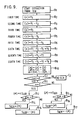
- Fig. 9 is a flow chart showing the operating sequence of a third embodiment of the present invention.
- the calculation algorithm to find the final GCR signal S GCR
- a decision step C1 and a result step C2 are inserted between step B10 and B11 of Fig. 3.
- step C1 it is therefore ascertained whether or not
- the present invention can of course be applied to a system wherein the final GCR signal (S GCR ) is obtained with a reduced noise signal by repeated performance of the calculation between the 8 fields.
Landscapes
- Engineering & Computer Science (AREA)
- Multimedia (AREA)
- Signal Processing (AREA)
- Picture Signal Circuits (AREA)
Applications Claiming Priority (2)
| Application Number | Priority Date | Filing Date | Title |
|---|---|---|---|
| JP250458/89 | 1989-09-28 | ||
| JP1250458A JP2835098B2 (ja) | 1989-09-28 | 1989-09-28 | ゴースト除去装置 |
Publications (2)
| Publication Number | Publication Date |
|---|---|
| EP0420688A2 true EP0420688A2 (de) | 1991-04-03 |
| EP0420688A3 EP0420688A3 (en) | 1991-11-27 |
Family
ID=17208178
Family Applications (1)
| Application Number | Title | Priority Date | Filing Date |
|---|---|---|---|
| EP19900310677 Withdrawn EP0420688A3 (en) | 1989-09-28 | 1990-09-28 | Ghost cancelling system and control method thereof |
Country Status (4)
| Country | Link |
|---|---|
| US (1) | US5130799A (de) |
| EP (1) | EP0420688A3 (de) |
| JP (1) | JP2835098B2 (de) |
| KR (1) | KR930001445B1 (de) |
Cited By (1)
| Publication number | Priority date | Publication date | Assignee | Title |
|---|---|---|---|---|
| EP0600740A3 (en) * | 1992-12-02 | 1994-07-20 | Samsung Electronics Co Ltd | Video signal processing for ghost cancellation. |
Families Citing this family (5)
| Publication number | Priority date | Publication date | Assignee | Title |
|---|---|---|---|---|
| JP2677035B2 (ja) * | 1991-03-14 | 1997-11-17 | 日本ビクター株式会社 | ゴースト除去装置 |
| KR0141579B1 (ko) * | 1991-12-11 | 1998-06-15 | 강진구 | 고스트제거장치 및 방법 |
| KR0126907B1 (ko) * | 1992-12-29 | 1997-12-29 | 윤종용 | 적응적 신호레벨조절기능을 구비한 고스트제거장치 |
| US6128337A (en) * | 1997-05-29 | 2000-10-03 | Trimble Navigation Limited | Multipath signal discrimination |
| US6760371B1 (en) * | 2000-03-22 | 2004-07-06 | The Boeing Company | Method and apparatus implementation of a zero forcing equalizer |
Family Cites Families (10)
| Publication number | Priority date | Publication date | Assignee | Title |
|---|---|---|---|---|
| US4335396A (en) * | 1980-11-13 | 1982-06-15 | Matsushita Electric Corporation | Automatic equalization system for television receiver |
| JPS59211315A (ja) * | 1983-05-17 | 1984-11-30 | Toshiba Corp | 自動等化器におけるタツプ利得修正方法 |
| JPS59211313A (ja) * | 1983-05-17 | 1984-11-30 | Toshiba Corp | 自動等化器 |
| JPS60199275A (ja) * | 1984-03-24 | 1985-10-08 | Toshiba Corp | ゴ−スト消去装置 |
| JPS60250782A (ja) * | 1984-05-28 | 1985-12-11 | Toshiba Corp | ゴ−スト消去装置 |
| JP2614633B2 (ja) * | 1988-03-11 | 1997-05-28 | 日本電気ホームエレクトロニクス株式会社 | ゴースト除去装置 |
| MY103982A (en) * | 1988-03-22 | 1993-10-30 | Nippon Denki Home Electronics | Ghost canceling apparatus. |
| JP2594639B2 (ja) * | 1989-03-23 | 1997-03-26 | 株式会社日立製作所 | テレビジョン映像受信信号波形歪み検出方法並びにそれに使用するテレビジョン映像信号送信装置および受信装置 |
| JP2619524B2 (ja) * | 1989-03-27 | 1997-06-11 | 日本電気ホームエレクトロニクス株式会社 | ゴースト検出用基準信号の抽出回路 |
| JP2904502B2 (ja) * | 1989-04-20 | 1999-06-14 | 株式会社リコー | ファクシミリ装置の記録出力方式 |
-
1989
- 1989-09-28 JP JP1250458A patent/JP2835098B2/ja not_active Expired - Lifetime
-
1990
- 1990-09-28 US US07/589,506 patent/US5130799A/en not_active Expired - Lifetime
- 1990-09-28 EP EP19900310677 patent/EP0420688A3/en not_active Withdrawn
- 1990-09-28 KR KR1019900015431A patent/KR930001445B1/ko not_active Expired - Fee Related
Cited By (2)
| Publication number | Priority date | Publication date | Assignee | Title |
|---|---|---|---|---|
| EP0600740A3 (en) * | 1992-12-02 | 1994-07-20 | Samsung Electronics Co Ltd | Video signal processing for ghost cancellation. |
| US5600380A (en) * | 1992-12-02 | 1997-02-04 | Samsung Electronics Co., Ltd. | Ghost-cancelation reference signal acquisition circuitry, as for TV receiver or video recorder |
Also Published As
| Publication number | Publication date |
|---|---|
| JPH03114366A (ja) | 1991-05-15 |
| JP2835098B2 (ja) | 1998-12-14 |
| KR910007351A (ko) | 1991-04-30 |
| KR930001445B1 (ko) | 1993-02-27 |
| US5130799A (en) | 1992-07-14 |
| EP0420688A3 (en) | 1991-11-27 |
Similar Documents
| Publication | Publication Date | Title |
|---|---|---|
| FI90607B (fi) | Digitaalinen skaalauspiiri katkaisupoikkeaman kompensoimiseksi | |
| EP0125649B1 (de) | Automatischer Entzerrer | |
| EP0969658B1 (de) | Signalverarbeitungsschaltung zur Rauschunterdrückung und Anzeigegerät | |
| US7738042B2 (en) | Noise reduction device for a video signal and noise reduction method for a video signal | |
| KR0143389B1 (ko) | 윤곽보정장치 | |
| KR930003567B1 (ko) | 고스트 제거장치 및 그 제거 방법 | |
| EP0420688A2 (de) | System zum Auslöschung von Geisterbildern und Steuerverfahren dafür | |
| EP0107463B1 (de) | Digitales Fernsehsystem mit Fehlerkorrektur | |
| US6188788B1 (en) | Automatic color saturation control in video decoder using recursive algorithm | |
| WO2009069366A1 (en) | Noise reducing circuit, noise reducing method, and video apparatus | |
| JPS59224985A (ja) | ゴ−スト除去装置 | |
| JP2548991B2 (ja) | 波形歪除去装置 | |
| JPH0523543B2 (de) | ||
| JP3077163B2 (ja) | 波形歪み成分の除去回路 | |
| JPS627750B2 (de) | ||
| JP2862700B2 (ja) | 動き検出装置 | |
| JPH11239361A (ja) | 信号処理装置 | |
| JPH06303462A (ja) | 画質補正装置 | |
| JPH02141068A (ja) | ディジタル・ノイズリデューサ | |
| JPH0660540A (ja) | 信号補正回路 | |
| JPS6386967A (ja) | ゴ−スト除去装置 | |
| JPH0556344A (ja) | ビデオカメラのγ補正回路 | |
| JPH07297715A (ja) | A/d変換ノイズ抑制回路 | |
| JPH0720257B2 (ja) | 輝度信号・色信号分離回路 | |
| JPH04180472A (ja) | ゴースト除去装置 |
Legal Events
| Date | Code | Title | Description |
|---|---|---|---|
| PUAI | Public reference made under article 153(3) epc to a published international application that has entered the european phase |
Free format text: ORIGINAL CODE: 0009012 |
|
| 17P | Request for examination filed |
Effective date: 19901019 |
|
| AK | Designated contracting states |
Kind code of ref document: A2 Designated state(s): DE FR GB NL |
|
| PUAL | Search report despatched |
Free format text: ORIGINAL CODE: 0009013 |
|
| AK | Designated contracting states |
Kind code of ref document: A3 Designated state(s): DE FR GB NL |
|
| STAA | Information on the status of an ep patent application or granted ep patent |
Free format text: STATUS: THE APPLICATION HAS BEEN WITHDRAWN |
|
| 18W | Application withdrawn |
Withdrawal date: 19920609 |