EP0422901A1 - MOS-Feldeffekttransistor und Verfahren zur Herstellung - Google Patents
MOS-Feldeffekttransistor und Verfahren zur Herstellung Download PDFInfo
- Publication number
- EP0422901A1 EP0422901A1 EP90311059A EP90311059A EP0422901A1 EP 0422901 A1 EP0422901 A1 EP 0422901A1 EP 90311059 A EP90311059 A EP 90311059A EP 90311059 A EP90311059 A EP 90311059A EP 0422901 A1 EP0422901 A1 EP 0422901A1
- Authority
- EP
- European Patent Office
- Prior art keywords
- insulation layer
- region
- field effect
- effect transistor
- mos field
- Prior art date
- Legal status (The legal status is an assumption and is not a legal conclusion. Google has not performed a legal analysis and makes no representation as to the accuracy of the status listed.)
- Granted
Links
- 230000005669 field effect Effects 0.000 title claims abstract description 23
- 238000000034 method Methods 0.000 title claims description 11
- 238000004519 manufacturing process Methods 0.000 title claims description 10
- 238000009413 insulation Methods 0.000 claims abstract description 94
- BPUBBGLMJRNUCC-UHFFFAOYSA-N oxygen(2-);tantalum(5+) Chemical compound [O-2].[O-2].[O-2].[O-2].[O-2].[Ta+5].[Ta+5] BPUBBGLMJRNUCC-UHFFFAOYSA-N 0.000 claims abstract description 15
- 229910001936 tantalum oxide Inorganic materials 0.000 claims abstract description 13
- 239000000969 carrier Substances 0.000 claims abstract description 12
- 239000000758 substrate Substances 0.000 claims description 32
- VYPSYNLAJGMNEJ-UHFFFAOYSA-N Silicium dioxide Chemical compound O=[Si]=O VYPSYNLAJGMNEJ-UHFFFAOYSA-N 0.000 claims description 28
- 229910052814 silicon oxide Inorganic materials 0.000 claims description 28
- 239000012535 impurity Substances 0.000 claims description 26
- 239000004065 semiconductor Substances 0.000 claims description 15
- 238000005229 chemical vapour deposition Methods 0.000 claims description 6
- 238000000151 deposition Methods 0.000 claims description 4
- 238000005530 etching Methods 0.000 claims description 2
- 239000010410 layer Substances 0.000 description 32
- 229910052581 Si3N4 Inorganic materials 0.000 description 7
- HQVNEWCFYHHQES-UHFFFAOYSA-N silicon nitride Chemical compound N12[Si]34N5[Si]62N3[Si]51N64 HQVNEWCFYHHQES-UHFFFAOYSA-N 0.000 description 7
- 230000005684 electric field Effects 0.000 description 6
- 238000004088 simulation Methods 0.000 description 5
- XUIMIQQOPSSXEZ-UHFFFAOYSA-N Silicon Chemical compound [Si] XUIMIQQOPSSXEZ-UHFFFAOYSA-N 0.000 description 4
- 238000005468 ion implantation Methods 0.000 description 4
- 229910021420 polycrystalline silicon Inorganic materials 0.000 description 4
- 229920005591 polysilicon Polymers 0.000 description 4
- 229910052710 silicon Inorganic materials 0.000 description 4
- 239000010703 silicon Substances 0.000 description 4
- 229910052785 arsenic Inorganic materials 0.000 description 3
- RQNWIZPPADIBDY-UHFFFAOYSA-N arsenic atom Chemical compound [As] RQNWIZPPADIBDY-UHFFFAOYSA-N 0.000 description 3
- BHEPBYXIRTUNPN-UHFFFAOYSA-N hydridophosphorus(.) (triplet) Chemical compound [PH] BHEPBYXIRTUNPN-UHFFFAOYSA-N 0.000 description 3
- 239000000463 material Substances 0.000 description 3
- 230000001133 acceleration Effects 0.000 description 2
- 238000012986 modification Methods 0.000 description 2
- 230000004048 modification Effects 0.000 description 2
- 230000003071 parasitic effect Effects 0.000 description 2
- 238000001020 plasma etching Methods 0.000 description 2
- 230000015572 biosynthetic process Effects 0.000 description 1
- 239000004020 conductor Substances 0.000 description 1
- 230000000875 corresponding effect Effects 0.000 description 1
- 230000003247 decreasing effect Effects 0.000 description 1
- 230000001419 dependent effect Effects 0.000 description 1
- 239000003989 dielectric material Substances 0.000 description 1
- 230000000694 effects Effects 0.000 description 1
- 238000005755 formation reaction Methods 0.000 description 1
- 238000007254 oxidation reaction Methods 0.000 description 1
- QHGVXILFMXYDRS-UHFFFAOYSA-N pyraclofos Chemical compound C1=C(OP(=O)(OCC)SCCC)C=NN1C1=CC=C(Cl)C=C1 QHGVXILFMXYDRS-UHFFFAOYSA-N 0.000 description 1
Images


Classifications
-
- H—ELECTRICITY
- H10—SEMICONDUCTOR DEVICES; ELECTRIC SOLID-STATE DEVICES NOT OTHERWISE PROVIDED FOR
- H10D—INORGANIC ELECTRIC SEMICONDUCTOR DEVICES
- H10D64/00—Electrodes of devices having potential barriers
- H10D64/01—Manufacture or treatment
- H10D64/021—Manufacture or treatment using multiple gate spacer layers, e.g. bilayered sidewall spacers
-
- H—ELECTRICITY
- H10—SEMICONDUCTOR DEVICES; ELECTRIC SOLID-STATE DEVICES NOT OTHERWISE PROVIDED FOR
- H10D—INORGANIC ELECTRIC SEMICONDUCTOR DEVICES
- H10D30/00—Field-effect transistors [FET]
- H10D30/01—Manufacture or treatment
- H10D30/021—Manufacture or treatment of FETs having insulated gates [IGFET]
- H10D30/0223—Manufacture or treatment of FETs having insulated gates [IGFET] having source and drain regions or source and drain extensions self-aligned to sides of the gate
- H10D30/0227—Manufacture or treatment of FETs having insulated gates [IGFET] having source and drain regions or source and drain extensions self-aligned to sides of the gate having both lightly-doped source and drain extensions and source and drain regions self-aligned to the sides of the gate, e.g. lightly-doped drain [LDD] MOSFET or double-diffused drain [DDD] MOSFET
-
- H—ELECTRICITY
- H10—SEMICONDUCTOR DEVICES; ELECTRIC SOLID-STATE DEVICES NOT OTHERWISE PROVIDED FOR
- H10D—INORGANIC ELECTRIC SEMICONDUCTOR DEVICES
- H10D30/00—Field-effect transistors [FET]
- H10D30/60—Insulated-gate field-effect transistors [IGFET]
-
- Y—GENERAL TAGGING OF NEW TECHNOLOGICAL DEVELOPMENTS; GENERAL TAGGING OF CROSS-SECTIONAL TECHNOLOGIES SPANNING OVER SEVERAL SECTIONS OF THE IPC; TECHNICAL SUBJECTS COVERED BY FORMER USPC CROSS-REFERENCE ART COLLECTIONS [XRACs] AND DIGESTS
- Y10—TECHNICAL SUBJECTS COVERED BY FORMER USPC
- Y10S—TECHNICAL SUBJECTS COVERED BY FORMER USPC CROSS-REFERENCE ART COLLECTIONS [XRACs] AND DIGESTS
- Y10S257/00—Active solid-state devices, e.g. transistors, solid-state diodes
- Y10S257/90—MOSFET type gate sidewall insulating spacer
Definitions
- the present invention relates to an MOS field effect transistor having an LDD structure.
- a transistor having a lightly doped drain structure (hereinafter referred to as an "LDD transistor") is well known in the art.
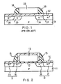
- Fig. 1 is a sectional view showing the element structure of a conventional LDD transistor.
- a gate electrode 33 is formed on a p-type silicon semiconductor substrate 31, such that a silicon oxide film 32 having a thickness of e.g. 150 ⁇ is interposed therebetween.
- Two n ⁇ -type regions 34 and 35 each having a comparatively low impurity concentration and two n+-type regions 37 and 38 each having a comparatively high impurity concentration, are formed inside the substrate 31.
- the n ⁇ -type regions 34 and 35 are formed by ion implantation of n-type impurities by using the gate electrode 33 as a mask, while the n ⁇ -type regions 37 and 38 are formed by ion implantation of n-type impurities by using a CVD oxide film 36 located on the side wall of the gate electrode 33 as a mask.
- the n ⁇ -type region 34 and the n+-type region 37 jointly constitute a drain region, while the n ⁇ -type region 35 and n+-type region 38 jointly constitute a source region.
- the low-impurity concentration n ⁇ -type region 34 is located between the source and drain regions. Since, therefore, a depletion layer is constantly formed inside the n ⁇ -type region 34, the current-driving ability of the LDD transistor is not as good as that of an ordinary-structure MOS transistor. Thus, it is impossible for the LDD transistor to produce a drain current in large quantities.
- the first object of the present invention is to provide an MOS field effect transistor which enables miniaturization of an element to the same degree as in the prior art, has improved ability to drive current, and is easy to manufacture.
- the second object of the present invention is to provide a method for manufacturing such an MOS field effect transistor.
- the present invention provides an MOS field effect transistor which comprises: a semiconductor substrate of a first conductivity type; a source region and a drain region, both of a second conductivity type, which are formed inside the substrate and are isolated from each other by a predetermined distance; a first insulation layer formed on the substrate and located between the source region and the drain region; a gate electrode conductive layer formed on the first insulation layer; a pair of second insulation layers formed on opposing side walls of the gate electrode conductive layer, respectively, and having a dielectric constant larger than that of the first insulation layer; and a third insulation layer formed between the second insulation layers and the source and drain regions, the third insulation layer having a thickness which is greater than that of the first insulation layer and which is greater than the length of a mean free path of hot carriers generated in the vicinity of the drain region.
- the present invention provides an MOS field effect transistor-manufacturing method which comprises the steps of: forming a first insulation layer on a semiconductor substrate of a first conductivity type; depositing a conductive layer on the first insulation layer; selectively removing a laminated structure made up of the conductive layer and the first insulation layer, such that the laminated structure has a predetermined shape; forming a second insulation layer, which is thicker than the first insulation layer, over the resultant semiconductor structure such that the second insulation layer is formed at least on the laminated structure; forming a low-concentration impurity region in the substrate by introducing impurities of a second conductivity into the substrate at a low doping rate, with the laminated structure used as a mask; depositing a third insulation layer, which has a dielectric constant larger than that of the first insulation layer, over the semiconductor structure by chemical vapor deposition; removing the third insulation layer by anisotropic etching such that the third insulation layer is left on the opposing side walls
- a silicon oxide film 12 having a thickness of e.g. 60 ⁇ is formed on part of the surface of a p-type silicon semiconductor substrate 11.
- a polysilicon gate electrode 13 is formed on the silicon oxide film 12.
- the gate electrode 13 has reduced resistance since a conductive material, such as impurities, is introduced into it.
- a silicon oxide film 14 having a thickness of e.g. 90 ⁇ is formed on the surfaces of both the substrate 11 and the gate electrode 13.
- an insulation film 15 is formed, with the silicon oxide film 14 interposed.
- the insulation film 15 is formed of a material whose dielectric constant is at least larger than the dielectric constant of silicon oxide.
- the insulation film 15 is formed of tantalum oxide (Ta2O5).
- Ta2O5 tantalum oxide
- the insulation film 15 has a larger amount of band gap energy than that of the silicon oxide 14.
- the band gap energy of the silicon oxide film 14 is approximately 9 eV.
- a drain region D and a source region S are formed in a surface region of the substrate 11.
- the drain region D is made up of: an n ⁇ region 16 which contains a comparatively low concentration of phosphorous (P) as n-type impurities; and an n+-type region 17 which is adjacent to the n ⁇ -type region 16 and contains a comparatively high concentration of arsenic (As) as n-type impurities.
- the source region S is made up of: an n ⁇ region 18 which contains a comparatively low concentration of phosphorous (P); and an n+-type region 19 which is adjacent to the n ⁇ -type region 18 and contains a comparatively high concentration of arsenic (As).
- the n+-type region 17 of the drain region and the n+-type region 19 of the source region S are located on the laterally outer sides than the side walls of the gate electrode 13.
- the insulation film 15 which is formed of a material having a large dielectric constant is located on the side walls of the gate electrode 13.
- the gate electrode 13 is applied with a predetermined voltage of positive polarity, an intense electric field is generated from the side faces of the gate electrode toward the substrate 11.
- Fig. 3 To examine the characteristics of an LDD transistor having the structure illustrated in Fig. 2, two-dimensional device simulation was carried out. The results of this simulation are shown in Fig. 3.
- the origin corresponds to a point located in the boundary between the gate electrode 13 and the drain region D
- the abscissa represents the horizontal distance X ( ⁇ m) by which a given point is located away from the point of the boundary
- the ordinate represents the field intensity (MV/cm) measured at the given point.
- the gate length was 0.5 ⁇ m
- the gate voltage was 3V
- the drain voltage was 6V.
- the data indicated by the solid lines corresponds to a device embodying the present invention, wherein the insulation films 15 on the side walls of the gate electrode 13 are formed of tantalum oxide whose dielectric constant ⁇ is 30.
- the data indicated by the dot-dash broken lines corresponds to a device wherein the insulation films 15 are formed of silicon nitride (Si3N4) whose dielectric constant ⁇ is 7.5.
- the data indicated by the long-stroke broken lines corresponds to a device wherein the insulation films 15 are formed of silicon oxide (SiO2) whose dielectric constant ⁇ is 3.9.
- the data indicated by the short-stroke broken lines corresponds to a device wherein no insulation film is formed on the side walls of the gate electrode 13 is formed of silicon nitride (Si3N4), that is, a vacuum state (dielectric constant ⁇ : 1.0) is assumed in this case.
- the intensity of the drain electric field is considerably reduced in the neighborhood of the gate electrode, as is seen from the portion circled in the Fig. 3 graph.
- This phenomenon is attributable to the fact that the insulation film 15 (which has a large dielectric constant) reduces the maximum electric field acting in the plane of the silicon substrate surface and narrows the range of the maximum electric field. Since the intensity of the drain electric field is considerably reduced in the neighborhood of the gate electrode, the impact ionization is suppressed in the vicinity of the drain, even when an ON current is made to flow between the source and drain regions by providing a predetermined potential difference therebetween. Therefore, the generation of hot carriers is suppressed, so that high reliability of the device is attained.
- the 90 ⁇ -thick silicon oxide film 14 is located between the drain region D and the insulation film 15.
- the thickness of the silicon oxide film 14 is far greater than the length (length: about 20 ⁇ ) of the mean free path of hot carriers which may be generated in the vicinity of the drain region as a result of the impact ionization.
- the band gap energy of the silicon oxide film 14 is as high as 9 eV. Therefore, even if hot carriers are generated in the vicinity of the drain, the hot carriers hardly pass through the silicon oxide film 14 or reach the insulation film 15. As a result, very few hot carriers are trapped in the interior of the insulation film 15 or in the interface between the insulation films 14 and 15. Consequently, the reliability of the device is improved.
- the embodiment device is of an LDD structure.
- an element can be miniaturized to substantially the same degree as in the prior art.
- the data indicated by the solid lines corresponds to a device wherein the insulation film 15 is formed of tantalum oxide whose dielectric constant ⁇ is 30, the data indicated by the dot-dash broken lines corresponds to a device wherein the insulation film 15 is formed of silicon nitride (Si3N4) whose dielectric constant ⁇ is 7.5, the data indicated by the long-stroke broken lines corresponds to a device wherein the insulation film 15 is formed of silicon oxide (SiO2) whose dielectric constant ⁇ is 3.9, and the data indicated by the short-stroke broken lines corresponds to a device wherein no insulation film is formed and a vacuum state (dielectric constant ⁇ : 1.0) is assumed.
- the electron density in the n ⁇ -type layer 18 of the source region S increases with an increase in the intensity of the electric field generated from the side of the gate electrode.
- the electron density in the source region S is dependent on the dielectric constant ⁇ of the insulation film 15.
- the insulation film 15 is formed of tantalum oxide (whose dielectric constant ⁇ is as large as 30)
- the range of the depletion layer inside the n ⁇ -type region 17 is narrow. For this reason, the parasitic resistance of the n ⁇ -type region of the embodiment device is decreased, thus increasing the drain current.
- the MOS transistor of the embodiment has high ability to drive current.
- the insulation film 15 located on the side walls of the gate electrode 13 is formed of tantalum oxide having a large dielectric constant ⁇ , and the silicon oxide film 14, whose thickness is far greater than the length of the mean free path of hot carriers, is located between the insulation film 15 and the drain region D.
- the embodiment device is very reliable and has high current-driving ability.
- Figs. 5A-5F the same reference numerals as in Fig. 2 are used to denote the structural elements corresponding to those shown in Fig. 2.
- the surfapce of a p-type silicon semiconductor substrate 11 is thermally oxidized, so as to form a 60 ⁇ -thick silicon oxide film 12 on the entire surface of the substrate.
- a 0.2 ⁇ m-thick polysilicon layer is deposited over the resultant semiconductor structure by chemical vapor deposition (CVD).
- the silicon oxide layer 12 and the polysilicon layer jointly constitute a laminated film.
- this laminated film is selectively removed, to thereby form a gate electrode 13 having a predetermined shape, as is shown in Fig. 5B.
- n-type or p-type impurities are introduced, so that the resultant gate electrode 13 has reduced resistance.
- the impurities may be introduced after the gate electrode 13 is patterned into the predetermined shape.
- a 90 ⁇ -thick silicon oxide film 14 is formed on the surface of the gate electrode 13 and that of the substrate 11 by thermal oxidization. Subsequently, by use of the gate electrode 13 as a mask, phosphorous (P) is ion-implanted into the substrate 11 by application of an acceleration voltage of 40 KeV and in a dose of 5 ⁇ 1013 atoms/cm2, to thereby form n ⁇ -type regions 15 and 17 having a comparatively low impurity concentration.
- P phosphorous
- a tantalum oxide (Ta2O5) film 20 having a thickness of 0.15 ⁇ m is deposited by CVD over the semiconductor structure, including the surface of the gate electrode 13.
- the tantalum oxide film 20, thus deposited is removed by reactive ion etching (RIE), such that the tantalum oxide film 20 is left only on a pair of opposing side walls of the gate electrode 13, as is shown in Fig. 5E.
- the tantalum oxide film 20 left on the opposing side walls constitutes an insulation film 15.
- the present invention is not limited to the embodiment mentioned above, and may be modified in various manners without departing from the spirit and scope of the invention.
- the above embodiment was described, referring to the case where the insulation film 15 was formed of tantalum oxide.
- the silicon oxide film 12 constitutes a gate insulation film, but this gate insulation film may be constituted by a laminated film made up of a silicon oxide film and a silicon nitride film.
- the gate insulation film may be either a so-called ONO film, a oxy-nytride film, or the like.
- the low-impurity concentration n ⁇ -type regions 15 and 17 were described, with reference to Fig. 5C, as being formed by ion implantation after the formation of the silicon oxide film 14.
- the step of forming the n ⁇ -type regions 15 and 17 may be carried out first, being followed by the step of forming the silicon oxide film 14 over the semiconductor structure.
- the present invention can provide an MOS field effect transistor which enables miniaturization of an element to the same degree as in the prior art, has improved ability to drive current, and is easy to manufacture.
- the present invention can also provide a method for manufacturing such an MOS field effect transistor.
Landscapes
- Insulated Gate Type Field-Effect Transistor (AREA)
- Metal-Oxide And Bipolar Metal-Oxide Semiconductor Integrated Circuits (AREA)
Applications Claiming Priority (2)
| Application Number | Priority Date | Filing Date | Title |
|---|---|---|---|
| JP26205989 | 1989-10-09 | ||
| JP262059/89 | 1989-10-09 |
Publications (2)
| Publication Number | Publication Date |
|---|---|
| EP0422901A1 true EP0422901A1 (de) | 1991-04-17 |
| EP0422901B1 EP0422901B1 (de) | 1995-09-13 |
Family
ID=17370460
Family Applications (1)
| Application Number | Title | Priority Date | Filing Date |
|---|---|---|---|
| EP90311059A Expired - Lifetime EP0422901B1 (de) | 1989-10-09 | 1990-10-09 | MOS-Feldeffekttransistor und Verfahren zur Herstellung |
Country Status (5)
| Country | Link |
|---|---|
| US (1) | US5698883A (de) |
| EP (1) | EP0422901B1 (de) |
| JP (1) | JPH0834313B2 (de) |
| KR (1) | KR910008857A (de) |
| DE (1) | DE69022346T2 (de) |
Cited By (2)
| Publication number | Priority date | Publication date | Assignee | Title |
|---|---|---|---|---|
| EP0490535A3 (de) * | 1990-12-07 | 1994-04-06 | American Telephone & Telegraph | |
| WO1994019830A1 (en) * | 1993-02-23 | 1994-09-01 | Thunderbird Technologies, Inc. | High saturation current, low leakage current fermi threshold field effect transistor |
Families Citing this family (14)
| Publication number | Priority date | Publication date | Assignee | Title |
|---|---|---|---|---|
| JPH0629524A (ja) * | 1992-04-14 | 1994-02-04 | Toshiba Corp | 半導体装置の製造方法 |
| JP3587537B2 (ja) * | 1992-12-09 | 2004-11-10 | 株式会社半導体エネルギー研究所 | 半導体装置 |
| JP3256084B2 (ja) * | 1994-05-26 | 2002-02-12 | 株式会社半導体エネルギー研究所 | 半導体集積回路およびその作製方法 |
| US5714413A (en) * | 1995-12-11 | 1998-02-03 | Intel Corporation | Method of making a transistor having a deposited dual-layer spacer structure |
| US5952720A (en) * | 1996-05-06 | 1999-09-14 | United Microelectronics Corp. | Buried contact structure |
| US5672525A (en) * | 1996-05-23 | 1997-09-30 | Chartered Semiconductor Manufacturing Pte Ltd. | Polysilicon gate reoxidation in a gas mixture of oxygen and nitrogen trifluoride gas by rapid thermal processing to improve hot carrier immunity |
| JPH10178172A (ja) | 1996-12-17 | 1998-06-30 | Toshiba Corp | 半導体装置及びその製造方法 |
| US6251763B1 (en) * | 1997-06-30 | 2001-06-26 | Kabushiki Kaisha Toshiba | Semiconductor device and method for manufacturing same |
| US6271563B1 (en) * | 1998-07-27 | 2001-08-07 | Advanced Micro Devices, Inc. | MOS transistor with high-K spacer designed for ultra-large-scale integration |
| KR100338099B1 (ko) * | 1999-06-29 | 2002-05-24 | 박종섭 | 반도체 소자의 제조 방법 |
| JP2002212537A (ja) * | 2001-01-24 | 2002-07-31 | Sony Chem Corp | 接着剤及び電気装置 |
| US6583016B1 (en) * | 2002-03-26 | 2003-06-24 | Advanced Micro Devices, Inc. | Doped spacer liner for improved transistor performance |
| US20050274994A1 (en) * | 2004-06-14 | 2005-12-15 | Rhodes Howard E | High dielectric constant spacer for imagers |
| US10515976B2 (en) * | 2018-02-01 | 2019-12-24 | United Microelectronics Corp. | Semiconductor device and method for fabricating the same |
Citations (1)
| Publication number | Priority date | Publication date | Assignee | Title |
|---|---|---|---|---|
| EP0218408A2 (de) * | 1985-09-25 | 1987-04-15 | Hewlett-Packard Company | Verfahren zum Herstellen einer schwach dotierten Drainstruktur (LLD) in integrierten Schaltungen |
Family Cites Families (18)
| Publication number | Priority date | Publication date | Assignee | Title |
|---|---|---|---|---|
| US4638347A (en) * | 1982-12-07 | 1987-01-20 | International Business Machines Corporation | Gate electrode sidewall isolation spacer for field effect transistors |
| JPS59124768A (ja) * | 1982-12-29 | 1984-07-18 | Fujitsu Ltd | 不揮発性半導体記憶装置の製造方法 |
| JPS59205759A (ja) * | 1983-04-01 | 1984-11-21 | Hitachi Ltd | Mis型電界効果トランジスタ |
| JPS59231864A (ja) * | 1983-06-15 | 1984-12-26 | Hitachi Ltd | 半導体装置 |
| JPS60158669A (ja) * | 1984-01-28 | 1985-08-20 | Sharp Corp | 半導体装置 |
| DE3581797D1 (de) * | 1984-12-27 | 1991-03-28 | Toshiba Kawasaki Kk | Misfet mit niedrigdotiertem drain und verfahren zu seiner herstellung. |
| JPH0650778B2 (ja) * | 1985-08-20 | 1994-06-29 | 松下電器産業株式会社 | 薄膜トランジスタおよびその製造方法 |
| JPS62156873A (ja) * | 1985-12-28 | 1987-07-11 | Toshiba Corp | 半導体装置 |
| JPS62160770A (ja) * | 1986-01-09 | 1987-07-16 | Toshiba Corp | 絶縁ゲート型電界効果トランジスタおよびその製造方法 |
| JPS62274665A (ja) * | 1986-05-22 | 1987-11-28 | Nec Corp | 半導体装置の製造方法 |
| US4894694A (en) * | 1986-10-31 | 1990-01-16 | Hewlett-Packard Company | MOSFET structure and method for making same |
| JPS63140580A (ja) * | 1986-12-02 | 1988-06-13 | Matsushita Electric Ind Co Ltd | 薄膜トランジスタ |
| JPH0666328B2 (ja) * | 1987-05-28 | 1994-08-24 | 松下電器産業株式会社 | Mos型半導体装置 |
| JPS63316476A (ja) * | 1987-06-18 | 1988-12-23 | Seiko Instr & Electronics Ltd | 半導体装置およびその製造方法 |
| JPS64761A (en) * | 1987-06-23 | 1989-01-05 | Seiko Epson Corp | Semiconductor device |
| JPH01125977A (ja) * | 1987-11-11 | 1989-05-18 | Toshiba Corp | Mos型半導体装置 |
| JP2667857B2 (ja) * | 1988-02-12 | 1997-10-27 | 株式会社日立製作所 | 半導体装置およびその製造方法 |
| JPH01264265A (ja) * | 1988-04-15 | 1989-10-20 | Hitachi Ltd | 半導体装置およびその製造方法 |
-
1990
- 1990-08-15 JP JP2215484A patent/JPH0834313B2/ja not_active Expired - Lifetime
- 1990-10-08 KR KR1019900015933A patent/KR910008857A/ko not_active Withdrawn
- 1990-10-09 EP EP90311059A patent/EP0422901B1/de not_active Expired - Lifetime
- 1990-10-09 DE DE69022346T patent/DE69022346T2/de not_active Expired - Fee Related
-
1996
- 1996-05-28 US US08/654,754 patent/US5698883A/en not_active Expired - Fee Related
Patent Citations (1)
| Publication number | Priority date | Publication date | Assignee | Title |
|---|---|---|---|---|
| EP0218408A2 (de) * | 1985-09-25 | 1987-04-15 | Hewlett-Packard Company | Verfahren zum Herstellen einer schwach dotierten Drainstruktur (LLD) in integrierten Schaltungen |
Non-Patent Citations (3)
| Title |
|---|
| INTERNATIONAL ELECTRON DEVICES MEETING 1988 . SAN FRANCISCO, CA .DECEMBER 11-14, 1988 pages 234 - 237; TOMOHISA MIZUNO et al: "Si3N4/SiO2 Spacer Induced High Reliability in LDDMOSFET and Its Simple Degradation Model" * |
| PATENT ABSTRACTS OF JAPAN vol. 10, no. 186 (E-416)(2242) 28 June 1986, & JP-A-61 32576 (HITACHI LTD) 15 February 1986, * |
| PATENT ABSTRACTS OF JAPAN vol. 10, no. 376 (E-464)(2433) 13 December 1986, & JP-A-61 168264 (NEC CORP) 29 July 1986, * |
Cited By (2)
| Publication number | Priority date | Publication date | Assignee | Title |
|---|---|---|---|---|
| EP0490535A3 (de) * | 1990-12-07 | 1994-04-06 | American Telephone & Telegraph | |
| WO1994019830A1 (en) * | 1993-02-23 | 1994-09-01 | Thunderbird Technologies, Inc. | High saturation current, low leakage current fermi threshold field effect transistor |
Also Published As
| Publication number | Publication date |
|---|---|
| KR910008857A (ko) | 1991-05-31 |
| DE69022346D1 (de) | 1995-10-19 |
| JPH0834313B2 (ja) | 1996-03-29 |
| US5698883A (en) | 1997-12-16 |
| DE69022346T2 (de) | 1996-04-04 |
| JPH03204941A (ja) | 1991-09-06 |
| EP0422901B1 (de) | 1995-09-13 |
Similar Documents
| Publication | Publication Date | Title |
|---|---|---|
| US6426279B1 (en) | Epitaxial delta doping for retrograde channel profile | |
| US5583067A (en) | Inverse T-gate semiconductor device with self-aligned punchthrough stops and method of fabrication | |
| EP0422901A1 (de) | MOS-Feldeffekttransistor und Verfahren zur Herstellung | |
| US4597827A (en) | Method of making MIS field effect transistor having a lightly-doped region | |
| US4722909A (en) | Removable sidewall spacer for lightly doped drain formation using two mask levels | |
| KR100392901B1 (ko) | 비대칭약간도프된드레인(lcd)mos소자의제조방법 | |
| US4319395A (en) | Method of making self-aligned device | |
| EP0164449B1 (de) | Verfahren zum Herstellen einer integrierten Halbleiterschaltkreisanordnung mit einem MISFET | |
| EP0387722B1 (de) | MOSFET-Transistor mit nicht-gleichmässiger Schwellspannung im Kanalbereich | |
| EP0150597A1 (de) | Verfahren zum Herstellen eines Halbleiterspeicherelementes mit grabenförmigem Speicherkondensator | |
| EP0266768B1 (de) | Herstellungsverfahren zur Ausbildung eines MOS-Transistors durch Selbstausrichtung der Source/Drain-Gebiete | |
| US6388298B1 (en) | Detached drain MOSFET | |
| EP0603102A2 (de) | Wiedertemperatur-MOSFET-Source/Drain-Struktur mit ultrakurzem Kanal | |
| JPH01205470A (ja) | 半導体装置およびその製造方法 | |
| US6077736A (en) | Method of fabricating a semiconductor device | |
| US6207482B1 (en) | Integration method for deep sub-micron dual gate transistor design | |
| EP0881670A2 (de) | Hilfsseitenwandabstandsstück für integrierte Schaltungstransistoren | |
| US6117739A (en) | Semiconductor device with layered doped regions and methods of manufacture | |
| US6025239A (en) | Method for fabricating an electrostatic discharge device | |
| JPH05102179A (ja) | 半導体装置及びその製造方法 | |
| US5612243A (en) | Polycide local interconnect method and structure | |
| Miyake et al. | Characteristics of buried-channel pMOS devices with shallow counter-doped layers fabricated using channel preamorphization | |
| EP0098737A2 (de) | Halbleiteranordnung | |
| JP2730535B2 (ja) | 半導体装置の製造方法 | |
| JPS63168050A (ja) | 半導体装置 |
Legal Events
| Date | Code | Title | Description |
|---|---|---|---|
| PUAI | Public reference made under article 153(3) epc to a published international application that has entered the european phase |
Free format text: ORIGINAL CODE: 0009012 |
|
| 17P | Request for examination filed |
Effective date: 19901101 |
|
| AK | Designated contracting states |
Kind code of ref document: A1 Designated state(s): DE FR GB |
|
| 17Q | First examination report despatched |
Effective date: 19930422 |
|
| GRAA | (expected) grant |
Free format text: ORIGINAL CODE: 0009210 |
|
| AK | Designated contracting states |
Kind code of ref document: B1 Designated state(s): DE FR GB |
|
| REF | Corresponds to: |
Ref document number: 69022346 Country of ref document: DE Date of ref document: 19951019 |
|
| ET | Fr: translation filed | ||
| PLBE | No opposition filed within time limit |
Free format text: ORIGINAL CODE: 0009261 |
|
| STAA | Information on the status of an ep patent application or granted ep patent |
Free format text: STATUS: NO OPPOSITION FILED WITHIN TIME LIMIT |
|
| 26N | No opposition filed | ||
| REG | Reference to a national code |
Ref country code: GB Ref legal event code: 746 Effective date: 19980910 |
|
| REG | Reference to a national code |
Ref country code: FR Ref legal event code: D6 |
|
| REG | Reference to a national code |
Ref country code: GB Ref legal event code: IF02 |
|
| PGFP | Annual fee paid to national office [announced via postgrant information from national office to epo] |
Ref country code: DE Payment date: 20071004 Year of fee payment: 18 |
|
| PGFP | Annual fee paid to national office [announced via postgrant information from national office to epo] |
Ref country code: FR Payment date: 20071009 Year of fee payment: 18 Ref country code: GB Payment date: 20071003 Year of fee payment: 18 |
|
| GBPC | Gb: european patent ceased through non-payment of renewal fee |
Effective date: 20081009 |
|
| REG | Reference to a national code |
Ref country code: FR Ref legal event code: ST Effective date: 20090630 |
|
| PG25 | Lapsed in a contracting state [announced via postgrant information from national office to epo] |
Ref country code: DE Free format text: LAPSE BECAUSE OF NON-PAYMENT OF DUE FEES Effective date: 20090501 |
|
| PG25 | Lapsed in a contracting state [announced via postgrant information from national office to epo] |
Ref country code: FR Free format text: LAPSE BECAUSE OF NON-PAYMENT OF DUE FEES Effective date: 20081031 |
|
| PG25 | Lapsed in a contracting state [announced via postgrant information from national office to epo] |
Ref country code: GB Free format text: LAPSE BECAUSE OF NON-PAYMENT OF DUE FEES Effective date: 20081009 |