EP0423451A2 - Spitzenstromdetektor - Google Patents
Spitzenstromdetektor Download PDFInfo
- Publication number
- EP0423451A2 EP0423451A2 EP90115285A EP90115285A EP0423451A2 EP 0423451 A2 EP0423451 A2 EP 0423451A2 EP 90115285 A EP90115285 A EP 90115285A EP 90115285 A EP90115285 A EP 90115285A EP 0423451 A2 EP0423451 A2 EP 0423451A2
- Authority
- EP
- European Patent Office
- Prior art keywords
- analog
- output
- input
- digital
- comparator
- Prior art date
- Legal status (The legal status is an assumption and is not a legal conclusion. Google has not performed a legal analysis and makes no representation as to the accuracy of the status listed.)
- Granted
Links
Images


Classifications
-
- G—PHYSICS
- G01—MEASURING; TESTING
- G01R—MEASURING ELECTRIC VARIABLES; MEASURING MAGNETIC VARIABLES
- G01R19/00—Arrangements for measuring currents or voltages or for indicating presence or sign thereof
- G01R19/04—Measuring peak values or amplitude or envelope of AC or of pulses
Definitions
- the invention disclosed broadly relates to testing circuits and more particularly relates to a testing circuit for measuring very short duration current peaks.
- CMOS devices can draw large Idd current surges at maximum functional speed. These current surges can be due to inherent conditions during switching where the N-channel and the P-channel of a given device pair are both on momentarily or these current surges can be due to device defects.
- the device under test (DUT) may pass all functional parametric tests and indeed may perform the functions it was designed to do. However the problem is one of reliability due to this excessive surge current. The occurrence of large current transients is detrimental to the life of VLSI devices.
- a transient current peak detector circuit including a comparator having a new voltage amplitude representing a current peak applied to its positive side and a feedback voltage applied to its negative side, with the feedback voltage characterizing a past peak signal amplitude.
- the comparator includes a binary output which is applied to an analog-to-digital converter to digitize the new voltage amplitude when a new high value is detected for the new voltage amplitude at the input.
- the analog-to-digital converter includes flip-flop storage cells for each binary digit of its output, which store the digital representation of the new high value.
- the digital-to-analog converter has its inputs connected to the outputs of the analog-to-digital converter, for reconstituting the analog DC level stored in the analog-to-digital converter. flip-flops.
- a circuit is included for adding a small increment voltage to the reconstructed level out of the digital-to-analog converter and feeding back the sum amplitude as the feedback voltage applied to the negative terminal of said comparator. In this manner, a peak value for an input current waveform can be measured.
- the Idd peak detector can be described as four separate sections.
- the first section is power distribution.
- the second is the analog section where the transient Idd current peak is first detected.
- OCD off-chip drivers
- the third section is the automatic multiplexer that controls which of the two analog sections will have its output monitored.
- the fourth and final section is the digital section where a voltage from the multiplexer that is analogous to the peak current is converted to a DC voltage level with infinite memory.
- the digital section performs the logic function of replacing any prior digitized voltage peak with any higher voltage peak that may occur during the test period.
- the invention performs a two step process of first capturing a fast transient in the analog peak detector, stretching out that peak, in time, long enough so that the peak can be digitized before it degrades significantly.
- the multiplexer can automatically (without computer help or delays) seek out the largest input and direct that input to the output in that same brief period of time that the peak is being transferred from the analog section to the digital section.
- the invention performs a very fast transfer of the peak from the analog sections through the multiplexer to the digitizer.
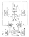
- Fig. 1 is an overall functional block diagram of the transient current peak detector.
- a device under test (DUT) 20 can be a very large scale integrated circuit which has many logic circuits 22 located within the interior of the chip area which obtained their power from a first voltage source 26 for internal circuits, which is connected by means of line 27 to the pad 23 on the chip.
- Located along the periphery of the DUT 20 will be large driver circuits such as the off-chip drivers (OCDS) 24 which receive digital signals from the interior logic circuits 22, amplify those signals and present them at signal pads along the periphery of the chip for communication to outside circuits.
- OCDS off-chip drivers
- many chip designs include a separate, independent voltage source 28 for external circuits which will provide the power for external circuits such as OCDs 24.
- the second voltage source 28 will provide its power over line 29 to the pad 25 for distribution to the external circuits on the chip, such as the OCDs 24.
- the current pulse analog pick-up circuit 30 or 30′ is shown in a more detailed illustration in Fig. 2.
- the multiplexer 34 is provided as shown in more detail in Fig. 3, which accepts line 32 from the first current pulse analog pick-up circuit 30 and it accepts line 32′ from the second current pulse analog pick-up circuit 30′.
- the multiplexer 34 can automatically direct a current pulse representation on either line 32 or line 32′ to its output 35.
- the automatic test equipment (ATE) testing computer 38 has control line 39 to the multiplexer 34, to select whether the multiplexer will exclusively focus on analog pick-up circuit 30 or analog pick-up circuit 30′ or alternately automatically select a signal from either 30 or 30′.
- ATE automatic test equipment
- the analog signal output from the multiplexer 34 on line 35 is applied to the digital peak detector 36 which is shown in greater detail in Fig. 5.
- the digital peak detector circuit 36 will capture the output of the analog section 30 or 30′, it will digitize and digitally store the peak voltage which occurs during a test period, and will provide that peak magnitude in analog form at the output 37.
- the output 37 can be applied to the ATE 38 or it can alternately be provided to other utilization devices.
- a special power distribution circuit 42 is provided which is shown in greater detail in Fig. 4.
- the power distribution circuit 42 provides operating voltage on line 43 to the analog pick-up circuit 30 and 30′, on line 45 to the multiplexer 34, in line 47 to the digital peak detector 36.
- Circuits characterized as digital circuits are separately powered from other circuits characterized as analog circuits in the analog pick-up circuit 30, 30′, the multiplexer 34, and the digital peak detector circuit 36.
- FIG. 3 shows the multiplexer circuit wherein the +5 volt analog voltage is supplied on line 45a and the ground analog voltage is supplied on line 45a′. This is from a different portion of the power distribution circuit in Fig. 4 than is the +5 volt digital voltage supplied on line 45d and the ground digital voltage as supplied on line 45d′. A similar notation is used for line 47 to the digital peak detector circuit 36 of Fig. 5.
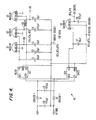
- Fig. 4 shows how the needed voltage sources of +5 volts analog, +5 volts digital, and +8 volts analog are provided. Note that analog and digital grounds are kept separate to prevent noise coupling.
- DC1 and DC2 are commercially available DC to DC converters. When the DC to DC converters are provided with five volts input voltage they provide +15 volts (unregulated and ungrounded) outputs. Separate DC to DC converters were used for the analog and digital portions of the circuit.
- High power Schottky barrier diodes D1 and D2 were placed in the +5 volt source provided by the tester and in the +5 volt return path to the tester.
- Voltage regulators V1, V2, V3, and V4 along with their associated capacitors provide the regulated voltage sources needed by the rest of the circuit.
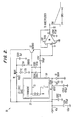
- Fig. 2 shows the current pulse analog pick-up circuit 30 or 30′ used to capture the positive peak of an Idd current transient and hold it for 20 microseconds.
- Component 50 is a shielded current transducer that provides a one-to-one current to voltage conversion of current transients and has a response time of 500 picoseconds over a frequency range 1.2 KHz to 200 MHz.
- the conducting line 27 that provides Idd, is passed through the current sensing coil 31.
- the case of the transducer 50 is raised one diode drop above analog ground by diode D1.
- Diode D1 provides thermal correction and signal bias to correct for the diode voltage drop caused by the base emitter junction of transistor Q1.
- the output of coil 31 is terminated by 50 ohm resistor combination of R204 and R205 and the base of Q1.
- Transistor Q1 charges capacitor C207 (300 pf polystyrene) to a voltage analogous to the positive peak of the Idd current transient on line 27. Once C207 is charged, the charge is trapped by the back biased base emitter junction of Q1.
- the only discharge path for C207 is a very small constant current (10 nA) into the non-inverting input of operational amplifier 51. Less than one percent of the charge stored on C207 discharges in 10 microseconds.
- Capacitors C201 and C202 provide decoupling of the +5 volts applied to resistor R203. Capacitors C203 and C204 provide decoupling of voltage developed across Q1. Capacitors C201 and C202 also provide decoupling of the +5 volts applied from line 43a to the collector of Q1 and to one side of resistor R202. Resistor R202 limits the current that flows through D1 and adjusts the bias point of Q1 to match the base emitter junction of Q1 when at the verge of conduction. The value of R202 is determined by selecting a value that causes a very small positive voltage (20 mV) at the emitter of Q1 when Idd is zero.
- Capacitor C208 (47 pf) on pin 8 of amplifier 51 over-damps the response of amplifier 51 to assure that there is no voltage overshoot applied to the digital section 36.
- the declining ramp voltage waveform at output 32 is shown in Fig. 2. Its amplitude is proportional to the charge stored on capacitor C207 due to detected Idd peaks large enough to make Q1 conduct.
- Fig. 3 shows how the output from two analog peak detectors 30 and 30′ are multiplexed into one digital peak detector 36.
- the multiplexing is done by multiplexer 34 in such a way as to provide three modes of operation, all under control of ATE 38.
- the first mode is the automatic mode in which the multiplexer 34 will automatically select whichever analog peak detector 30 or 30′ is at the higher voltage.
- the second mode always selects circuit 30 for Idd internal.
- the third and final mode always selects circuit 30′ for Idd external.
- Threshold detector 52 is a comparator connected to the outputs 32 and 32′ of both the Idd internal analog detector 30 depicted as "INT” and the output of the Idd external analog detector 30′ depicted as "EXT” via resistors R4 and R3, respectively.
- Resistor R5 provides pull-up for the output of the detector 52.
- R1, R3 and C1 provide needed hysteresis to prevent oscillation when INT and EXT are equal in voltage.
- the output of detector 52 is a logical one when EXT is greater than INT.
- the output of detector 52 is a logical zero when INT is greater than EXT.
- the three NOR gates provided by SN5428 provide logic control of the circuit and are driven by the ATE 38 over lines 39. See truth table in Fig. 3.
- the output of pin 13 of SN5428 is the logical inversion of the output of detector 52 and will control FET switch (DG301) 54 such that the output pins 2 and 13 will always be connected to whichever input 32′ (EXT) or 32 (INT) is larger. If logic control line “A” is one and “B” is zero, the output will be locked to input 32 (INT). If logic control line “B” is one, the output will be locked to 32′ (EXT) regardless of the logic state of control line "A.”
- the analog section 30 or 30′ of the peak detector will retain peaks for relatively long periods of time.
- the analog section 30 or 30′ will lose 20 mV (one LSB) in 600 microseconds.
- the multiplexer 34 will switch in less than 2 microseconds. Hence there is no loss of accuracy introduced by the multiplexer 34 when used as described.
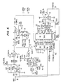
- Fig. 5 shows the circuit 36 used to capture the output of the analog section 30 or 30′, digitize and digitally store the peak voltage that occurs during the test period.
- the output of the analog section 30 or 30′ is simultaneously applied to the input (pin 1) of ADC1 analog-to-digital converter (ADC1) 64 and to the non-inverting input of comparator 56.
- Comparator 58 serves as an astable 500 KHz multivibrator that provides 5 microsecond clock pulses needed by the rest of the circuit.
- Digital-to-analog converter (DAC1) 66 in conjunction with operational amplifier 62 converts the output of analog-to-digital converter 64 back into an analog voltage.
- the hysteresis characteristic is needed to prevent comparator 56 from responding to noise which would otherwise cause the circuit to track C207 of Fig. 2 as it slowly discharges.
- the logical 1 provided by comparator 56 is inverted by the NOR gate N1 and logical 0 is applied to pin 8 of NOR gate N3. With pin 8 of N3 at logical 0, the inverted clock pulses that are always provided at pin 9 of N3 from the inverting NOR N2, are allowed to pass through N3. Once out of N3 the clock pulses are applied to pin 11 of NOR gate N4. If FET switch 60 is closed and provides a logical 0 to pin 12 of N4, the clock pulses are once again inverted and appear at pin 13 of N4 and pin 6 of analog-to-digital converter 64.
- analog-to-digital converter 64 When analog-to-digital converter 64 receives negative going clock transitions at pin 6, it converts the analog voltage at pin 1 to an eight bit digital representation of that voltage on pins 2, 3, 4, 5, 14, 15, 16, 17. The digital output from analog- to-digital converter 64 is fed directly into the digital-to-analog converter 66 where it is converted back into an analog voltage (+20 mV accuracy). Resistor R313 provides a small positive offset to the output of operational amplifier 62 so that the output of 37 is always 20 mV more positive than the voltage that was just converted. The analog signal thus produced at 37 is fed back to comparator 56 on pin 2, the inverting side.
- the output comparator 56 switches to a logical zero, blocking any clock pulses from N2. A portion of the logical 0 (0 volts) at the output of comparator 56 is fed back via R302 again providing the needed hysteresis, this time in the negative direction.
- analog-to-digital converter 64 no longer receives clock pulses (negative transitions) it simply holds the eight bit digital value of the last voltage it converted when it was last receiving negative transitions.
- Each bit of the eight bit output of analog-to-digital converter 64 is stored in a respective output flip-flop 68. Hence the circuit serves as a digital latch remembering the largest voltage applied to the input pin 1 of analog-to-digital converter 64.
- FET switch 60 provides a means to reset the circuit to the minimum value.
- the test program running in ATE 38 stops any switching of the device under test 20 for a period of 5 milliseconds or longer to allow the analog section 30 or 30′ to discharge to the minimum value (20 mV); then the tester 38 applies a logical 1 (+5 volts) on line 40 to pin 6 of FET switch 60 for at least 1 millisecond. This will force a positive transition at pin 13 causing analog-to-digital converter 64 to sample and hold the minimum voltage that is being applied at its pin 1.
- Capacitor C308 and resistor R316 establish a time constant that provides noise immunity and prevents false resets.
- the first of these programs is a subroutine entitled peakidd to condition the peak detector to clear its memory and make it ready to detect current transients, to select mode of operation (internal Idd/external Idd), to select the type of current transducer used, and to read the resulting output.
- the second program is a utility entitled findidd that uses the "peakidd" program to perform a modified binary search that will find the first occurrence of a peak current pulse in a LSSD buffer.
- the address thus found can be used to determine what element in an integrated circuit device is causing large current transients.
- Fig. 6 is a graph of the transfer function of the overall circuit. Notice the very close agreement between the response to a very long pulse (500 ns) and very short pulses (4 ns).
- the solid line drawn through the dots provides an accuracy of ten percent +100 mA over the range extending from 100 mA to 4 amps.
- Single event current pulses less than 3 ns cannot be detected to full accuracy; however, if the pulse occurs repeatedly and with a repetition rate of less than 500 microseconds, current transients of sub-nanosecond duration can be accurately measured.
- the Idd peak detector can be mounted on a circular ring printed circuit board that attaches to the center of a tester performance board. It can be used with an elevated module socket or it can be used with wafer probes.
- the current transducers 50 are pluggable and can be turned over to measure negative current. Double ended pogo pins are used to complete the current path through the transducers, facilitating easy removal and minimizing lead length.
- the resulting invention enables the VLSI automatic test equipment to detect and measure single event Idd current surges in the range of 50 milliamps to 4 amps that occur in CMOS devices and that typically last on the order of just a few nanoseconds.
Landscapes
- Engineering & Computer Science (AREA)
- Power Engineering (AREA)
- Physics & Mathematics (AREA)
- General Physics & Mathematics (AREA)
- Tests Of Electronic Circuits (AREA)
- Measurement Of Current Or Voltage (AREA)
Applications Claiming Priority (2)
| Application Number | Priority Date | Filing Date | Title |
|---|---|---|---|
| US429736 | 1989-10-18 | ||
| US07/429,736 US4965512A (en) | 1989-10-18 | 1989-10-18 | Transient current peak detector |
Publications (3)
| Publication Number | Publication Date |
|---|---|
| EP0423451A2 true EP0423451A2 (de) | 1991-04-24 |
| EP0423451A3 EP0423451A3 (en) | 1992-02-26 |
| EP0423451B1 EP0423451B1 (de) | 1995-01-18 |
Family
ID=23704520
Family Applications (1)
| Application Number | Title | Priority Date | Filing Date |
|---|---|---|---|
| EP90115285A Expired - Lifetime EP0423451B1 (de) | 1989-10-18 | 1990-08-09 | Spitzenstromdetektor |
Country Status (4)
| Country | Link |
|---|---|
| US (1) | US4965512A (de) |
| EP (1) | EP0423451B1 (de) |
| JP (1) | JPH0721514B2 (de) |
| DE (1) | DE69016151T2 (de) |
Cited By (1)
| Publication number | Priority date | Publication date | Assignee | Title |
|---|---|---|---|---|
| DE4229770A1 (de) * | 1992-09-05 | 1994-03-10 | Asea Brown Boveri | Verfahren zur Messung der transienten wiederkehrenden Spannung eines Stromkreises und Vorrichtung zur Durchführung des Verfahrens |
Families Citing this family (7)
| Publication number | Priority date | Publication date | Assignee | Title |
|---|---|---|---|---|
| US5130578A (en) * | 1989-11-30 | 1992-07-14 | Hughes Aircraft Company | Efficient high speed N-word comparator |
| US5483170A (en) * | 1993-08-24 | 1996-01-09 | New Mexico State University Technology Transfer Corp. | Integrated circuit fault testing implementing voltage supply rail pulsing and corresponding instantaneous current response analysis |
| US5760598A (en) * | 1996-02-12 | 1998-06-02 | International Business Machines Corporation | Method and apparatus for testing quiescent current in integrated circuits |
| US5923097A (en) * | 1997-07-24 | 1999-07-13 | International Business Machines Corporation | Switching supply test mode for analog cores |
| US6239586B1 (en) * | 1998-06-10 | 2001-05-29 | Hubbell Incorporated | System for digital measurement of breakdown voltage of high voltage samples |
| JP2012018037A (ja) * | 2010-07-07 | 2012-01-26 | Nec Energy Devices Ltd | 電圧測定回路及び方法 |
| WO2020126575A1 (en) | 2018-12-17 | 2020-06-25 | Ams Ag | Current peak sensor for pulsed laser diode array |
Family Cites Families (11)
| Publication number | Priority date | Publication date | Assignee | Title |
|---|---|---|---|---|
| US2836356A (en) * | 1952-02-21 | 1958-05-27 | Hughes Aircraft Co | Analog-to-digital converter |
| US3656152A (en) * | 1970-02-16 | 1972-04-11 | Hughes Aircraft Co | Improved a-d/d-a converter system |
| US3766411A (en) * | 1970-11-27 | 1973-10-16 | Intermedcraft Corp | Peak detector |
| US3777263A (en) * | 1972-02-17 | 1973-12-04 | Eastern Co | Peak holding circuit |
| SE358736B (de) * | 1972-09-15 | 1973-08-06 | Teleplan Ab | |
| US4121119A (en) * | 1977-02-16 | 1978-10-17 | Tektronix, Inc. | Pulse peak detector |
| US4246571A (en) * | 1978-03-23 | 1981-01-20 | The United States Of America As Represented By The Secretary Of The Navy | High resolution quantizer |
| US4401898A (en) * | 1980-09-15 | 1983-08-30 | Motorola Inc. | Temperature compensated circuit |
| US4560940A (en) * | 1983-06-10 | 1985-12-24 | Magnetic Peripherals Inc. | Peak amplitude measurement |
| US4613769A (en) * | 1984-08-13 | 1986-09-23 | National Semiconductor Corporation | Direct current coupled peak to peak detector circuit |
| EP1874443A4 (de) | 2005-04-29 | 2009-09-16 | Univ Rochester | Ultradünne poröse nanoskalige membranen, herstellungsverfahren dafür und verwendungen davon |
-
1989
- 1989-10-18 US US07/429,736 patent/US4965512A/en not_active Expired - Fee Related
-
1990
- 1990-08-09 EP EP90115285A patent/EP0423451B1/de not_active Expired - Lifetime
- 1990-08-09 DE DE69016151T patent/DE69016151T2/de not_active Expired - Fee Related
- 1990-10-02 JP JP2263229A patent/JPH0721514B2/ja not_active Expired - Lifetime
Cited By (1)
| Publication number | Priority date | Publication date | Assignee | Title |
|---|---|---|---|---|
| DE4229770A1 (de) * | 1992-09-05 | 1994-03-10 | Asea Brown Boveri | Verfahren zur Messung der transienten wiederkehrenden Spannung eines Stromkreises und Vorrichtung zur Durchführung des Verfahrens |
Also Published As
| Publication number | Publication date |
|---|---|
| US4965512A (en) | 1990-10-23 |
| DE69016151D1 (de) | 1995-03-02 |
| EP0423451B1 (de) | 1995-01-18 |
| EP0423451A3 (en) | 1992-02-26 |
| JPH0721514B2 (ja) | 1995-03-08 |
| DE69016151T2 (de) | 1995-06-29 |
| JPH03138570A (ja) | 1991-06-12 |
Similar Documents
| Publication | Publication Date | Title |
|---|---|---|
| US6175230B1 (en) | Circuit-board tester with backdrive-based burst timing | |
| US5053698A (en) | Test device and method for testing electronic device and semiconductor device having the test device | |
| JP2008157971A (ja) | サンプリングタイミング信号発生器 | |
| US4965512A (en) | Transient current peak detector | |
| JP4713581B2 (ja) | 比較器フィードバックピーク検出器 | |
| US20060273820A1 (en) | Input and output circuit an integrated circuit and method for testing the same | |
| US5696773A (en) | Apparatus for performing logic and leakage current tests on a digital logic circuit | |
| US20070146183A1 (en) | High-speed digital multiplexer | |
| US4743842A (en) | Tri-state circuit tester | |
| CN101297209A (zh) | 具有测试电路的模拟ic和用于这种ic的测试方法 | |
| EP0436358B1 (de) | Integrierte Schaltung mit einem die Unversehrtheit eines Energiequellenanschlusses überprüfenden Monitors | |
| US11047904B2 (en) | Low power mode testing in an integrated circuit | |
| EP1020731A2 (de) | Direktmessvorrichtung um Zwangspegel betriebsicher zu halten | |
| JP4150402B2 (ja) | 信号波形測定装置及び信号波形測定システム | |
| EP1070260B1 (de) | Anordnung für spitzenstrom prüfung einer digitalen elektronischen cmos schaltung | |
| US7360139B2 (en) | Semiconductor component, arrangement and method for characterizing a tester for semiconductor components | |
| US20030220758A1 (en) | Method for testing an AD-converter | |
| Aigner | Embedded at-speed test probe | |
| CN121679410A (zh) | 可检测显示面板裂缝的测试电路和测试方法 | |
| JP2000055978A (ja) | Cmos集積回路の電源電流測定装置 | |
| JPH07260836A (ja) | 閾値測定回路 | |
| JPH0964737A (ja) | D/a変換器及びその試験方法 |
Legal Events
| Date | Code | Title | Description |
|---|---|---|---|
| PUAI | Public reference made under article 153(3) epc to a published international application that has entered the european phase |
Free format text: ORIGINAL CODE: 0009012 |
|
| 17P | Request for examination filed |
Effective date: 19901213 |
|
| AK | Designated contracting states |
Kind code of ref document: A2 Designated state(s): DE FR GB |
|
| PUAL | Search report despatched |
Free format text: ORIGINAL CODE: 0009013 |
|
| AK | Designated contracting states |
Kind code of ref document: A3 Designated state(s): DE FR GB |
|
| 17Q | First examination report despatched |
Effective date: 19930924 |
|
| GRAA | (expected) grant |
Free format text: ORIGINAL CODE: 0009210 |
|
| AK | Designated contracting states |
Kind code of ref document: B1 Designated state(s): DE FR GB |
|
| REF | Corresponds to: |
Ref document number: 69016151 Country of ref document: DE Date of ref document: 19950302 |
|
| ET | Fr: translation filed | ||
| PLBE | No opposition filed within time limit |
Free format text: ORIGINAL CODE: 0009261 |
|
| STAA | Information on the status of an ep patent application or granted ep patent |
Free format text: STATUS: NO OPPOSITION FILED WITHIN TIME LIMIT |
|
| 26N | No opposition filed | ||
| PGFP | Annual fee paid to national office [announced via postgrant information from national office to epo] |
Ref country code: FR Payment date: 19970808 Year of fee payment: 8 |
|
| PG25 | Lapsed in a contracting state [announced via postgrant information from national office to epo] |
Ref country code: FR Free format text: LAPSE BECAUSE OF NON-PAYMENT OF DUE FEES Effective date: 19990430 |
|
| REG | Reference to a national code |
Ref country code: FR Ref legal event code: ST |
|
| PGFP | Annual fee paid to national office [announced via postgrant information from national office to epo] |
Ref country code: GB Payment date: 19990728 Year of fee payment: 10 |
|
| PGFP | Annual fee paid to national office [announced via postgrant information from national office to epo] |
Ref country code: DE Payment date: 19990816 Year of fee payment: 10 |
|
| PG25 | Lapsed in a contracting state [announced via postgrant information from national office to epo] |
Ref country code: GB Free format text: LAPSE BECAUSE OF NON-PAYMENT OF DUE FEES Effective date: 20000809 |
|
| GBPC | Gb: european patent ceased through non-payment of renewal fee |
Effective date: 20000809 |
|
| PG25 | Lapsed in a contracting state [announced via postgrant information from national office to epo] |
Ref country code: DE Free format text: LAPSE BECAUSE OF NON-PAYMENT OF DUE FEES Effective date: 20010501 |