EP0425796A2 - Vorrichtung und Verfahren diese zur Kapselung von elektronischen Modulen verwendend - Google Patents
Vorrichtung und Verfahren diese zur Kapselung von elektronischen Modulen verwendend Download PDFInfo
- Publication number
- EP0425796A2 EP0425796A2 EP90117426A EP90117426A EP0425796A2 EP 0425796 A2 EP0425796 A2 EP 0425796A2 EP 90117426 A EP90117426 A EP 90117426A EP 90117426 A EP90117426 A EP 90117426A EP 0425796 A2 EP0425796 A2 EP 0425796A2
- Authority
- EP
- European Patent Office
- Prior art keywords
- cap
- sealband
- ceramic
- substrate
- chamber
- Prior art date
- Legal status (The legal status is an assumption and is not a legal conclusion. Google has not performed a legal analysis and makes no representation as to the accuracy of the status listed.)
- Withdrawn
Links
Images


Classifications
-
- H—ELECTRICITY
- H10—SEMICONDUCTOR DEVICES; ELECTRIC SOLID-STATE DEVICES NOT OTHERWISE PROVIDED FOR
- H10P—GENERIC PROCESSES OR APPARATUS FOR THE MANUFACTURE OR TREATMENT OF DEVICES COVERED BY CLASS H10
- H10P72/00—Handling or holding of wafers, substrates or devices during manufacture or treatment thereof
- H10P72/04—Apparatus for manufacture or treatment
- H10P72/0441—Apparatus for sealing, encapsulating, glassing, decapsulating or the like
-
- H—ELECTRICITY
- H10—SEMICONDUCTOR DEVICES; ELECTRIC SOLID-STATE DEVICES NOT OTHERWISE PROVIDED FOR
- H10W—GENERIC PACKAGES, INTERCONNECTIONS, CONNECTORS OR OTHER CONSTRUCTIONAL DETAILS OF DEVICES COVERED BY CLASS H10
- H10W95/00—Packaging processes not covered by the other groups of this subclass
Definitions
- the present invention relates to the encapsulation of semiconductor chips on ceramic modules with a protective cap.
- one or more semiconductor chips which provide the main logic and memory circuits for the computer are electrically connected to a ceramic substrate.
- the ceramic substrate is in turn electrically connected to a printed circuit board and several circuit boards in the computer.
- the ceramic substrate Before the ceramic substrate is mounted on the circuit board, it is encapsulated by covering the semiconductor chips on the substrate with a protective cap, generally composed of a metallic material, which is bonded to the periphery of the ceramic substrate.
- a protective cap generally composed of a metallic material, which is bonded to the periphery of the ceramic substrate.
- the assembled ceramic substrate and metallic cap combination is called a module or module assembly.
- the encapsulation process requires large and expensive tooling, as well as a considerable amount of process time and operator attention.
- a metallic sealband typically of tin solder, silver solder or other suitable brazing material, is applied to the periphery of the substrate.
- the sealband must be flattened by placing a ceramic weight on the sealband and running the substrate-weight combination through a finely controlled furnace.
- a thermal paste is dispensed into the cap.
- a capping tool positions the metallic cap onto the substrate.
- the thermal paste acts as a thermal bridge between the semiconductor chips on the substrate and the cap to aid in heat dissipation through the cap.
- a capping fixture is then attached around the cap and substrate to apply the necessary pressure for the bonding operation.
- the substrate-cap-capping fixture combination is subsequently run through another finely controlled conveyor furnace with an inert atmosphere.
- the bonding operation is quite slow as both the module assembly and the capping fixture must be heated to the reflow temperature by means of convection heating.
- the prior art encapsulation process described above is time consuming, expensive, and requires a significant amount of floor space in the semiconductor fabrication line.
- a single conveyor furnace approx. measures 7.26 m long by 0.91 m wide, and 1.52 m high, requires constant temperature profiling throughout its lifetime.
- the combined sealband flattening and module bonding processes in such a furnace require an average of 40 minutes for each module.
- the furnaces, once profiled, remain continuously powered and are continuously purged with nitrogen or another inert gas; over time, both the power and purging gas represent significant operating costs.
- floor space on a semiconductor fabrication line is generally figured at $100 per square foot per annum, the size of the tool alone represents a significant cost factor.
- Adding yet further to the costs of the prior art encapsulation method are the multitude of capping fixtures which must be built to obtain a sufficiently high throughput.
- the capping fixtures must be specially made for each type of module assembly manufactured in the line.
- the apparatus has a substantially airtight chamber in which the ceramic substrate and cap are placed.
- a radio frequency (RF) coil acting as the inductor in the apparatus, is oriented so that the RF current induced in the cap is localized at the lip of the cap and the sealband area.
- a gas inlet port is connected to the chamber to compensate for the increase in air pressure from heated air under the cap to preserve the integrity of the molten sealband.
- the encapsulation apparatus is constructed in two major assemblies, a stationary upper assembly which includes an RF coil to provide the induction heating effect and a lower assembly having a insulator nest composed of a ceramic or other high temperature insulator, in which the ceramic substrate and cap are placed.
- the ceramic nest rests on a tool lift carriage which lifts and lowers the entire lower assembly to contact and disengage form the upper assembly.
- the components of the upper assembly are mounted on a rigid tool frame.
- the upper assembly comprises a chamber plate, a ceramic upper pressure plate and an insulator plate.
- the ceramic nest mates with the chamber plate and the ceramic upper pressure plate to form a small chamber in which the bonding process takes place.
- the ceramic upper pressure plate contacts the cap and provides the pressure necessary to assure a good bond with the substrate.
- the improved encapsulation method commences with placement of a ceramic substrate and metallic cap in the ceramic nest of the lower assembly while the apparatus is in an opened position.
- the ceramic substrate is provided with a sealband, preferably made of a solder-like material.
- the lower assembly is lifted into a closed position so that the ceramic nest is mated with the chamber plate and the ceramic upper pressure plate presses against the metallic cap.
- the RF coil is energized and produces an electromagnetic field which induces a current in the metallic cap, and sealband if the sealband is composed of a metallic material.
- the sealband is melted by the heated cap within a few seconds. When the reflow temperature of the sealband is reached, the RF coil is turned off.
- pressured nitrogen or another gas, is introduced to pressurize the chamber, equalizing the pressure on each side of sealband and thereby maintaining the integrity of the sealband.
- the module assembly is lowered to the opened position and the completed module is removed from the apparatus.
- the apparatus for disassembling as claimed comprises an RF coil oriented around an area where said cap is in contact with said sealband, said RF coil generates an electromagnetic field in RF frequency current into said cap and said sealband until said sealband is molten; and, means to separate said cap from said substrate when said sealband is molten.
- the present invention reduces the process time and costs for an encapsulation operation. Further it eliminates the need for large, expensive conventional furnace in the module encapsulation process.
- Induction heating is a method of raising the temperature of an electrically conductive material. Based on the 1831 discoveries of Michael Faraday, the temperature of a conductive material can be raised by subjecting it to an alternating electromagnetic field. The electrical currents induced in the conductive material dissipate power in the form of heat.
- a water filled coil, or inductor acts as the primary winding of a transformer and surrounds the material to be heated which acts as the secondary winding. Alternating currents flowing in the primary coil induce eddy currents in the conductive material causing it to be heated. The depth to which the eddy currents penetrate the conductive material depends on a complex relationship between the frequency of the alternating current in the inductor, the workpiece dimensions, and the magnetic permeability and resistivity of the conductive material.
- an alternating electromagnetic field in the radio-frequency (RF) spectrum of between 50kHz to 10MHz is most suitable.
- RF radio-frequency
- an RF coil is used as the inductor to produce very shallow eddy current depths (0.1 to mm) and localized heating at fast rates.
- the higher the RF frequency the shallower the eddy current and the more localized the heating effect.
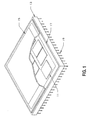
- FIG. 1 a perspective view of a completed ceramic module assembly 10 depicted.
- Semiconductor chips 11 are electrically connected to the top of the ceramic substrate 13 by means of small solder balls.
- the solder balls are attached to pads on both the chips 11 and substrate 13.
- the protective cap 15 is bonded to the periphery of the top of the substrate 13 by means of a sealband 17.
- the ceramic substrate 13 typically has a metallization feature on its top surface shaped like the sealband 17 and lip of the cap 15 to assure a good bond.
- the sealband 17 is preferably composed of a solder-like material, for example, a lead-tin or silver solder, and can be made of any brazing material compatible with the module assembly.
- the substrate 13 and cap 15 depicted in FIG. 1 measure 50mm by 50mm, however, the present invention can readily adapted to smaller and larger modules.
- a thermal paste provides a thermal bridge between the semiconductor chips 11 and the cap 15.
- connector pins 19, numbering approximately a hundred or more, are fixed to provide electric contact from the ceramic substrate 13 to a circuit board (not shown).
- the present invention will perform equally well with a substrate composed of a conventional ceramic material or the newer glass-ceramic materials to which the semiconductor industry is evolving.
- a substrate composed of a conventional ceramic material or the newer glass-ceramic materials to which the semiconductor industry is evolving.
- the term "ceramic” is used to be inclusive of both these types of substrates.
- the induction heating effect of the present invention could be used with a nonmetallic cap, inducting the RF current into the sealband 17 alone.
- a weaker RF field because of concerns of the effects of RF field on the circuitry in the semiconductor chips 11 and ceramic substrate 13, it is preferable to use a weaker RF field and rely on the induction heating effects of the field on cap 15 of which at least the cap lip is metallic. The heat generated in the cap 15 will flow to help the sealband 17 reach reflow temperature.
- the use of a metallic cap 15 shields the semiconductor and substrate circuitry from the RF induced field.
- a metallic cap or a cap with a metallic lip it is possible to use a thermoplastic, epoxy-based plastic alloy, or other polymer material for the sealband 17.
- the heat generated by the RF current induced in the cap 15 can conduct heat to the polymer sealband 17 until it reaches its reflow temperature, despite the fact that no current is induced in the sealband 17 itself.
- the use of a polymer material for the sealband would have the advantage of a lower melting point or reflow temperature, thus further reducing the chance of affecting the solder joints between the substrate 13 and the chips 13.
- the main disadvantages associated with a polymer sealband are compatibility issues with the other materials in the module assembly 10.
- a cross section view of the RF encapsulation apparatus in the opened position is shown.
- the apparatus is quite compact; with the RF generator and the heat exchanger (both not shown), it measures approximately 0.91 m wide by 0.61 m in depth by 0.76 m high.
- the apparatus replaces three conveyor furnaces which would require about 46.5 square meter in floor space, realizing a great savings in floor space in the semiconductor line.
- Ceramic substrate 13 and cap 15 are shown positioned in the ceramic nest 21 is removable from lower assembly 20.
- An O-ring 27 helps seal the chamber when the RF encapsulation apparatus is in the closed position, and a gas inlet port 29 which provides a pressurized gas mixture to the chamber during the bonding process are also shown in the lower assembly 20.
- the upper assembly 30 of the RF encapsulation apparatus is anchored by the tool frame 31 to which the other components are mounted.
- the insulator plate 33 is attached directly to the bottom of the tool frame 31. Attached to the bottom of the insulator plate 33 is the ceramic upper pressure plate 35 and the chamber plate 37.
- an RF coil 39 in the encapsulation apparatus which inducts the RF current into the lip of the cap 15 located over the sealband 17.
- the ceramic upper pressure plate 35 is located over the lip of the cap 15.
- the ceramic upper pressure plate 35 like the ceramic nest 21, is reconfigured for each size and type of substrate 13 and cap 15 to be encapsulated.
- upper pressure plate 35 and chamber plate 37 are not necessarily composed of the ceramic material, but they must be made of an insulator material to avoid coupling with a RF coil 39.
- the insulator also must be able to withstand the temperatures of 200 to 300 degrees centigrade needed to reach the reflow temperature of a solder sealband 17.
- the insulator plate 33 is not subjected to these temperatures and can be readily be made of a relatively low melting plastic.
- the RF encapsulation apparatus cross section in the closed position is depicted in Fig. 3.
- the ceramic nest 21 mates with the ceramic upper pressure plate 35 and the chamber plate 37 to form the small chamber in which the bonding process takes place.
- the O-ring 27 helps seal the chamber.
- the ceramic upper pressure plate 35 provides the pressure on the metal cap 15 necessary to create a good bond at the sealband 17, thus eliminating the need for the multitude of specialized capping fixtures and capping tools associated with prior art encapsulation processes.
- the necessary clamping force exerted by the ceramic upper pressure plate 35 is in the range of 4 to 30 kilograms.
- the apparatus operates at an RF frequency of between 400kHz to 600kHz, at approximately 2000 volts and at a power of 2 kilowatts.
- the cap 15 is made of a low expansion alloy such as Invar, a steel alloy made of 63.7% iron, 36% nickel, and 0.3% molybdenum, clad in inner and outer layers of copper. Including the copper cladding, the lip of a 50 mm by 50 mm cap measures approximately 0.66mm in thickness.
- the sealband 17 is composed of 60/40 lead/tin solder which has a reflow temperature of 194°C and is 152 ⁇ m in thickness.
- the clamping force for a 50mm by 50mm cap 15 and substrate 13 is on the order of 17-20 kilograms.
- the RF current is induced into the metallic cap 15 and solder sealband 17.
- the sealband 17 is melted within a few seconds, largely from the heat generated in the metallic cap 15 and conducted into the sealband 17 by heat transfer effects.
- the solder sealband 17 bonds to the metallization feature of the ceramic substrate 13 and the metallic lip of the cap 15.
- cap and sealband material the size of the cap 15 and the configuration of the RF coil 39 and its concentrator 43 can have a large effect on the choice of these parameters.
- the RF generator is turned off.
- a pressurized inert gas of about 41 to 55 kPa is purged through the gas inlet port 29 to equalize gas pressure on both sides of the sealband 17 until it has solidified.
- an inert gas is one which will not react with the solder 17, or other materials on chips 11 and substrate 13 such as nitrogen, helium or argon.
- the gas inlet port 29 is located in the ceramic nest 21 in this particular embodiment, its exact placement is not material to the invention so long as access to the chamber is provided.
- the lower assembly 20 is lowered and the finished module assembly 10 is unloaded from the RF encapsulation apparatus.
- the throughput of the encapsulation apparatus is dependent on a number of factors including the size of the substrate 13, cap 15 and sealband 17, the power of the RF current supplied to the RF coil 39 and the brazing material used in the sealband 17, normal cycle time for a single module assembly following the preferred embodiment described above would be on the order of 10 to 15 seconds.
- the present invention does not require the sealband flattening operation of the prior art which required an additional 15 to 20 minutes and its own specialized ceramic weights.
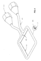
- Fig. 4 shows a perspective view of the RF coil 39 used in the preferred embodiment of the encapsulation apparatus.
- the RF coil 39 portrayed in Fig. 4 is a single turn coil made of a copper ring concentrator 43 brazed on a coil of copper tubing 44.
- a multiple turn coil could be used according to the principles of the present invention and would have an added advantage of not requiring an RF matching transformer required by the single turn coil coupled to the RF generator (both not shown).
- the single turn coil 39 is easier to incorporate and seal in the encapsulation apparatus.
- Flare nuts 41 connect the RF coil 39 to the RF generator output.
- the concentrator 43 focuses the RF current to the lip of the cap 15 and the sealband 17.
- the RF coil concentrator 43 is necessary for accurate distribution of the RF current to the lip of the cap 15 for uniform heating for the sealband 17 to control the solder flow and assure a uniform solder distribution. Without the concentrator 43, the magnetic field would be more dispersed, creating a greater chance of the circuitry on the chip 11 and substrate 13 to be affected.
- the concentrator 43 has a gap 45 to prevent shorting in the RF coil 39.
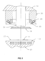
- Fig. 5 shows a modified RF encapsulation tool which can be used to disassemble a completed module assembly 10 which as failed electrical or physical testing.
- Most of the configuration remains the same as that shown in Figs. 2 and 3 except that the chamber plate 37 end O-ring 27 are no longer needed as the integrity of the sealband 17 is not an issue on rework of the module.
- the ceramic pressure plate 35 is also not required to provide pressure on the cap 15 and is modified to accept a central holder 51 which retains the cap 15 after the sealband 17 has been melted by the RF coil 39.
- the holder 51 could be a magnet for ferrous-based caps or a vacuum holder for non-ferrous caps.
- a completed module assembly 10 is placed in the ceramic nest 21, rather than an unbonded substrate an cap used above.
- the lower assembly 20 is raised until the cap 15 is in contact with the holder 51 and the pressure plate 35.
- the pressure plate 35 primarily fulfills a positioning function for the sealband 17 with respect to the RF coil 39.
- the RF coil 39 is energized by the high frequency generator and melts the sealband 17.
- the holder 51 prevents the cap 15 from descending with the substrate 13 and separation of the module assembly is accomplished. After the substrate 13 is removed, the holder 51 can be lowered to allow for easier removal of the cap 15.
Landscapes
- General Induction Heating (AREA)
- Electric Connection Of Electric Components To Printed Circuits (AREA)
- Drying Of Semiconductors (AREA)
Applications Claiming Priority (2)
| Application Number | Priority Date | Filing Date | Title |
|---|---|---|---|
| US429889 | 1989-10-31 | ||
| US07/429,889 US5182424A (en) | 1989-10-31 | 1989-10-31 | Module encapsulation by induction heating |
Publications (2)
| Publication Number | Publication Date |
|---|---|
| EP0425796A2 true EP0425796A2 (de) | 1991-05-08 |
| EP0425796A3 EP0425796A3 (en) | 1991-07-31 |
Family
ID=23705134
Family Applications (1)
| Application Number | Title | Priority Date | Filing Date |
|---|---|---|---|
| EP19900117426 Withdrawn EP0425796A3 (en) | 1989-10-31 | 1990-09-10 | Apparatus for and method using the apparatus for the encapsulation of electronic modules |
Country Status (3)
| Country | Link |
|---|---|
| US (2) | US5182424A (de) |
| EP (1) | EP0425796A3 (de) |
| JP (1) | JPH03154364A (de) |
Cited By (4)
| Publication number | Priority date | Publication date | Assignee | Title |
|---|---|---|---|---|
| WO1993008591A1 (en) * | 1991-10-25 | 1993-04-29 | Electrotech Limited | Processing system |
| EP1489392A1 (de) * | 2003-06-16 | 2004-12-22 | Siemens Aktiengesellschaft | Verfahren zur Herstellung einer elektronischen Anordnung und eine elektronische Schaltungsanordnung |
| WO2006055063A1 (en) * | 2004-11-15 | 2006-05-26 | Honeywell International Inc. | Chip packaging systems and methods |
| CN113199103A (zh) * | 2021-06-11 | 2021-08-03 | 哈尔滨工业大学 | 适用于高功率电子器件或组件的电磁感应快速连接方法 |
Families Citing this family (16)
| Publication number | Priority date | Publication date | Assignee | Title |
|---|---|---|---|---|
| US5182424A (en) * | 1989-10-31 | 1993-01-26 | Vlastimil Frank | Module encapsulation by induction heating |
| US7323666B2 (en) | 2003-12-08 | 2008-01-29 | Saint-Gobain Performance Plastics Corporation | Inductively heatable components |
| JP2005286273A (ja) * | 2004-03-31 | 2005-10-13 | Sohki:Kk | 回路基板、回路基板の製造方法、電子デバイス、電子デバイスの製造方法 |
| JP4279207B2 (ja) * | 2004-06-18 | 2009-06-17 | アルプス電気株式会社 | 入力装置およびこの入力装置を用いた表示入力装置 |
| US7414226B2 (en) * | 2004-11-19 | 2008-08-19 | General Electric Company | Movable heating method and system having fixed heating source for brazing stator bars |
| JP4995003B2 (ja) * | 2007-08-21 | 2012-08-08 | オリジン電気株式会社 | 電子部品パッケージの製造装置及び製造方法 |
| US20090056592A1 (en) * | 2007-08-31 | 2009-03-05 | Everthere Carriers, Llc | Combined cargo carrier and portable table |
| JP4894784B2 (ja) * | 2008-02-27 | 2012-03-14 | 三菱電機株式会社 | 半導体装置とその製造方法 |
| US20090314642A1 (en) * | 2008-04-25 | 2009-12-24 | Zhiyin Gan | Carbon nanotubes bonding on metallic electrodes |
| US7763976B2 (en) * | 2008-09-30 | 2010-07-27 | Freescale Semiconductor, Inc. | Integrated circuit module with integrated passive device |
| US20130119051A1 (en) * | 2011-11-02 | 2013-05-16 | Apple Inc. | Directed heating for component rework |
| TW201414559A (zh) * | 2012-10-08 | 2014-04-16 | Power Mate Technology Co Ltd | 金屬外罩與板體之焊接方法 |
| CN205159286U (zh) | 2012-12-31 | 2016-04-13 | 菲力尔系统公司 | 用于微辐射热计真空封装组件的晶片级封装的装置 |
| US9508680B1 (en) | 2015-06-17 | 2016-11-29 | Globalfoundries Inc. | Induction heating for underfill removal and chip rework |
| US9947560B1 (en) * | 2016-11-22 | 2018-04-17 | Xilinx, Inc. | Integrated circuit package, and methods and tools for fabricating the same |
| CN116313838B (zh) * | 2023-03-07 | 2023-07-28 | 天津中科晶禾电子科技有限责任公司 | 三维封装方法及三维封装装置 |
Family Cites Families (32)
| Publication number | Priority date | Publication date | Assignee | Title |
|---|---|---|---|---|
| US3536568A (en) * | 1966-12-08 | 1970-10-27 | Willcox & Gibbs Inc | Sealing and/or severing device for plastic films |
| US3651299A (en) * | 1970-06-22 | 1972-03-21 | Continental Can Co | Method for sealing containers using heat activated magnetic sealing compound |
| US3808074A (en) * | 1970-11-06 | 1974-04-30 | United Glass Ltd | Induction heat sealing of a container |
| US3706176A (en) * | 1971-03-10 | 1972-12-19 | Alfred F Leatherman | Closure member and method for closing containers |
| US3783218A (en) * | 1972-01-12 | 1974-01-01 | Gen Electric | Electrostatic bonding process |
| US3781978A (en) * | 1972-05-16 | 1974-01-01 | Gen Electric | Process of making thermoelectrostatic bonded semiconductor devices |
| US3872275A (en) * | 1973-12-12 | 1975-03-18 | Thermatool Corp | Forge welding with induction coil heating |
| US3993123A (en) * | 1975-10-28 | 1976-11-23 | International Business Machines Corporation | Gas encapsulated cooling module |
| US4079511A (en) * | 1976-07-30 | 1978-03-21 | Amp Incorporated | Method for packaging hermetically sealed integrated circuit chips on lead frames |
| FR2416078A2 (fr) * | 1976-10-05 | 1979-08-31 | Tocco Stel | Presse a braser par induction des pieces metalliques comportant des portions peripheriques incurvees ou relevees |
| US4069498A (en) * | 1976-11-03 | 1978-01-17 | International Business Machines Corporation | Studded heat exchanger for integrated circuit package |
| US4154998A (en) * | 1977-07-12 | 1979-05-15 | Trw Inc. | Solar array fabrication method and apparatus utilizing induction heating |
| JPS5826828B2 (ja) * | 1978-04-26 | 1983-06-06 | 新光電気工業株式会社 | テ−プキヤリアの製造方法 |
| US4218578A (en) * | 1978-08-04 | 1980-08-19 | Burr-Brown Research Corp. | RF Shield for an electronic component |
| US4251852A (en) * | 1979-06-18 | 1981-02-17 | International Business Machines Corporation | Integrated circuit package |
| US4355463A (en) * | 1980-03-24 | 1982-10-26 | National Semiconductor Corporation | Process for hermetically encapsulating semiconductor devices |
| US4400870A (en) * | 1980-10-06 | 1983-08-30 | Texas Instruments Incorporated | Method of hermetically encapsulating a semiconductor device by laser irradiation |
| JPS5790964A (en) * | 1980-11-27 | 1982-06-05 | Sharp Corp | Sealing method for semiconductor device |
| US4380484A (en) * | 1981-02-20 | 1983-04-19 | William C. Heller, Jr. | Inductively heated tooling and method for working plastic members |
| US4392992A (en) * | 1981-06-30 | 1983-07-12 | Motorola, Inc. | Chromium-silicon-nitrogen resistor material |
| JPS58218166A (ja) * | 1982-06-14 | 1983-12-19 | Hitachi Ltd | 固体撮像装置の製造方法 |
| JPS5988016A (ja) * | 1982-11-09 | 1984-05-21 | 株式会社クボタ | 歩行型田植機 |
| US4552300A (en) * | 1983-05-09 | 1985-11-12 | Pace, Incorporated | Method and apparatus for soldering and desoldering leadless semiconductor modules for printed wiring boards |
| JPS60249349A (ja) * | 1984-05-24 | 1985-12-10 | Nec Kansai Ltd | フラツトパツケ−ジのシ−ル方法 |
| US4558171A (en) * | 1984-10-12 | 1985-12-10 | General Electric Company | Hermetic enclosure for electronic components with an optionally transparent cover and a method of making the same |
| JPS61210643A (ja) * | 1985-03-15 | 1986-09-18 | Nec Corp | 半導体組立装置 |
| US4701999A (en) * | 1985-12-17 | 1987-10-27 | Pnc, Inc. | Method of making sealed housings containing delicate structures |
| US4820658A (en) * | 1986-04-14 | 1989-04-11 | Gte Products Corporation | Method of making a packaged IC chip |
| US4814943A (en) * | 1986-06-04 | 1989-03-21 | Oki Electric Industry Co., Ltd. | Printed circuit devices using thermoplastic resin cover plate |
| US4740663A (en) * | 1987-01-02 | 1988-04-26 | Continental Can Company, Inc. | Transverse flux induction heating unit |
| US4757175A (en) * | 1987-01-02 | 1988-07-12 | Continental Can Company, Inc. | Induction heating coil |
| US5182424A (en) * | 1989-10-31 | 1993-01-26 | Vlastimil Frank | Module encapsulation by induction heating |
-
1989
- 1989-10-31 US US07/429,889 patent/US5182424A/en not_active Expired - Fee Related
-
1990
- 1990-09-10 EP EP19900117426 patent/EP0425796A3/en not_active Withdrawn
- 1990-10-05 JP JP2266597A patent/JPH03154364A/ja active Granted
-
1992
- 1992-04-30 US US07/876,345 patent/US5558795A/en not_active Expired - Fee Related
Cited By (8)
| Publication number | Priority date | Publication date | Assignee | Title |
|---|---|---|---|---|
| WO1993008591A1 (en) * | 1991-10-25 | 1993-04-29 | Electrotech Limited | Processing system |
| US5518771A (en) * | 1991-10-25 | 1996-05-21 | Electrotech Limited | Method and apparatus for subjecting a workpiece to elevated pressure |
| US5575850A (en) * | 1991-10-25 | 1996-11-19 | Electrotech Limited | Processing system |
| EP1489392A1 (de) * | 2003-06-16 | 2004-12-22 | Siemens Aktiengesellschaft | Verfahren zur Herstellung einer elektronischen Anordnung und eine elektronische Schaltungsanordnung |
| WO2004111581A3 (en) * | 2003-06-16 | 2005-04-21 | Siemens Ag | A method for manufacturing an electronic arrangement and an electronic circuit arrangement |
| WO2006055063A1 (en) * | 2004-11-15 | 2006-05-26 | Honeywell International Inc. | Chip packaging systems and methods |
| US7314777B2 (en) | 2004-11-15 | 2008-01-01 | Honeywell International Inc. | Chip packaging systems and methods |
| CN113199103A (zh) * | 2021-06-11 | 2021-08-03 | 哈尔滨工业大学 | 适用于高功率电子器件或组件的电磁感应快速连接方法 |
Also Published As
| Publication number | Publication date |
|---|---|
| EP0425796A3 (en) | 1991-07-31 |
| JPH0418467B2 (de) | 1992-03-27 |
| JPH03154364A (ja) | 1991-07-02 |
| US5558795A (en) | 1996-09-24 |
| US5182424A (en) | 1993-01-26 |
Similar Documents
| Publication | Publication Date | Title |
|---|---|---|
| US5182424A (en) | Module encapsulation by induction heating | |
| US5541524A (en) | Burn-in technologies for unpackaged integrated circuits | |
| JP4640170B2 (ja) | 半田付け方法及び半導体モジュールの製造方法並びに半田付け装置 | |
| WO1993004375A1 (en) | Burn-in technologies for unpackaged integrated circuits | |
| JPH10303473A (ja) | 多段電子冷却装置及びその製造方法 | |
| KR101004587B1 (ko) | 납땜 방법 및 반도체 모듈의 제조 방법 그리고 납땜 장치 | |
| WO2000022883A1 (en) | Matrix-inductor soldering apparatus and soldering process | |
| CN112289695A (zh) | 一种用于多焊件自动共晶的通用共晶装置及共晶方法 | |
| US20090266811A1 (en) | Soldering Apparatus and Soldering Method | |
| JPH0145231B2 (de) | ||
| CN215342513U (zh) | 一种用于单片微波集成电路芯片批量共晶焊接的装置 | |
| US5385291A (en) | Method employing an elevating of atmospheric pressure during the heating and/or cooling phases of ball grid array (BGA) soldering of an IC device to a PCB | |
| US20090134204A1 (en) | Soldering Method and Semiconductor Module Manufacturing Method | |
| US5080279A (en) | Method for tape automated bonding | |
| EP0243621B1 (de) | Lötverfahren und Gerät | |
| JP5029279B2 (ja) | 半田付け装置、半田付け方法及び電子機器の製造方法 | |
| JP2006108589A (ja) | 金属ケース付き電子部品の製造方法および製造装置 | |
| JP2008147555A (ja) | 半田付け方法及び錘並びに電子機器の製造方法 | |
| US3911569A (en) | Method and apparatus for bonding miniature semiconductor pill-type components to a circuit board | |
| JP2008140815A (ja) | 半田付け方法及び電子機器の製造方法 | |
| JP4833972B2 (ja) | 半導体構成部品を組み付ける方法 | |
| CN117444340A (zh) | 一种共晶焊方法 | |
| JPH0770563B2 (ja) | テ−プボンディング装置及び方法 | |
| JPH04151844A (ja) | アウターリードボンディング装置 | |
| JP4396199B2 (ja) | 陽極接合装置 |
Legal Events
| Date | Code | Title | Description |
|---|---|---|---|
| PUAI | Public reference made under article 153(3) epc to a published international application that has entered the european phase |
Free format text: ORIGINAL CODE: 0009012 |
|
| 17P | Request for examination filed |
Effective date: 19901213 |
|
| AK | Designated contracting states |
Kind code of ref document: A2 Designated state(s): DE FR GB IT |
|
| PUAL | Search report despatched |
Free format text: ORIGINAL CODE: 0009013 |
|
| AK | Designated contracting states |
Kind code of ref document: A3 Designated state(s): DE FR GB IT |
|
| 17Q | First examination report despatched |
Effective date: 19930909 |
|
| STAA | Information on the status of an ep patent application or granted ep patent |
Free format text: STATUS: THE APPLICATION IS DEEMED TO BE WITHDRAWN |
|
| 18D | Application deemed to be withdrawn |
Effective date: 19960822 |