EP0426111B1 - Système de commande de mémoire - Google Patents
Système de commande de mémoire Download PDFInfo
- Publication number
- EP0426111B1 EP0426111B1 EP90120801A EP90120801A EP0426111B1 EP 0426111 B1 EP0426111 B1 EP 0426111B1 EP 90120801 A EP90120801 A EP 90120801A EP 90120801 A EP90120801 A EP 90120801A EP 0426111 B1 EP0426111 B1 EP 0426111B1
- Authority
- EP
- European Patent Office
- Prior art keywords
- pointer
- memory
- increasing
- data
- block
- Prior art date
- Legal status (The legal status is an assumption and is not a legal conclusion. Google has not performed a legal analysis and makes no representation as to the accuracy of the status listed.)
- Expired - Lifetime
Links
Images




Classifications
-
- G—PHYSICS
- G06—COMPUTING OR CALCULATING; COUNTING
- G06F—ELECTRIC DIGITAL DATA PROCESSING
- G06F13/00—Interconnection of, or transfer of information or other signals between, memories, input/output devices or central processing units
- G06F13/14—Handling requests for interconnection or transfer
- G06F13/16—Handling requests for interconnection or transfer for access to memory bus
- G06F13/1605—Handling requests for interconnection or transfer for access to memory bus based on arbitration
- G06F13/1652—Handling requests for interconnection or transfer for access to memory bus based on arbitration in a multiprocessor architecture
- G06F13/1657—Access to multiple memories
-
- Y—GENERAL TAGGING OF NEW TECHNOLOGICAL DEVELOPMENTS; GENERAL TAGGING OF CROSS-SECTIONAL TECHNOLOGIES SPANNING OVER SEVERAL SECTIONS OF THE IPC; TECHNICAL SUBJECTS COVERED BY FORMER USPC CROSS-REFERENCE ART COLLECTIONS [XRACs] AND DIGESTS
- Y10—TECHNICAL SUBJECTS COVERED BY FORMER USPC
- Y10S—TECHNICAL SUBJECTS COVERED BY FORMER USPC CROSS-REFERENCE ART COLLECTIONS [XRACs] AND DIGESTS
- Y10S707/00—Data processing: database and file management or data structures
- Y10S707/99931—Database or file accessing
Definitions
- the present invention relates to a memory control system with a memory unit comprising a plurality of memory blocks which are individually accessible.
- a data processing apparatus which has a CPU 10 (first processing means) and a DMA controller 20 (second processing means) as shown in Fig. 9 so that data is directly transferred between a magnetic disk 40 and an RAM 30b under the control of the DMA controller 20, without involving the CPU 10, and during the data transfer, the CPU 10 executes another processing, e.g., processing of data in an RAM 30a, thereby increasing the data processing speed.
- the CPU 10 needs only to specify, to the DMA controller 20, data to be transferred, and read/write access to the RAM 30b or the like, and execution of a program by the CPU 10 and the data transfer by the DMA controller 20 are performed in parallel.
- a disk controller 50 shown in Fig. 9 executes access control to the magnetic disk 40 under the control of the DMA controller 20.
- Cited reference EP-A-0 261 751 discloses a concurrent memory access system allowing simultaneous access to a memory 16 by any two of a digitiser 12, a display controller 18 and a microprocessor 24.
- the memory 16 is organised into an "odd"-bank 16a for storing data at all of the odd-memory addresses of the memory space and an "even"-bank for storing data in all even-memory addresses of the memory space.
- Each bank is independently accessible in the sense that each communicates independently of the MMU 14 through separate data, address and control lines.
- a data processing device such as digitiser 12, display controller 18 or microprocessor 24
- the banks 16a and 16b are accessed in an alternating fashion.
- each data processing device is able to write a data sequence into (or read a data sequence out of) memory 16 without substantially interfering with the rate at which the other device writes about a sequence (or reads a data sequence out of) the memory.
- memory management unit 14 converts the interfering access demands from the different data processing devices (digitiser 12, display controller 18, microprocessor 24) to ensure that two competing devices access different memory banks 16a, 16b at the same time.
- Fig. 1 is a block diagram illustrating the arrangement of a memory control system embodying the present invention.
- This memory control system has a first processor 2 connected to a magnetic disk 1 for storing a transaction file or the like and a second processor 4 connected to a magnetic disk 3 for storing a master file or the like. Both apparatuses 2 and 4 are connected via a bus selecting circuit 5 to an RAM 6 including a plurality of memory blocks. These apparatuses 2 and 4 are also commonly connected to a pointer memory 7 that stores various types of pointers.
- the first processor 2 is capable of accessing one memory block in the RAM 6, which is specified by the first pointer P 1 of the pointer memory 7, to update data in the associated memory block based on data of the transaction file stored on the disk 1.
- the second processor 4 is capable of accessing one memory block in the RAM 6, which is specified by the second pointer P 2 of the pointer memory 7, to read out data from that memory block and transfer it to the disk 3.
- the RAM 6 includes four memory blocks #1, #2, #3 and #4, with a bus line (including a control bus line and data bus line) connected to each block, so that these memory blocks are separately accessible.
- the addresses of the individual memory blocks, which can serve as independent memories are contiguous and their address regions have address "00000 - 3FFFF,” "40000 - 7FFFF,” “80000 - BFFFF” and "C0000 - FFFFF" in order from the first memory block #1. It is therefore possible to store in each memory block data contiguous over a plurality of memory blocks, permitting the whole memory blocks to be treated as if it were a single memory.
- the bus switching circuit 5 connects the bus line of the specified memory block to the bus line of the first processor 2.
- the bus switching circuit 5 connects the bus line of this specified memory block to the bus line of the second processor 4.
- Fig. 2 is a detailed block diagram of the bus switching circuit 5.
- the bus lines from the individual memory blocks #1 to #4 are connected to one side of the selectors 51 to 54 provided in association with these memory blocks.
- the bus lines from the first processor 2 and the second processor 4 are selectably connected to selectors 51 to 54 on the other side.
- a memory block designating signal P 1 from the first processor 2 is input to a decoder 55 which in turn decodes its value to output one of acknowledge signals P 11 to P 14 .
- a memory block designating signal P 2 from the second processor 4 is input to a decoder 56 which in turn decodes its value to output one of acknowledge signals P 21 to P 24 .
- the selector 51 Upon reception of the acknowledge signal P 11 from the decoder 55, the selector 51 connects the bus line from the memory block #1 to the bus line from the first processor 2 to allow the first processor 2 to access this memory block #1. Upon reception of the acknowledge signal P 21 from the decoder 56, the selector 51 connects the bus line from the memory block #1 to the bus line from the second processor 4 to allow memory access to this memory block #1 from the second processor 4.
- the other selectors 52-54 function in exactly the same manner as the selector 51.
- the content of the master file stored over the individual memory blocks in the RAM 6 is updated by the transaction file on the disk 1 connected to the first processor 2, and the updated content of the master file is transferred for storage onto the disk 3 connected to the second processor 4.
- Fig. 3 is a flowchart illustrating the processing performed by the first processor 2 in the above operation.
- the first processor 2 starts the processing according to the flowchart shown in Fig. 3.
- the first processor 2 specifies a memory block corresponding to the first pointer P 1 (step A1). That is, the first processor 2 reads out the value of the first pointer P 1 from the pointer memory 7 and sends the value to the decoder 55 of the bus switching circuit 5.
- the decoder 55 in turn decodes the value of the first pointer P 1 , "1" in this case, and sends the acknowledge signal P 11 to the selector 51.
- the selector 51 connects the bus line from the memory block #1 to the bus line from the first processor 2.
- step A2 every data in the specified memory block is updated.
- the first processor 2 accesses the memory block #1 to sequentially read out data therefrom, updates the data based on data in the transaction file on the disk 1, and writes the updated data again into the memory block #1.
- step A3 it is determined whether or not the first pointer P 1 is an end pointer, i.e., whether or not the value of the pointer P 1 is "4" indicating the last memory block #4.
- step A4 the flow advances to step A4 where the first pointer P 1 is incremented or (P 1 + 1 ⁇ P 1 ) is computed and the incremented first pointer P 1 is written in the pointer memory 7.
- step A4 the flow returns to step A1.
- the first pointer P 1 is incremented to "2" in step A4 and the second memory block #2 is specified in step A1.
- the same routines are repeated thereafter and the entire processing is terminated when it is determined in step A3 that the first pointer P 1 specifies the last memory block #4.
- the first processor 2 sequentially accesses the memory blocks from #1 to #4 and updates data using the transaction file stored on the disk 1.
- Fig. 4 is a flowchart illustrating the processing of the second processor 4.
- step B1 it is determined in step B1 whether or not the second pointer P 2 in the pointer memory 7 is smaller than the first pointer P 1 .
- This step B1 is repeated until the second pointer P 2 becomes smaller than the first pointer P 1 or until the first processor 2 updates the data in the specified memory block, incrementing the first pointer P 1 .
- the flow advances to step B2 where a memory block corresponding to the second pointer P 2 is specified. That is, the second processor 4 reads out the value of the second pointer P 2 from the pointer memory 7 and sends the value to the decoder 56 of the bus switching circuit 5.
- the decoder 56 in turn decodes the value of the second pointer P 2 , "1" in this case, and sends the acknowledge signal P 21 to the selector 51.
- the selector 51 connects the bus line from the memory block #1 to the bus line from the second processor 4.
- the flow then advances to step B3 where the second processor 2 accesses the specified memory block, sequentially reads out all the pieces of data in this memory block and transfers them to the disk 3.
- step B4 it is determined whether or not the second pointer P 2 is an end pointer, i.e., whether or not the value of the pointer P 2 is "4" indicating the last memory block #4. If the determination is negative (NO), the flow advances to step B5 where the second pointer P 2 is incremented.
- the second processor 4 checks if data updating to this memory block has been performed by the first processor 2, and, if the determination is affirmative, sequentially accesses the updated memory block and transfers the content to the disk 3.
- the first processor 2 and second processor 4 can separately access each memory block. Even before the first processor 2 has not completed updating every data in the RAM 6, if there is any memory block in the RAM 6 whose data updating has already been completed, the second processor 4 can access this memory block. In other words, the first processor 2 and second processor 4 can execute simultaneous or parallel processing, resulting in high speed processing.
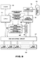
- Fig. 5 presents a block structural diagram of the data updating apparatus which comprises a CPU 11, a data transfer controller 12, RAMs 13 and 14, a magnetic disk 15, a disk controller 16, a read block pointer RP, a write block pointer WP, a process block pointer UP, and a selector 18.
- the CPU 11 controls processing, such as registering of, for example, daily total data developed in the RAM 13 into a total file, and adding the daily total data in the total file to previous total data in a monthly total file which is developed in the RAM 14.
- the data transfer controller 12 transfers data between the magnetic disk 15 and the RAM 14 in response to a command from the CPU 11. In this case, the data transfer controller 12 transfers data to the RAM 14 from the magnetic disk 15 upon reception of a read command from the CPU 11, and transfers data to the magnetic disk from the RAM 14 upon reception of a write command. This data transfer is executed block by block as will be described later.
- the data transfer controller 12 only controls data transfer, and it is the disk controller 16 that accesses the magnetic disk 15.
- the RAM 14 is divided into a plurality of memory blocks, which can individually be accessed through bus switching conducted by a bus switching circuit 17.
- the bus switching circuit 17 switches the buses, so that the CPU 11 can access the block to which data reading has already been completed.
- the CPU 11 executes a data updating process on the data in this accessible memory block. Even during the data updating, the data transfer controller 12 keeps reading data into the remaining blocks.
- the read block pointer RP, the write block pointer WP, and the process block pointer UP are utilized for such a control.
- the selector 18 selects either the read block pointer RP or the write block pointer WP and outputs it to the bus switching circuit 17.
- As the bus switching circuit 17 has the same structure as the bus switching circuit 5 in Fig. 2, its description will be omitted.
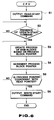
- the CPU 11 sets an initial value "1" to the process block pointer UP, and sends a read-start command to the data transfer controller 12 (step S1).
- the CPU 11 then waits for an update-start command from the data transfer controller 12 (step S2).
- the CPU 11 Upon reception of the update-start command from the data transfer controller 12, the CPU 11 performs predetermined update processing on data in that block in the RAM 14 which has the block number specified by the process block pointer UP (step S3).
- step S4 the content of the process block pointer UP is incremented by "1" (step S4), and it is determined whether or not the content of the process block pointer UP coincides with the content of the read block pointer RP (step S5).
- the CPU 11 sends a write-start command to the data transfer controller 12 (step S6), terminating the whole operation.
- the data transfer controller 12 sets an initial value "1" to the read block pointer RP and the write block pointer WP, and waits for a read-start command from the CPU 11 (step S51).
- the data transfer controller 12 reads data to be updated from the magnetic disk 15 into that block in the RAM 14 which is specified by the read block pointer RP (step S52).
- the content of the read block pointer UP is incremented by "1" (step S53), and an update-start command is sent to the CPU 11 (step S54).
- step S55 it is determined whether or not data to be updated, which should be read in, is present on the magnetic disk 15 (step S55).
- the data transfer controller 12 reads data to be updated from the magnetic disk 15 into a block indicated by the read block pointer RP (step S56). After reading data for one block, the content of the read block pointer RP is incremented by "1" (step S57), and the flow returns to step S55.
- step S55 If it is determined in step S55 that no further to-be-updated data, which should be read in, remains on the magnetic disk 15, or when the to-be-updated data is read in, the data transfer controller 12 waits for a write-start command from the CPU (step S58).
- the data transfer controller 12 On receiving the write-start command, the data transfer controller 12 transfers data in a block indicated by the write block pointer WP, or the data for one block updated by the CPU 11, to the magnetic disk 15 (step S59). After the transfer of the data for one block, the content of the write block pointer WP is incremented by "1" (step S60).
- step S61 it is determined whether or not the contents of the write block pointer WP and the read block pointer RP coincide with each other.
- the data transfer controller 12 terminates the whole operation.
- the CPU 11 outputs a read-start command to the data transfer controller 12 (see “a” in Fig. 8).
- the data transfer controller 12 (simply referred to as FCU 12 in the diagram) in turn reads data into the block having the block number indicated by the read block pointer RP (see “b” and “c”).
- the data transfer controller 12 sends an update-start command to the CPU 11 upon completion of reading data into the first block.
- the CPU 11 executes data updating, such as adding data in the RAM 13 to that data read in the block which is specified by the process block pointer UP (see “d” and “e”).
- data updating such as adding data in the RAM 13 to that data read in the block which is specified by the process block pointer UP (see “d” and “e”).
- the reading of data in the specified block by the data transfer controller 12 and the data updating to this read data by the CPU 11 are executed in parallel, as should be apparent from the diagram.
- the CPU 11 sends a write-start command to the data transfer controller 12 (see “f").
- the data transfer controller 12 Upon reception of this write-start command, the data transfer controller 12 transfers updated data in the block specified by the write block pointer WP to the magnetic disk 15 (see “g” and "h”). When the content of the write block pointer WP coincides with that of the read block pointer RP, the data transfer controller 12 stops transferring the updated data.
- the data read-in process and the data updating on the read data are simultaneously executed in parallel in the above manner.
- the data updating should not necessarily be performed from that block into which data has already been read; the data updating can be executed in any order as long as data reading in the target blocks has been completed.
Landscapes
- Engineering & Computer Science (AREA)
- Theoretical Computer Science (AREA)
- Physics & Mathematics (AREA)
- General Engineering & Computer Science (AREA)
- General Physics & Mathematics (AREA)
- Information Retrieval, Db Structures And Fs Structures Therefor (AREA)
Claims (4)
- Un système de commande de mémoire comportant des moyens de mémoire qui comprennent un ensemble de blocs de mémoire (6), chaque bloc de mémoire étant accessible individuellement, comprenant :(A) des premier et second moyens de traitement (2, 4) que l'on peut faire fonctionner séparément; et(B) des moyens de mémoire de pointeurs (7) pour enregistrer un premier pointeur (P1) et un second pointeur (P2); dans lequel(C) les premiers moyens de traitement comprennent des premiers moyens de spécification (Etape A1) pour spécifier l'un des blocs de mémoire au moyen du premier pointeur, des premiers moyens d'accès (Etape A2) pour accéder au bloc de mémoire spécifié, des premiers moyens d'augmentation (Etape A4) pour augmenter le premier pointeur, et des premiers moyens de répétition pour répéter les opérations de spécification, d'accès et d'augmentation qui sont effectuées par les premiers moyens de spécification, les premiers moyens d'accès et les premiers moyens d'augmentation: et(D) les seconds moyens de traitement comprennent des moyens de comparaison (Etape B1) pour comparer le premier pointeur et le second pointeur, des seconds moyens de spécification (Etape B2) pour spécifier l'un des blocs de mémoire au moyen du second pointeur, lorsque le second pointeur est inférieur au premier pointeur, des seconds moyens d'accès (Etape B3) pour accéder à un bloc de mémoire spécifié par le second pointeur, des seconds moyens d'augmentation (Etape B5) pour augmenter le second pointeur, et des seconds moyens de répétition pour répéter les opérations de comparaison, de spécification, d'accès et d'augmentation qui sont effectuées par les moyens de comparaison, les seconds moyens de spécification, les seconds moyens d'accès et les seconds moyens d'augmentation.
- Le système de commande de mémoire selon la revendication 1, caractérisé en ce que(E) les premiers moyens de répétition comprennent des moyens pour répéter les opérations de spécification, d'accès et d'augmentation jusqu'à ce que l'on ait accédé à tous les blocs de mémoire nécessaires; et(F) les seconds moyens de répétition comprennent des moyens pour répéter les opérations de comparaison, de spécification, d'accès et d'augmentation jusqu'å ce que le second pointeur coïncide avec le premier pointeur.
- Le système de commande de mémoire selon la revendication 1, caractérisé en ce que(G) les premiers moyens de spécification comprennent des premiers moyens de connexion pour connecter une ligne bus de l'un des blocs de mémoire correspondant au premier pointeur, à une ligne bus des premiers moyens de traitement; et(H) les seconds moyens de spécification comprennent en outre des seconds moyens de connexion pour connecter la ligne bus de l'un des blocs de mémoire correspondant au second pointeur, à une ligne bus des seconds moyens de traitement.
- Un système de commande de mémoire, comprenant :(A) des moyens de mémoire externes (15) pour enregistrer un ensemble de blocs de données;(B) des moyens de mémoire internes (14), comprenant un ensemble de blocs de mémoire et qui sont accessibles individuellement, bloc par bloc;(C) des moyens de mémoire de pointeurs pour enregistrer un premier pointeur (POINTEUR DE BLOC DE LECTURE), un second pointeur (POINTEUR DE BLOC DE TRAITEMENT) et un troisième pointeur (POINTEUR DE BLOC D'ECRITURE);(D) des moyens de commande de transfert de données (12); et(E) des moyens d'actualisation de données (11); dans lequel(F) les moyens de commande de transfert de données comprennent des moyens de lecture (Etape S52, S56) pour lire l'un des blocs de données dans les moyens de mémoire externes, des moyens d'enregistrement pour enregistrer le bloc de données lu dans l'un des blocs de mémoire correspondant au premier pointeur, des premiers moyens d'augmentation (Etape S53, S57) pour augmenter le premier pointeur, lorsque l'enregistrement est terminé, et des premiers moyens de répétition, pour répéter, jusqu'à l'absence de bloc de données à lire, les opérations de lecture, d'enregistrement et d'augmentation qui sont effectuées par les moyens de lecture, les moyens d'enregistrement et les premiers moyens d'augmentation;(G) les moyens d'actualisation de données comprennent des moyens d'actualisation (Etape S3) pour actualiser, lorsque le second pointeur est inférieur au premier pointeur, un bloc de données enregistré dans l'un des blocs de mémoire correspondant au second pointeur, des seconds moyens d'augmentation (Etape S4) pour augmenter le second pointeur, lorsque l'actualisation est terminée, et des seconds moyens de répétition pour répéter l'actualisation et l'augmentation qui sont effectuées par les moyens d'actualisation et les seconds moyens d'augmentation, jusqu'à ce que le second pointeur coïncide avec le premier pointeur; et(H) les moyens de commande de transfert de données comprennent en outre des moyens d'écriture (Etape S59) pour écrire dans les moyens de mémoire externes le bloc de données actualisé qui est enregistré dans l'un des blocs de mémoire correspondant au troisième pointeur, des troisièmes moyens d'augmentation (Etape S60) pour augmenter le troisième pointeur, lorsque l'écriture est terminée, et des troisièmes moyens de répétition pour répéter l'écriture et l'augmentation qui sont effectuées par les moyens d'écriture et les troisièmes moyens d'augmentation, jusqu'à ce que le troisième pointeur coïncide avec le premier pointeur.
Applications Claiming Priority (2)
| Application Number | Priority Date | Filing Date | Title |
|---|---|---|---|
| JP1285658A JPH03147013A (ja) | 1989-11-01 | 1989-11-01 | データ更新装置 |
| JP285658/89 | 1989-11-01 |
Publications (3)
| Publication Number | Publication Date |
|---|---|
| EP0426111A2 EP0426111A2 (fr) | 1991-05-08 |
| EP0426111A3 EP0426111A3 (en) | 1992-03-18 |
| EP0426111B1 true EP0426111B1 (fr) | 1997-10-01 |
Family
ID=17694386
Family Applications (1)
| Application Number | Title | Priority Date | Filing Date |
|---|---|---|---|
| EP90120801A Expired - Lifetime EP0426111B1 (fr) | 1989-11-01 | 1990-10-30 | Système de commande de mémoire |
Country Status (4)
| Country | Link |
|---|---|
| US (1) | US5210852A (fr) |
| EP (1) | EP0426111B1 (fr) |
| JP (1) | JPH03147013A (fr) |
| DE (1) | DE69031529T2 (fr) |
Families Citing this family (9)
| Publication number | Priority date | Publication date | Assignee | Title |
|---|---|---|---|---|
| JPH04363745A (ja) * | 1991-05-17 | 1992-12-16 | Toshiba Corp | Dmaコントローラ |
| DE69316559T2 (de) * | 1992-12-03 | 1998-09-10 | Advanced Micro Devices Inc | Servoregelkreissteuerung |
| JPH07121181A (ja) * | 1993-10-27 | 1995-05-12 | Sony Corp | 音声情報処理装置 |
| US5946696A (en) * | 1996-05-31 | 1999-08-31 | Microsoft Corporation | Object property lists |
| US5774135A (en) * | 1996-11-05 | 1998-06-30 | Vlsi, Technology, Inc. | Non-contiguous memory location addressing scheme |
| US6026417A (en) * | 1997-05-02 | 2000-02-15 | Microsoft Corporation | Desktop publishing software for automatically changing the layout of content-filled documents |
| JP5235692B2 (ja) * | 2009-01-15 | 2013-07-10 | 三菱電機株式会社 | データアクセス装置及びデータアクセスプログラム |
| US8671082B1 (en) * | 2009-02-26 | 2014-03-11 | Netapp, Inc. | Use of predefined block pointers to reduce duplicate storage of certain data in a storage subsystem of a storage server |
| WO2017056310A1 (fr) * | 2015-10-02 | 2017-04-06 | 株式会社日立製作所 | Ordinateur et procédé de commande d'un ordinateur |
Family Cites Families (9)
| Publication number | Priority date | Publication date | Assignee | Title |
|---|---|---|---|---|
| US3955180A (en) * | 1974-01-02 | 1976-05-04 | Honeywell Information Systems Inc. | Table driven emulation system |
| US4495569A (en) * | 1982-06-28 | 1985-01-22 | Mitsubishi Denki Kabushiki Kaisha | Interrupt control for multiprocessor system with storage data controlling processor interrupted by devices |
| US4636974A (en) * | 1983-10-04 | 1987-01-13 | Hughes Aircraft Company | Method and apparatus for transferring data between operationally-juxtaposed memories and knowledge-retrieving systems utilizing same |
| US4855903A (en) * | 1984-12-20 | 1989-08-08 | State University Of New York | Topologically-distributed-memory multiprocessor computer |
| US4837688A (en) * | 1986-07-25 | 1989-06-06 | International Business Machines Corporation | Multi-channel shared resource processor |
| US4805094A (en) * | 1986-08-27 | 1989-02-14 | American Telephone & Telegraph Company | Multi-channel memory access circuit |
| EP0261751A3 (fr) * | 1986-09-25 | 1990-07-18 | Tektronix, Inc. | Système d'accès de mémoire concurrent |
| US4818932A (en) * | 1986-09-25 | 1989-04-04 | Tektronix, Inc. | Concurrent memory access system |
| US4967392A (en) * | 1988-07-27 | 1990-10-30 | Alliant Computer Systems Corporation | Drawing processor for computer graphic system using a plurality of parallel processors which each handle a group of display screen scanlines |
-
1989
- 1989-11-01 JP JP1285658A patent/JPH03147013A/ja active Pending
-
1990
- 1990-10-23 US US07/602,097 patent/US5210852A/en not_active Expired - Fee Related
- 1990-10-30 DE DE69031529T patent/DE69031529T2/de not_active Expired - Fee Related
- 1990-10-30 EP EP90120801A patent/EP0426111B1/fr not_active Expired - Lifetime
Also Published As
| Publication number | Publication date |
|---|---|
| DE69031529T2 (de) | 1998-02-19 |
| EP0426111A3 (en) | 1992-03-18 |
| DE69031529D1 (de) | 1997-11-06 |
| EP0426111A2 (fr) | 1991-05-08 |
| JPH03147013A (ja) | 1991-06-24 |
| US5210852A (en) | 1993-05-11 |
Similar Documents
| Publication | Publication Date | Title |
|---|---|---|
| US6272596B1 (en) | Data processor | |
| EP0054243A2 (fr) | Appareil de commande de mémoire | |
| JPH0814801B2 (ja) | プログラマブルアクセスメモリ | |
| US4371924A (en) | Computer system apparatus for prefetching data requested by a peripheral device from memory | |
| US5034885A (en) | Cache memory device with fast data-write capacity | |
| EP0426111B1 (fr) | Système de commande de mémoire | |
| EP0167089B1 (fr) | Système de commande et procédé d'accèss en mémoire pour un appareil de traitement d'informations | |
| US5388230A (en) | Parallel processor having multi-processing units either connected or bypassed in either series or parallel by the use of bus switching | |
| EP1026600B1 (fr) | Procédé et dispositif d'interface de mémoire à accès aléatoire | |
| US4314332A (en) | Memory control system | |
| US5012410A (en) | Data processor with instruction cache memory | |
| US4737908A (en) | Buffer memory control system | |
| US4561071A (en) | Storage system having buffer storage | |
| US5704056A (en) | Cache-data transfer system | |
| JP3222647B2 (ja) | メモリバンク自動切替システム | |
| JP3144979B2 (ja) | プログラム処理装置及び処理方法 | |
| JPS6043764A (ja) | 情報処理システム | |
| JP2581144B2 (ja) | バス制御装置 | |
| JPH04127227A (ja) | メモリ制御システム | |
| JPS58111171A (ja) | メモリアクセス方式 | |
| JPS6373458A (ja) | 共有メモリアクセス装置 | |
| JPH04359336A (ja) | キャッシュメモリのデータ置換回路 | |
| JPS6340954A (ja) | 記憶装置 | |
| JPH0528414B2 (fr) | ||
| JPS6134656A (ja) | バス選択装置 |
Legal Events
| Date | Code | Title | Description |
|---|---|---|---|
| PUAI | Public reference made under article 153(3) epc to a published international application that has entered the european phase |
Free format text: ORIGINAL CODE: 0009012 |
|
| AK | Designated contracting states |
Kind code of ref document: A2 Designated state(s): DE FR GB IT NL |
|
| 17P | Request for examination filed |
Effective date: 19910322 |
|
| PUAL | Search report despatched |
Free format text: ORIGINAL CODE: 0009013 |
|
| AK | Designated contracting states |
Kind code of ref document: A3 Designated state(s): DE FR GB IT NL |
|
| 17Q | First examination report despatched |
Effective date: 19950123 |
|
| GRAG | Despatch of communication of intention to grant |
Free format text: ORIGINAL CODE: EPIDOS AGRA |
|
| GRAH | Despatch of communication of intention to grant a patent |
Free format text: ORIGINAL CODE: EPIDOS IGRA |
|
| GRAH | Despatch of communication of intention to grant a patent |
Free format text: ORIGINAL CODE: EPIDOS IGRA |
|
| GRAA | (expected) grant |
Free format text: ORIGINAL CODE: 0009210 |
|
| AK | Designated contracting states |
Kind code of ref document: B1 Designated state(s): DE FR GB IT NL |
|
| ITF | It: translation for a ep patent filed | ||
| REF | Corresponds to: |
Ref document number: 69031529 Country of ref document: DE Date of ref document: 19971106 |
|
| ET | Fr: translation filed | ||
| RAP2 | Party data changed (patent owner data changed or rights of a patent transferred) |
Owner name: CASIO COMPUTER CO., LTD. |
|
| NLT2 | Nl: modifications (of names), taken from the european patent patent bulletin |
Owner name: CASIO COMPUTER CO., LTD. |
|
| PLBE | No opposition filed within time limit |
Free format text: ORIGINAL CODE: 0009261 |
|
| STAA | Information on the status of an ep patent application or granted ep patent |
Free format text: STATUS: NO OPPOSITION FILED WITHIN TIME LIMIT |
|
| 26N | No opposition filed | ||
| PGFP | Annual fee paid to national office [announced via postgrant information from national office to epo] |
Ref country code: FR Payment date: 19991011 Year of fee payment: 10 |
|
| PGFP | Annual fee paid to national office [announced via postgrant information from national office to epo] |
Ref country code: GB Payment date: 19991027 Year of fee payment: 10 |
|
| PGFP | Annual fee paid to national office [announced via postgrant information from national office to epo] |
Ref country code: NL Payment date: 19991029 Year of fee payment: 10 |
|
| PGFP | Annual fee paid to national office [announced via postgrant information from national office to epo] |
Ref country code: DE Payment date: 19991102 Year of fee payment: 10 |
|
| PG25 | Lapsed in a contracting state [announced via postgrant information from national office to epo] |
Ref country code: GB Free format text: LAPSE BECAUSE OF NON-PAYMENT OF DUE FEES Effective date: 20001030 |
|
| PG25 | Lapsed in a contracting state [announced via postgrant information from national office to epo] |
Ref country code: NL Free format text: LAPSE BECAUSE OF NON-PAYMENT OF DUE FEES Effective date: 20010501 |
|
| GBPC | Gb: european patent ceased through non-payment of renewal fee |
Effective date: 20001030 |
|
| PG25 | Lapsed in a contracting state [announced via postgrant information from national office to epo] |
Ref country code: FR Free format text: LAPSE BECAUSE OF NON-PAYMENT OF DUE FEES Effective date: 20010629 |
|
| NLV4 | Nl: lapsed or anulled due to non-payment of the annual fee |
Effective date: 20010501 |
|
| PG25 | Lapsed in a contracting state [announced via postgrant information from national office to epo] |
Ref country code: DE Free format text: LAPSE BECAUSE OF NON-PAYMENT OF DUE FEES Effective date: 20010703 |
|
| REG | Reference to a national code |
Ref country code: FR Ref legal event code: ST |
|
| PG25 | Lapsed in a contracting state [announced via postgrant information from national office to epo] |
Ref country code: IT Free format text: LAPSE BECAUSE OF NON-PAYMENT OF DUE FEES Effective date: 20051030 |