EP0437129A2 - Dispositif à semi-conducteurs de type à carte - Google Patents
Dispositif à semi-conducteurs de type à carte Download PDFInfo
- Publication number
- EP0437129A2 EP0437129A2 EP90403584A EP90403584A EP0437129A2 EP 0437129 A2 EP0437129 A2 EP 0437129A2 EP 90403584 A EP90403584 A EP 90403584A EP 90403584 A EP90403584 A EP 90403584A EP 0437129 A2 EP0437129 A2 EP 0437129A2
- Authority
- EP
- European Patent Office
- Prior art keywords
- power source
- source voltage
- semiconductor device
- battery
- voltage
- Prior art date
- Legal status (The legal status is an assumption and is not a legal conclusion. Google has not performed a legal analysis and makes no representation as to the accuracy of the status listed.)
- Granted
Links
Images





Classifications
-
- G—PHYSICS
- G11—INFORMATION STORAGE
- G11C—STATIC STORES
- G11C5/00—Details of stores covered by group G11C11/00
- G11C5/14—Power supply arrangements, e.g. power down, chip selection or deselection, layout of wirings or power grids, or multiple supply levels
- G11C5/143—Detection of memory cassette insertion or removal; Continuity checks of supply or ground lines; Detection of supply variations, interruptions or levels ; Switching between alternative supplies
-
- G—PHYSICS
- G11—INFORMATION STORAGE
- G11C—STATIC STORES
- G11C5/00—Details of stores covered by group G11C11/00
- G11C5/14—Power supply arrangements, e.g. power down, chip selection or deselection, layout of wirings or power grids, or multiple supply levels
- G11C5/141—Battery and back-up supplies
-
- H—ELECTRICITY
- H02—GENERATION; CONVERSION OR DISTRIBUTION OF ELECTRIC POWER
- H02J—ELECTRIC POWER NETWORKS; CIRCUIT ARRANGEMENTS OR SYSTEMS FOR SUPPLYING OR DISTRIBUTING ELECTRIC POWER; SYSTEMS FOR STORING ELECTRIC ENERGY
- H02J9/00—Circuit arrangements for emergency or stand-by power supply, e.g. for emergency lighting
- H02J9/04—Circuit arrangements for emergency or stand-by power supply, e.g. for emergency lighting in which the distribution system is disconnected from the normal source and connected to a standby source
- H02J9/06—Circuit arrangements for emergency or stand-by power supply, e.g. for emergency lighting in which the distribution system is disconnected from the normal source and connected to a standby source with automatic change-over, e.g. UPS systems
- H02J9/061—Circuit arrangements for emergency or stand-by power supply, e.g. for emergency lighting in which the distribution system is disconnected from the normal source and connected to a standby source with automatic change-over, e.g. UPS systems for DC powered loads
Definitions
- the present invention relates to a card type semiconductor device, for example, a memory card device or an IC card including a microprocessor, for use in the field of portable personal computers, word processors, and other systems, and more particularly relates to a memory card device having a memory device which requires a constant supply of power for holding data, and a countermeasure means against disconnection of a battery terminal.
- memory cards carrying secondary batteries suffer from a decline in their charging efficiency when the secondary batteries have been over-discharged and require a long time for charging to the voltage required for holding the memory data.
- Figure 1 is a schematic view of a conventional memory card.
- the conventional memory card is comprised of a primary battery 1 which is not rechargeable, for supplying current for holding data to the memory 5 during separation from a system 7, a secondary battery 2 which is rechargeable, for supplying current for holding data to the memory 5 during replacement of the primary battery 1, and a switching control unit 31 for controlling the circuit switching to supply power to the memory 5 and the secondary battery 2 from the system 7 side during mounting in the system 7.
- the primary battery is a battery such as a lithium cell which is used as a back-up cell and which can be exchanged when consumed
- the secondary battery is a battery such a cadmium cell which is built into the memory card device, cannot be exchanged, and must be charged as soon as possible when an operator begins to use the system, for example, a personal computer, in which the battery is used.
- the present invention was made to resolve the above problems and has as its object the provision of a memory card type semiconductor device wherein it is possible to replace a primary battery immediately after a fall in the potential of the primary battery even before mounting in a system and wherein it is possible to charge a secondary battery for backing up the first battery in an extremely short time.
- a card type semiconductor device including a terminal for receiving an external power source voltage, a semiconductor device operatively connected to the terminal, a primary battery for supplying a first power source voltage, a secondary battery for supplying a second power source voltage, a first switching means for supplying the first power source voltage from the primary battery to the semiconductor device, when the external power source voltage is not supplied, a second switching means for supplying the second power source voltage from the secondary battery to the semiconductor device, when the first power source voltage is not supplied, and means for charging the secondary battery by the first power source voltage supplied from the primary battery.
- the secondary power source is charged from the system power source and the primary power source during mounting in the system, the secondary power source is charged from the primary power source during separation from the system, and current for holding the data is supplied from the secondary power source to the memory device during replacement of the primary power source, it is possible to fully charge the secondary power source immediately before mounting in the system or in a short time after mounting and to smoothly replace to just power source. Further, when the system is battery driven, it is possible to prevent reduction of the power source lifetime of the system.
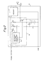
- Figure 2 is a schematic view of a memory card of the present embodiment
- Figs. 3(A) and (B) are views for explaining the operation of the embodiment.
- the memory card of the present embodiment is comprised of a primary battery 1, secondary battery which is rechargeable 2, and memory 5 housed in a card body 6.
- the memory 5 is a volatile memory such as a static RAM, a dynamic RAM or the like. When a microprocessor chip or a power source is turned off, the memory contents are not maintained.
- the present invention also includes a card device which contains ICs, or semiconductor devices.
- the memory card of the embodiment is provided with a diode 4 connected so that the direction of current from the primary battery 1 to the secondary battery 2 is biased forward between the output sides of the primary battery 1 and the secondary battery 2 and a switching control circuit 31 which detects the potential levels of the primary battery 1 and the secondary battery 2 and controls the connections among the primary battery 1, the secondary battery 2, the memory 5, and the system 7.
- the above-mentioned switching control unit 31 is provided with a reference voltage detecting circuit 31A which compares the potential levels of the primary battery 1, secondary battery 2, and the power supply potential V cc of the system 7 side with a predetermined reference potential, a transistor 31B for supplying current for holding data from the power supply of the system 7 to the memory 5, a transistor 31C for issuing a warning, based on the results of the comparison of the above-mentioned voltage detecting circuit 31A, to the effect that the drive state has been entered and the primary battery 1 should be exchanged, a diode 31D connected so that the current supply from the primary battery 1 to the memory 5 is biased forward, and a diode 31E connected so that the current supply from the secondary battery 2 to the memory 5 side is biased forward.
- a reference voltage detecting circuit 31A which compares the potential levels of the primary battery 1, secondary battery 2, and the power supply potential V cc of the system 7 side with a predetermined reference potential
- a transistor 31B for supplying current for holding data from the
- the power source voltage of the system 7 is higher than the battery voltage delivered for maintaining data such as the primary battery 1. While the memory card 6 is mounted in the system 7 such as a personal computer, the power source voltage from the system 7 is supplied to the secondary battery through a reference voltage detecting circuit 31A and a connection node X. A voltage higher than the voltage level of the primary battery is produced by a level transformation of a power source voltage V cc from the system 7 side.
- the secondary battery supplies a power source voltage to the memory 5 until the voltage of the secondary battery becomes lower than that of the primary battery.
- the supply of power from the primary battery to the memory 5 is minimized advantageously.
- Figure 4 is a view for explaining the charging operation of the present embodiment in comparison with the prior art.
- the transistor 31B When mounting the memory card in the system 7, whether or not the power supply voltage V cc of the system 7 has reached a predetermined reference potential value or more is determined by the reference voltage detecting circuit 31A. If over the reference potential value, the transistor 31B enters a drive state to give the connection configuration shown in Fig. 3(A) and the switch in the reference voltage detecting circuit 31A (illustration omitted in Fig. 2) is turned on. Due to the connection configuration of Fig. 3(A), current for holding the data is supplied from the power supply of the system 7 through the transistor 31B in the drive state to the memory 5. Further, charging current is supplied through the on state switch from the power supply of the system 7 to the secondary battery 2.
- the supply of charging current to the secondary battery 2 may also be performed by supplying current from the primary battery 1 along with the current of the system 7 side (see hatching portion of Fig. 4(B)) so as to speedily charge the battery and to reduce the power consumption of the system 7 as much as possible.
- the reference voltage detecting circuit 31A determines whether or not the potential level of the battery 1 is higher than a predetermined current required for holding the data. If above the predetermined potential, current for holding the data is supplied from the primary battery 1 to the memory 5. Further, at the above potential level, whether or not the potential of the primary battery 1 is higher than the potential of the secondary battery 2 is determined by the reference voltage detecting circuit 31A. During the time when the potential of the primary battery 1 is higher, the diode 4 is forward biased and charging current is supplied from the primary battery 1 to the secondary battery 2.
- the reference voltage detecting circuit 31A discriminates that the potential level of the primary battery 1 is below a predetermined value, a signal indicating a drop in the voltage is output to the buzzer 8 and the memory card device produces a warning signals to warn that the primary battery 1 should be replaced.
- a diode 4 was connected to the outside of the power control unit 3, but as shown in Fig. 5, as one of the functions of the power control unit 3, it is possible to make the construction so as to supply power for charging the secondary battery 2 from the battery 1 at all times when the potential of the battery 1 is higher than the potential of the secondary battery 2. Further, it is possible to construct this as an IC (integrated circuit device) providing a diode 4 in the power control unit 3.
- IC integrated circuit device
- an alarm terminal ALM was provided and an alarm signal was output based on the operation of the reference voltage detecting circuit 31A, but it is also possible to leave out these functions and to simplify the construction.
- the secondary power source is charged from the system power source and the primary power source during mounting in the system, the secondary power source is charged from the primary power source during separation from the system, and current for holding the data is supplied from the secondary power source to the memory during replacement of the primary power source, the effect is exhibited that it is possible to fully charge the secondary power source immediately before mounting in the system or in a short time after mounting and to smoothly replace a power source. Further, when the system is battery driven, it is possible to prevent reduction of the power source lifetime of the system.
- Fig. 7 is a timing chart of an input/output voltage and an alarm operation.
- a voltage level of an input power source voltage V IN an output voltage V OUT is produced to provide a RESET signal to each of LOGIC, SRAM, and ROM in 5.
- V INH a voltage level of V INH
- a RESET voltage V 1 is output.
- V INL a voltage level of V INL
- a RESET voltage V2 (slightly higher than ground level) is output.
- the RESET signal When an input power source voltage V IN rises, and the RESET signal surpasses the voltage level V INH or is lower than the voltage level V INL , the RESET signal is output (a "HIGH" level voltage).
- Fig. 7(B) is a timing chart showing an alarm operation when a power supply source turns ON.
- a primary battery voltage V SAT drops to lower than both voltage levels V SATH1 and V SATH2 , or for a period until it rises to surpass both voltage levels V SATL1 and V SATL2 , each alarm signal ALARM1, ALARM2 outputs a "LOW" level voltage.
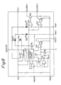
- FIG 8 is a detailed circuit diagram of a switching control unit IC11 in Fig. 6, where V SENSE and BUFFER terminals are not used.
- SBD(*2) and SBD(*3) correspond to diodes 31E, 31D in Fig. 2.
- Figure 9 is a timing chart of a system including a memory card device in accordance with the present invention.
- waveforms of each signal are shown for a case when the system accesses a memory card.
- an access signal is produced from a system, and a card power source type B is chosen, an address signal, an I/O signal, a control signal and a charging period are produced accordingly.
- the system power source supplies power only when a card is accessed.
- the charging of a secondary battery 2 depends on an access from the system to the card and so the charging time of the battery is not constant.
- the charging does not depend on supplying power from the system to the card. Since the charging of the secondary battery can be effected more smoothly with the primary battery connected to the card, the above problem can be solved easily.
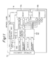
- Figure 10 is a block diagram of a memory card including a memory such as a 256K SRAM.
- Reference numeral 110 denotes an input buffer
- 111A and 111B denote SRAM
- 112 denotes an input/output buffer
- 113 denotes a switching control unit.
- a plurality of SRAMs are mounted in a memory card, although two memories 111A and 111B are illustrated.
- the input buffer 110 has two functions. First, signals input from a system, for example, input address A1 to A15 are amplified to be supplied to a built-in IC circuit in a card. Second, chip select signals CS0 ⁇ CS15 for selecting a plurality of SRAMs are produced using the signals A0, A16 ⁇ A18 input from the system 7.
- the input/output buffer 112 is an interface which inputs or outputs data from the system 7 to the SRAM and vice versa.
- a control line 1 includes signals WE(write enable), OE(output enable), CSL, CSH, WP SW, WP in Fig. 10, a high order address A0, A16 to A18, a low order address A1 to A15, data 1, 2 for I/O0 to I/O15, a control line 2 for chip-select signals CS0 to CS15, and an address A1 to A15, respectively.
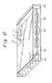
- Fig. 12 is an oblique projection drawing with a partial cross-sectional view of an IC card in accordance with the present invention.
- Reference numeral 1 denotes a primary battery, 2 a secondary battery, 6 the overall IC card, 61 connector pins, 62 a connector portion, 60 a printed circuit board, 63 a semiconductor chip, 64 a cover plate, and 65 a card frame.
Landscapes
- Engineering & Computer Science (AREA)
- Power Engineering (AREA)
- Business, Economics & Management (AREA)
- Emergency Management (AREA)
- Power Sources (AREA)
- Techniques For Improving Reliability Of Storages (AREA)
- Credit Cards Or The Like (AREA)
Applications Claiming Priority (2)
| Application Number | Priority Date | Filing Date | Title |
|---|---|---|---|
| JP1321535A JPH0823793B2 (ja) | 1989-12-13 | 1989-12-13 | メモリカード |
| JP321535/89 | 1989-12-13 |
Publications (3)
| Publication Number | Publication Date |
|---|---|
| EP0437129A2 true EP0437129A2 (fr) | 1991-07-17 |
| EP0437129A3 EP0437129A3 (en) | 1992-03-18 |
| EP0437129B1 EP0437129B1 (fr) | 1996-04-10 |
Family
ID=18133648
Family Applications (1)
| Application Number | Title | Priority Date | Filing Date |
|---|---|---|---|
| EP90403584A Expired - Lifetime EP0437129B1 (fr) | 1989-12-13 | 1990-12-13 | Dispositif à semi-conducteurs de type à carte |
Country Status (4)
| Country | Link |
|---|---|
| EP (1) | EP0437129B1 (fr) |
| JP (1) | JPH0823793B2 (fr) |
| KR (1) | KR940001490B1 (fr) |
| DE (1) | DE69026487T2 (fr) |
Cited By (12)
| Publication number | Priority date | Publication date | Assignee | Title |
|---|---|---|---|---|
| WO1993007555A1 (fr) * | 1991-10-08 | 1993-04-15 | Smartdiskette Gmbh | Dispositif de lecture et d'ecriture pour disquette intelligente |
| US5270972A (en) * | 1992-04-14 | 1993-12-14 | Xicor, Inc. | Three terminal serial-communicating peripheral device |
| WO1993020488A3 (fr) * | 1992-03-31 | 1994-03-31 | Dow Chemical Co | Systeme d'interface destine aux automatismes industriels dote d'ordinateurs de terrain a triple redondance |
| EP0657982A1 (fr) * | 1993-11-26 | 1995-06-14 | Nec Corporation | Système d'utilisation d'une batterie pour un équipement électrique portable |
| GB2292866A (en) * | 1994-08-30 | 1996-03-06 | Mitsubishi Electric Corp | Power supply for non-contact IC card |
| EP0734546A4 (fr) * | 1993-12-17 | 1997-08-20 | Berg Tech Inc | Moyen de traitement de donnees, son circuit de sauvegarde et son systeme de traitement des donnees |
| US5761061A (en) * | 1993-12-17 | 1998-06-02 | Berg Technology, Inc. | Data processing medium, its backup circuit, and data processing system |
| EP1352443A2 (fr) | 2000-12-22 | 2003-10-15 | Jumpit AS | Batterie de reserve destinee a un telephone cellulaire |
| EP1042827A4 (fr) * | 1997-12-02 | 2007-10-17 | Tadiran Batteries Ltd | Batteries composites et procedes de fabrication |
| WO2011057845A1 (fr) * | 2009-11-10 | 2011-05-19 | Sb Limotive Company Ltd. | Système batterie doté de différents types d'éléments |
| US12393244B2 (en) | 2022-12-20 | 2025-08-19 | Samsung Electronics Co., Ltd. | Systems, methods, and apparatus for providing power to storage devices |
| US12578777B2 (en) | 2022-12-20 | 2026-03-17 | Samsung Electronics Co., Ltd. | Systems, methods, and apparatus for providing power to storage devices |
Family Cites Families (3)
| Publication number | Priority date | Publication date | Assignee | Title |
|---|---|---|---|---|
| JPS61160185A (ja) * | 1985-01-08 | 1986-07-19 | Nippon Telegr & Teleph Corp <Ntt> | 電池内蔵icカ−ド |
| GB2205697A (en) * | 1987-06-11 | 1988-12-14 | Chloride Group Plc | Automotive electric storage battery power system |
| US4779037A (en) * | 1987-11-17 | 1988-10-18 | National Semiconductor Corporation | Dual input low dropout voltage regulator |
-
1989
- 1989-12-13 JP JP1321535A patent/JPH0823793B2/ja not_active Expired - Fee Related
-
1990
- 1990-12-13 DE DE1990626487 patent/DE69026487T2/de not_active Expired - Fee Related
- 1990-12-13 KR KR9020497A patent/KR940001490B1/ko not_active Expired - Fee Related
- 1990-12-13 EP EP90403584A patent/EP0437129B1/fr not_active Expired - Lifetime
Cited By (17)
| Publication number | Priority date | Publication date | Assignee | Title |
|---|---|---|---|---|
| WO1993007555A1 (fr) * | 1991-10-08 | 1993-04-15 | Smartdiskette Gmbh | Dispositif de lecture et d'ecriture pour disquette intelligente |
| AU660494B2 (en) * | 1991-10-08 | 1995-06-29 | Smartdiskette Gmbh | Smart-diskette read-write device |
| US5471038A (en) * | 1991-10-08 | 1995-11-28 | Smart-Diskette Gmbh | Smart-diskette read/write device having fixed head |
| WO1993020488A3 (fr) * | 1992-03-31 | 1994-03-31 | Dow Chemical Co | Systeme d'interface destine aux automatismes industriels dote d'ordinateurs de terrain a triple redondance |
| EP0869415A3 (fr) * | 1992-03-31 | 1999-12-15 | The Dow Chemical Company | Système d'interface destiné aux automatismes industriels doté d'ordinateurs de terrain à triple redondance |
| US5270972A (en) * | 1992-04-14 | 1993-12-14 | Xicor, Inc. | Three terminal serial-communicating peripheral device |
| EP0657982A1 (fr) * | 1993-11-26 | 1995-06-14 | Nec Corporation | Système d'utilisation d'une batterie pour un équipement électrique portable |
| US5568038A (en) * | 1993-11-26 | 1996-10-22 | Nec Corporation | Portable electric equipment and rechargeable built-in batteries |
| EP0734546A4 (fr) * | 1993-12-17 | 1997-08-20 | Berg Tech Inc | Moyen de traitement de donnees, son circuit de sauvegarde et son systeme de traitement des donnees |
| US5761061A (en) * | 1993-12-17 | 1998-06-02 | Berg Technology, Inc. | Data processing medium, its backup circuit, and data processing system |
| GB2292866A (en) * | 1994-08-30 | 1996-03-06 | Mitsubishi Electric Corp | Power supply for non-contact IC card |
| EP1042827A4 (fr) * | 1997-12-02 | 2007-10-17 | Tadiran Batteries Ltd | Batteries composites et procedes de fabrication |
| EP1352443A2 (fr) | 2000-12-22 | 2003-10-15 | Jumpit AS | Batterie de reserve destinee a un telephone cellulaire |
| US6709784B2 (en) | 2000-12-22 | 2004-03-23 | Jumpit As | Back-up battery for a cellular telephone |
| WO2011057845A1 (fr) * | 2009-11-10 | 2011-05-19 | Sb Limotive Company Ltd. | Système batterie doté de différents types d'éléments |
| US12393244B2 (en) | 2022-12-20 | 2025-08-19 | Samsung Electronics Co., Ltd. | Systems, methods, and apparatus for providing power to storage devices |
| US12578777B2 (en) | 2022-12-20 | 2026-03-17 | Samsung Electronics Co., Ltd. | Systems, methods, and apparatus for providing power to storage devices |
Also Published As
| Publication number | Publication date |
|---|---|
| DE69026487T2 (de) | 1996-08-22 |
| DE69026487D1 (de) | 1996-05-15 |
| EP0437129B1 (fr) | 1996-04-10 |
| KR940001490B1 (en) | 1994-02-23 |
| JPH0823793B2 (ja) | 1996-03-06 |
| JPH03184110A (ja) | 1991-08-12 |
| EP0437129A3 (en) | 1992-03-18 |
| KR910012974A (ko) | 1991-08-08 |
Similar Documents
| Publication | Publication Date | Title |
|---|---|---|
| EP0437129B1 (fr) | Dispositif à semi-conducteurs de type à carte | |
| US5545935A (en) | Rechargeable system with separate battery circuits in a common module | |
| US5706239A (en) | Rechargeable SRAM/flash PCMCIA card | |
| JPH04155417A (ja) | 機能拡張装置 | |
| US5929603A (en) | Apparatus for preventing over-discharge | |
| US5274828A (en) | Computer including an integrated circuit having an on-chip high voltage source | |
| US4823323A (en) | Electronic apparatus with replaceable power source | |
| JPS6061988A (ja) | 半導体メモリ | |
| JPS6377335A (ja) | バツクアツプ電源装置 | |
| JPS6225224B2 (fr) | ||
| JPH07230344A (ja) | 携帯型電子機器及び電池パック | |
| JPH0732542B2 (ja) | Icカードにおける二次電池への充電方式 | |
| CA1162647A (fr) | Fonctionnement en multiplex du terminal de validation d'ecriture d'un circuit de memoire pour les fonctions de controle et d'alimentation de secours | |
| EP0734546B1 (fr) | Moyen de traitement de donnees, son circuit de sauvegarde et son systeme de traitement des donnees | |
| JPH031287A (ja) | Icカード | |
| JPH01195590A (ja) | Icメモリカードの保管装置 | |
| JPS62251194A (ja) | Icカ−ド | |
| JPS62254252A (ja) | Icカ−ド | |
| JPH02193209A (ja) | メモリカード用電源装置 | |
| JPH07104900A (ja) | 電子機器 | |
| RU2020613C1 (ru) | Запоминающее устройство с сохранением информации при отключении питания | |
| JPH0333910A (ja) | 記憶機能を有するカード状体 | |
| JPH01289137A (ja) | 半導体集積回路装置 | |
| JPH0374148A (ja) | 電池を用いる電源回路 | |
| JPS60245012A (ja) | Cpuおよびメモリのバツクアツプ電源回路 |
Legal Events
| Date | Code | Title | Description |
|---|---|---|---|
| PUAI | Public reference made under article 153(3) epc to a published international application that has entered the european phase |
Free format text: ORIGINAL CODE: 0009012 |
|
| AK | Designated contracting states |
Kind code of ref document: A2 Designated state(s): DE FR GB |
|
| PUAL | Search report despatched |
Free format text: ORIGINAL CODE: 0009013 |
|
| AK | Designated contracting states |
Kind code of ref document: A3 Designated state(s): DE FR GB |
|
| 17P | Request for examination filed |
Effective date: 19920708 |
|
| 17Q | First examination report despatched |
Effective date: 19940325 |
|
| GRAA | (expected) grant |
Free format text: ORIGINAL CODE: 0009210 |
|
| AK | Designated contracting states |
Kind code of ref document: B1 Designated state(s): DE FR GB |
|
| REF | Corresponds to: |
Ref document number: 69026487 Country of ref document: DE Date of ref document: 19960515 |
|
| GRAH | Despatch of communication of intention to grant a patent |
Free format text: ORIGINAL CODE: EPIDOS IGRA |
|
| ET | Fr: translation filed | ||
| PLBE | No opposition filed within time limit |
Free format text: ORIGINAL CODE: 0009261 |
|
| STAA | Information on the status of an ep patent application or granted ep patent |
Free format text: STATUS: NO OPPOSITION FILED WITHIN TIME LIMIT |
|
| 26N | No opposition filed | ||
| PGFP | Annual fee paid to national office [announced via postgrant information from national office to epo] |
Ref country code: DE Payment date: 20001204 Year of fee payment: 11 |
|
| PGFP | Annual fee paid to national office [announced via postgrant information from national office to epo] |
Ref country code: FR Payment date: 20001212 Year of fee payment: 11 |
|
| PGFP | Annual fee paid to national office [announced via postgrant information from national office to epo] |
Ref country code: GB Payment date: 20001213 Year of fee payment: 11 |
|
| PG25 | Lapsed in a contracting state [announced via postgrant information from national office to epo] |
Ref country code: GB Free format text: LAPSE BECAUSE OF NON-PAYMENT OF DUE FEES Effective date: 20011213 |
|
| REG | Reference to a national code |
Ref country code: GB Ref legal event code: IF02 |
|
| PG25 | Lapsed in a contracting state [announced via postgrant information from national office to epo] |
Ref country code: DE Free format text: LAPSE BECAUSE OF NON-PAYMENT OF DUE FEES Effective date: 20020702 |
|
| GBPC | Gb: european patent ceased through non-payment of renewal fee |
Effective date: 20011213 |
|
| PG25 | Lapsed in a contracting state [announced via postgrant information from national office to epo] |
Ref country code: FR Free format text: LAPSE BECAUSE OF NON-PAYMENT OF DUE FEES Effective date: 20020830 |
|
| REG | Reference to a national code |
Ref country code: FR Ref legal event code: ST |