EP0447685A2 - Programmierbares Steuergerät - Google Patents
Programmierbares Steuergerät Download PDFInfo
- Publication number
- EP0447685A2 EP0447685A2 EP90125864A EP90125864A EP0447685A2 EP 0447685 A2 EP0447685 A2 EP 0447685A2 EP 90125864 A EP90125864 A EP 90125864A EP 90125864 A EP90125864 A EP 90125864A EP 0447685 A2 EP0447685 A2 EP 0447685A2
- Authority
- EP
- European Patent Office
- Prior art keywords
- memory
- program
- user program
- memories
- microcomputer
- Prior art date
- Legal status (The legal status is an assumption and is not a legal conclusion. Google has not performed a legal analysis and makes no representation as to the accuracy of the status listed.)
- Granted
Links
Images



Classifications
-
- G—PHYSICS
- G06—COMPUTING OR CALCULATING; COUNTING
- G06F—ELECTRIC DIGITAL DATA PROCESSING
- G06F8/00—Arrangements for software engineering
- G06F8/60—Software deployment
- G06F8/65—Updates
- G06F8/656—Updates while running
-
- G—PHYSICS
- G05—CONTROLLING; REGULATING
- G05B—CONTROL OR REGULATING SYSTEMS IN GENERAL; FUNCTIONAL ELEMENTS OF SUCH SYSTEMS; MONITORING OR TESTING ARRANGEMENTS FOR SUCH SYSTEMS OR ELEMENTS
- G05B2219/00—Program-control systems
- G05B2219/10—Plc systems
- G05B2219/13—Plc programming
- G05B2219/13153—Modification, change of program in real time
Definitions
- the present invention relates to a programmable controller and, more particularly, to a programmable controller adapted to update the contents or a user program while that program is running.
- Programmable controllers with an ability to update the contents of a user program while the program is being executed have become commonplace.
- One such prior art programmable controller is disclosed by Japanese Patent Laid-open No. 63-214806.
- This programmable controller comprises a first memory containing a user program A to be executed by a sequence processor and a second memory containing a user program B, the contents of the second memory being transferred to the first memory by an update instruction so that the sequence processor may execute the user program B instead of the program A.
- a programmable controller comprising two memories which can be accessed by the same addresses; a sequence processor which executes a user- program stored in one of the two memories; a control processor which accesses and updated a user program stored in the other memory while the sequence processor is not using a bus arrangement; and a memory selecting means which selects one of the two memories for access by the sequence processor and the other memory for access by the control processor.
- a programmable controller comprising two memories which contain user programs to be executed by a sequence processor using the same addresses; a memory selecting means which selects one of the two memories so as to select the user program therein to be executed by the sequence processor; and a means for updating the user program in the other memory.
- sequence processor There are provided two memories to be accessed by the sequence processor using the same addresses. While the sequence processor is executing a user program in one of the memories, the other memory is accessed so that another user program therein may be edited or otherwise handled. Because the editing takes place by use of the other memory, a verification program may be run concurrently to check the program in the first memory. Where user programs are to be switched, the new memory to be accessed by the sequence processor is selected instead of the programs being transferred between the memories. This makes it possible to perform the sequence processing uninterrupted.
- Fig. 1 is a block diagram of a programmable controller embodying the present invention.
- a CPU module 15 of the programmable controller is connected to input modules 12a, 12b, ..., and to output modules 13a, 13b, ..., by an PI/O bus 14.
- the CPU module 15 comprises a program executing microcomputer 3 which is a sequence processor, a PI/O bus controller 7 to which the PI/O bus 14 is connected, two user program memories 5a and 5b which are accessed by the microcomputer 3 using the same addresses, and a sequencer bus 9 which interconnects these parts.
- the CPU module 15 also contains a program controlling microcomputer 1 for verifying and controlling user programs, a memory 2 containing the system program for the program controlling microcomputer 1, and a microcomputer bus 8 which connects the microcomputer 1 with the memory 2.
- the sequencer bus 9 is connected to the microcomputer bus 8 via a bus interface 4.
- the CPU module 15 comprises a memory selecting register 6 which selects either of the user program memories 5a and 5b using selection signals 11a and 11b and connects the selected memory to the sequencer bus 9.
- the memory selecting register 6 admits a memory access signal 10a from the program controlling microcomputer 1, a memory access signal 10b from the program executing microcomputer 3, and a set point signal also from the microcomputer 1.
- the output from the register 6 is the selection signals 11a and 11b.
- the user programs stored in the memories 5a and 5b will be called the user programs #1 and #2, respectively, in the description that follows,
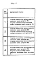
- Fig. 2 In this embodiment, four set point signals shown in Fig. 2 are used. With set point "1" placed in the register 6, the memory 5a is selected by the selection signal 11a if the access signals 10a and 10b come from the microcomputers 1 and 3. With set point "2" placed in the register 6, the memory 5b is selected by the selection signal 11b if the access signals 10a and 10b come from the microcomputers 1 and 3. With set point "3" placed in the register 6, the memory 5a is selected by the output of the selection signal 11a from the register 6 if the access signal 10b comes from the program executing microcomputer 3; if the access signal 10a comes from the program controlling microcomputer 1, the memory 5b is selected by the output of the selection signal 11b from the register 6.
- the memory 5b is selected by the output of the selection signal 11b from the register 6 if the access signal 10b comes from the program executing microcomputer 3; if the access signal 10a comes from the program controlling microcomputer 1, the memory 5a is selected by the output of the selection signal 11a from the register 6.
- Fig. 3 is a view showing an instruction cycle of the program executing microcomputer 3.
- One instruction cycle of the microcomputer 3 comprises an instruction fetch operation "a,” a decode operation “b,” an address computation “c,” an I/O access operation “d,” and execution “e.”
- the sequencer bus 9 is monopolized during the instruction fetch operation "a” and 1/0 access operation "d.”
- the sequencer bus 9 is free. During this bus free period, the program controlling microcomputer 1 may use the sequencer bus 9.
- the programmable controller whose construction was described above works as follows.
- the program controlling microcomputer 1 sets a "1" to the register 6, the program executing microcomputer 3 outputs the access signal 10b to the register 6 and places an address signal onto the sequencer bus 9 in order to read a user program instruction from memory.
- the address signal causes the user program #1 in the memory 5a to be accessed.
- the program executing microcomputer 3 fetches and executes the suitable instruction. If the program controlling microcomputer 1 reads out the user program #1 being executed so as to duplicate it in an external memory, the access signal 10a is output to the register 6 and the address signal is placed on the microcomputer bus 8 in the cycle in which the program executing microcomputer 3 is not using the sequencer bus 9.
- the address signal is placed on the sequencer bus 9 via the bus interface 4. This causes the user program #1 to be read out of the memory 5a. If the user program being executed is stored in the memory 5b, a "2" is set in the register 6, and the subsequence process is the same as described above.
- a "3" is set in the register 6.
- the program executing microcomputer 3 continues reading the user program #1 from the memory 5a for execution, which allows the program controlling microcomputer 1 to access the memory 5b.
- This makes it possible to update the user program #1 that was moved to the external memory as described above and to have the program controlling microcomputer 1 store the updated user program #2 into the memory 5b.
- the updating may be carried out by an external programming device and the updated program may be checked for error thereafter.
- the user program may also be checked by the program controlling microcomputer 1 after being stored into the memory 5b. Where no external programming device is used, the user program #1 may be copied into the memory 5b in which the user program may be updated by the program controlling microcomputer 1. If the user program #2 is to be updated while being executed, a "4" is set in the register 6, and the subsequence process is the same as described above.
- user programs are switched without interruption of the sequence processing.
- the invention also allows the newly selected user program to be verified before its execution.
Landscapes
- Engineering & Computer Science (AREA)
- Software Systems (AREA)
- General Engineering & Computer Science (AREA)
- Theoretical Computer Science (AREA)
- Computer Security & Cryptography (AREA)
- Physics & Mathematics (AREA)
- General Physics & Mathematics (AREA)
- Programmable Controllers (AREA)
Applications Claiming Priority (2)
| Application Number | Priority Date | Filing Date | Title |
|---|---|---|---|
| JP66792/90 | 1990-03-19 | ||
| JP2066792A JP2875842B2 (ja) | 1990-03-19 | 1990-03-19 | プログラマブルコントローラ |
Publications (3)
| Publication Number | Publication Date |
|---|---|
| EP0447685A2 true EP0447685A2 (de) | 1991-09-25 |
| EP0447685A3 EP0447685A3 (en) | 1992-11-19 |
| EP0447685B1 EP0447685B1 (de) | 1999-03-31 |
Family
ID=13326072
Family Applications (1)
| Application Number | Title | Priority Date | Filing Date |
|---|---|---|---|
| EP90125864A Expired - Lifetime EP0447685B1 (de) | 1990-03-19 | 1990-12-31 | Programmierbares Steuergerät |
Country Status (5)
| Country | Link |
|---|---|
| US (1) | US5600807A (de) |
| EP (1) | EP0447685B1 (de) |
| JP (1) | JP2875842B2 (de) |
| DE (1) | DE69033031T2 (de) |
| ES (1) | ES2133268T3 (de) |
Cited By (1)
| Publication number | Priority date | Publication date | Assignee | Title |
|---|---|---|---|---|
| EP0606817A1 (de) * | 1992-12-14 | 1994-07-20 | Carrier Corporation | Methode und Vorrichtung zum Laden eines Steuerprogramms in ein Kälteerzeugungssystem |
Families Citing this family (14)
| Publication number | Priority date | Publication date | Assignee | Title |
|---|---|---|---|---|
| JP2997005B2 (ja) * | 1990-04-12 | 2000-01-11 | キヤノン株式会社 | 出力装置 |
| JP2000339008A (ja) * | 1999-05-27 | 2000-12-08 | Hitachi Ltd | プログラマブルコントローラ |
| US6678274B1 (en) * | 1999-07-30 | 2004-01-13 | Riverstone Networks, Inc. | Method and system for managing forwarding tables |
| US7228538B1 (en) * | 2000-05-02 | 2007-06-05 | International Business Machines Corporation | Method, system, and program for updating firmware to a storage system comprised of multiple controllers |
| JP3594035B2 (ja) * | 2003-03-13 | 2004-11-24 | オムロン株式会社 | 制御装置、cpuユニット、プログラマブルコントローラのユーザプログラム編集方法、及びオンラインエディットされる際のプログラマブルコントローラの処理方法 |
| JP2008077265A (ja) * | 2006-09-20 | 2008-04-03 | Fuji Electric Fa Components & Systems Co Ltd | プログラマブルコントローラのプログラム更新方法 |
| WO2008058101A2 (en) * | 2006-11-07 | 2008-05-15 | Sandisk Corporation | Memory controllers for performing resilient firmware upgrades to a functioning memory |
| US8286156B2 (en) * | 2006-11-07 | 2012-10-09 | Sandisk Technologies Inc. | Methods and apparatus for performing resilient firmware upgrades to a functioning memory |
| US20080109647A1 (en) * | 2006-11-07 | 2008-05-08 | Lee Merrill Gavens | Memory controllers for performing resilient firmware upgrades to a functioning memory |
| US7836347B2 (en) | 2007-10-17 | 2010-11-16 | GE Intelligent Platforms Inc. | Service and diagnostic logic scan apparatus and method |
| US8973124B2 (en) | 2012-04-30 | 2015-03-03 | General Electric Company | Systems and methods for secure operation of an industrial controller |
| JP5906972B2 (ja) * | 2012-07-05 | 2016-04-20 | 富士ゼロックス株式会社 | 画像形成装置および画像読取装置 |
| US9116774B2 (en) | 2013-05-14 | 2015-08-25 | Sandisk Technologies Inc. | Firmware updates for multiple product configurations |
| JP5937637B2 (ja) * | 2014-04-30 | 2016-06-22 | ファナック株式会社 | シーケンスプログラムの切り替え時に、切り替え予告信号を出力する制御装置 |
Family Cites Families (5)
| Publication number | Priority date | Publication date | Assignee | Title |
|---|---|---|---|---|
| US4257095A (en) * | 1978-06-30 | 1981-03-17 | Intel Corporation | System bus arbitration, circuitry and methodology |
| US4257097A (en) * | 1978-12-11 | 1981-03-17 | Bell Telephone Laboratories, Incorporated | Multiprocessor system with demand assignable program paging stores |
| DE3610155A1 (de) * | 1986-03-26 | 1987-10-08 | Joachim Bauer | Mehrprozessorsystem fuer paralleles schreiben und lesen von informationen |
| US5012408A (en) * | 1990-03-15 | 1991-04-30 | Digital Equipment Corporation | Memory array addressing system for computer systems with multiple memory arrays |
| US5144242A (en) * | 1990-08-23 | 1992-09-01 | The Regents Of The University Of California | Continually loadable microcode store for MRI control sequencers |
-
1990
- 1990-03-19 JP JP2066792A patent/JP2875842B2/ja not_active Expired - Lifetime
- 1990-12-31 ES ES90125864T patent/ES2133268T3/es not_active Expired - Lifetime
- 1990-12-31 EP EP90125864A patent/EP0447685B1/de not_active Expired - Lifetime
- 1990-12-31 DE DE69033031T patent/DE69033031T2/de not_active Expired - Lifetime
-
1994
- 1994-04-22 US US08/231,642 patent/US5600807A/en not_active Expired - Lifetime
Cited By (1)
| Publication number | Priority date | Publication date | Assignee | Title |
|---|---|---|---|---|
| EP0606817A1 (de) * | 1992-12-14 | 1994-07-20 | Carrier Corporation | Methode und Vorrichtung zum Laden eines Steuerprogramms in ein Kälteerzeugungssystem |
Also Published As
| Publication number | Publication date |
|---|---|
| ES2133268T3 (es) | 1999-09-16 |
| EP0447685B1 (de) | 1999-03-31 |
| JP2875842B2 (ja) | 1999-03-31 |
| DE69033031D1 (de) | 1999-05-06 |
| JPH03268005A (ja) | 1991-11-28 |
| EP0447685A3 (en) | 1992-11-19 |
| DE69033031T2 (de) | 1999-12-16 |
| US5600807A (en) | 1997-02-04 |
Similar Documents
| Publication | Publication Date | Title |
|---|---|---|
| EP0447685A2 (de) | Programmierbares Steuergerät | |
| JP2526688B2 (ja) | プログラマブルコントロ―ラおよびシ―ケンスプログラムの部分実行方法 | |
| KR960010919B1 (ko) | 데이타 프로세서 | |
| KR100276785B1 (ko) | 전자 장치 | |
| US5799144A (en) | Microcomputer for resolving problems found in a program stored in a ROM | |
| US4807178A (en) | Programmable sequence controller having indirect and direct input/output apparatus | |
| US7203867B2 (en) | Processor system, processor and arithmetic processing method | |
| KR100355630B1 (ko) | 롬 정정 유닛을 구비하는 컴퓨터 시스템 | |
| JP2001256044A (ja) | データ処理装置 | |
| JPS59218569A (ja) | マイクロ・コンピユ−タ | |
| KR960001977B1 (ko) | 프로그램가능 제어기의 제어방법 | |
| JP2573251B2 (ja) | プログラマブルコントローラの送信指定方法 | |
| KR20020029921A (ko) | 정적 기억 장치 내의 마이크로 명령어를 수정하는 방법 및장치 | |
| JPH05282232A (ja) | 装置制御機構 | |
| JPS60126731A (ja) | プログラム制御方法 | |
| JPH0353348A (ja) | マイクロプログラムのデバッグ方式 | |
| JPH02133833A (ja) | インサーキツトエミユレータ制御装置 | |
| JPH04107630A (ja) | 中央処理装置 | |
| JPS595931B2 (ja) | 演算処理システムのアドレス停止方式 | |
| JPH04367902A (ja) | プログラマブルコントローラ | |
| JPH05241853A (ja) | プログラマブルコントローラ | |
| JPS6349846A (ja) | 演算処理装置 | |
| WO1989011685A1 (fr) | Systeme de detection des transitions d'etat d'une unite de commande programmable | |
| JPS6370348A (ja) | プログラムテスト用回路 | |
| JPH01130235A (ja) | マイクロコンピュータ開発支援装置 |
Legal Events
| Date | Code | Title | Description |
|---|---|---|---|
| PUAI | Public reference made under article 153(3) epc to a published international application that has entered the european phase |
Free format text: ORIGINAL CODE: 0009012 |
|
| 17P | Request for examination filed |
Effective date: 19901231 |
|
| AK | Designated contracting states |
Kind code of ref document: A2 Designated state(s): CH DE ES FR IT LI SE |
|
| PUAL | Search report despatched |
Free format text: ORIGINAL CODE: 0009013 |
|
| AK | Designated contracting states |
Kind code of ref document: A3 Designated state(s): CH DE ES FR IT LI SE |
|
| 17Q | First examination report despatched |
Effective date: 19960624 |
|
| GRAG | Despatch of communication of intention to grant |
Free format text: ORIGINAL CODE: EPIDOS AGRA |
|
| GRAG | Despatch of communication of intention to grant |
Free format text: ORIGINAL CODE: EPIDOS AGRA |
|
| GRAG | Despatch of communication of intention to grant |
Free format text: ORIGINAL CODE: EPIDOS AGRA |
|
| GRAH | Despatch of communication of intention to grant a patent |
Free format text: ORIGINAL CODE: EPIDOS IGRA |
|
| GRAH | Despatch of communication of intention to grant a patent |
Free format text: ORIGINAL CODE: EPIDOS IGRA |
|
| GRAA | (expected) grant |
Free format text: ORIGINAL CODE: 0009210 |
|
| AK | Designated contracting states |
Kind code of ref document: B1 Designated state(s): CH DE ES FR IT LI SE |
|
| REG | Reference to a national code |
Ref country code: CH Ref legal event code: EP |
|
| REF | Corresponds to: |
Ref document number: 69033031 Country of ref document: DE Date of ref document: 19990506 |
|
| ET | Fr: translation filed | ||
| REG | Reference to a national code |
Ref country code: ES Ref legal event code: FG2A Ref document number: 2133268 Country of ref document: ES Kind code of ref document: T3 |
|
| PLBE | No opposition filed within time limit |
Free format text: ORIGINAL CODE: 0009261 |
|
| STAA | Information on the status of an ep patent application or granted ep patent |
Free format text: STATUS: NO OPPOSITION FILED WITHIN TIME LIMIT |
|
| 26N | No opposition filed | ||
| REG | Reference to a national code |
Ref country code: CH Ref legal event code: NV Representative=s name: TROESCH SCHEIDEGGER WERNER AG |
|
| PGFP | Annual fee paid to national office [announced via postgrant information from national office to epo] |
Ref country code: SE Payment date: 20090918 Year of fee payment: 20 |
|
| PGFP | Annual fee paid to national office [announced via postgrant information from national office to epo] |
Ref country code: ES Payment date: 20091203 Year of fee payment: 20 Ref country code: CH Payment date: 20091008 Year of fee payment: 20 |
|
| PGFP | Annual fee paid to national office [announced via postgrant information from national office to epo] |
Ref country code: IT Payment date: 20091027 Year of fee payment: 20 Ref country code: FR Payment date: 20091203 Year of fee payment: 20 |
|
| PGFP | Annual fee paid to national office [announced via postgrant information from national office to epo] |
Ref country code: DE Payment date: 20091123 Year of fee payment: 20 |
|
| REG | Reference to a national code |
Ref country code: CH Ref legal event code: PL |
|
| REG | Reference to a national code |
Ref country code: ES Ref legal event code: FD2A Effective date: 20110614 |
|
| PG25 | Lapsed in a contracting state [announced via postgrant information from national office to epo] |
Ref country code: ES Free format text: LAPSE BECAUSE OF EXPIRATION OF PROTECTION Effective date: 20110101 |
|
| PG25 | Lapsed in a contracting state [announced via postgrant information from national office to epo] |
Ref country code: DE Free format text: LAPSE BECAUSE OF EXPIRATION OF PROTECTION Effective date: 20101231 |