EP0448861A1 - Dispositif de circuit intégré semi-conducteur - Google Patents
Dispositif de circuit intégré semi-conducteur Download PDFInfo
- Publication number
- EP0448861A1 EP0448861A1 EP90309030A EP90309030A EP0448861A1 EP 0448861 A1 EP0448861 A1 EP 0448861A1 EP 90309030 A EP90309030 A EP 90309030A EP 90309030 A EP90309030 A EP 90309030A EP 0448861 A1 EP0448861 A1 EP 0448861A1
- Authority
- EP
- European Patent Office
- Prior art keywords
- integrated circuit
- semiconductor integrated
- circuit device
- electromagnetic coil
- circuit substrate
- Prior art date
- Legal status (The legal status is an assumption and is not a legal conclusion. Google has not performed a legal analysis and makes no representation as to the accuracy of the status listed.)
- Granted
Links
- 239000004065 semiconductor Substances 0.000 title claims abstract description 114
- 239000000758 substrate Substances 0.000 claims abstract description 68
- 239000004020 conductor Substances 0.000 claims abstract description 16
- 238000005259 measurement Methods 0.000 claims abstract description 16
- 230000003287 optical effect Effects 0.000 claims description 60
- 238000006073 displacement reaction Methods 0.000 claims description 24
- 230000005389 magnetism Effects 0.000 claims description 3
- 238000005530 etching Methods 0.000 description 12
- 229910052710 silicon Inorganic materials 0.000 description 8
- 239000010703 silicon Substances 0.000 description 8
- XUIMIQQOPSSXEZ-UHFFFAOYSA-N Silicon Chemical compound [Si] XUIMIQQOPSSXEZ-UHFFFAOYSA-N 0.000 description 7
- 239000012530 fluid Substances 0.000 description 7
- 238000005516 engineering process Methods 0.000 description 6
- 230000007246 mechanism Effects 0.000 description 5
- 238000000034 method Methods 0.000 description 5
- VYPSYNLAJGMNEJ-UHFFFAOYSA-N Silicium dioxide Chemical compound O=[Si]=O VYPSYNLAJGMNEJ-UHFFFAOYSA-N 0.000 description 4
- 229910052814 silicon oxide Inorganic materials 0.000 description 4
- ZOXJGFHDIHLPTG-UHFFFAOYSA-N Boron Chemical compound [B] ZOXJGFHDIHLPTG-UHFFFAOYSA-N 0.000 description 2
- 230000015572 biosynthetic process Effects 0.000 description 2
- 229910052796 boron Inorganic materials 0.000 description 2
- 230000004907 flux Effects 0.000 description 2
- 230000001939 inductive effect Effects 0.000 description 2
- 230000000149 penetrating effect Effects 0.000 description 2
- 230000001133 acceleration Effects 0.000 description 1
- 229910052782 aluminium Inorganic materials 0.000 description 1
- XAGFODPZIPBFFR-UHFFFAOYSA-N aluminium Chemical compound [Al] XAGFODPZIPBFFR-UHFFFAOYSA-N 0.000 description 1
- 238000013459 approach Methods 0.000 description 1
- 238000005452 bending Methods 0.000 description 1
- 239000013078 crystal Substances 0.000 description 1
- 238000011161 development Methods 0.000 description 1
- 230000005674 electromagnetic induction Effects 0.000 description 1
- 238000003780 insertion Methods 0.000 description 1
- 230000037431 insertion Effects 0.000 description 1
- 238000004519 manufacturing process Methods 0.000 description 1
- 239000000463 material Substances 0.000 description 1
- 239000011159 matrix material Substances 0.000 description 1
- 229910052751 metal Inorganic materials 0.000 description 1
- 239000002184 metal Substances 0.000 description 1
- 238000009877 rendering Methods 0.000 description 1
Images


Classifications
-
- G—PHYSICS
- G01—MEASURING; TESTING
- G01B—MEASURING LENGTH, THICKNESS OR SIMILAR LINEAR DIMENSIONS; MEASURING ANGLES; MEASURING AREAS; MEASURING IRREGULARITIES OF SURFACES OR CONTOURS
- G01B7/00—Measuring arrangements characterised by the use of electric or magnetic techniques
- G01B7/02—Measuring arrangements characterised by the use of electric or magnetic techniques for measuring length, width or thickness
- G01B7/023—Measuring arrangements characterised by the use of electric or magnetic techniques for measuring length, width or thickness for measuring distance between sensor and object
-
- B—PERFORMING OPERATIONS; TRANSPORTING
- B82—NANOTECHNOLOGY
- B82Y—SPECIFIC USES OR APPLICATIONS OF NANOSTRUCTURES; MEASUREMENT OR ANALYSIS OF NANOSTRUCTURES; MANUFACTURE OR TREATMENT OF NANOSTRUCTURES
- B82Y15/00—Nanotechnology for interacting, sensing or actuating, e.g. quantum dots as markers in protein assays or molecular motors
-
- G—PHYSICS
- G01—MEASURING; TESTING
- G01D—MEASURING NOT SPECIALLY ADAPTED FOR A SPECIFIC VARIABLE; ARRANGEMENTS FOR MEASURING TWO OR MORE VARIABLES NOT COVERED IN A SINGLE OTHER SUBCLASS; TARIFF METERING APPARATUS; MEASURING OR TESTING NOT OTHERWISE PROVIDED FOR
- G01D5/00—Mechanical means for transferring the output of a sensing member; Means for converting the output of a sensing member to another variable where the form or nature of the sensing member does not constrain the means for converting; Transducers not specially adapted for a specific variable
- G01D5/12—Mechanical means for transferring the output of a sensing member; Means for converting the output of a sensing member to another variable where the form or nature of the sensing member does not constrain the means for converting; Transducers not specially adapted for a specific variable using electric or magnetic means
- G01D5/14—Mechanical means for transferring the output of a sensing member; Means for converting the output of a sensing member to another variable where the form or nature of the sensing member does not constrain the means for converting; Transducers not specially adapted for a specific variable using electric or magnetic means influencing the magnitude of a current or voltage
- G01D5/20—Mechanical means for transferring the output of a sensing member; Means for converting the output of a sensing member to another variable where the form or nature of the sensing member does not constrain the means for converting; Transducers not specially adapted for a specific variable using electric or magnetic means influencing the magnitude of a current or voltage by varying inductance, e.g. by a movable armature
- G01D5/2006—Mechanical means for transferring the output of a sensing member; Means for converting the output of a sensing member to another variable where the form or nature of the sensing member does not constrain the means for converting; Transducers not specially adapted for a specific variable using electric or magnetic means influencing the magnitude of a current or voltage by varying inductance, e.g. by a movable armature by influencing the self-induction of one or more coils
- G01D5/2033—Mechanical means for transferring the output of a sensing member; Means for converting the output of a sensing member to another variable where the form or nature of the sensing member does not constrain the means for converting; Transducers not specially adapted for a specific variable using electric or magnetic means influencing the magnitude of a current or voltage by varying inductance, e.g. by a movable armature by influencing the self-induction of one or more coils controlling the saturation of a magnetic circuit by means of a movable element, e.g. a magnet
-
- H—ELECTRICITY
- H01—ELECTRIC ELEMENTS
- H01F—MAGNETS; INDUCTANCES; TRANSFORMERS; SELECTION OF MATERIALS FOR THEIR MAGNETIC PROPERTIES
- H01F7/00—Magnets
- H01F7/06—Electromagnets; Actuators including electromagnets
- H01F7/066—Electromagnets with movable winding
Definitions
- This invention relates to a semiconductor integrated circuit device, and more particularly to a semiconductor actuator utilizing an electromagnetic force, or a semiconductor sensor utilizing an electromagnetic induction.
- optical head of a structure which will be described below will be provided.
- This optical head is composed of, e.g., a cylindrical magnet, a cylindrical bobbin, and a semiconductor chip on which an optical integrated circuit-type pickup is formed.
- the cylindrical bobbin is of a hollow structure in which the diameter of the hollow portion is larger than that of the cylindrical magnet. This cylindrical bobbin is mounted on the cylindrical magnet so that it is seated thereon.
- One end surface of the cylindrical bobbin is closed and the semiconductor chip is affixed on that end surface.
- an electromagnetic coil is provided on the cylindrical side surface of the cylindrical bobbin so as to surround it.
- a magnetic field is formed by magnetic lines of force directed from one end surface of the cylindrical magnet toward the other end surface thereof. These magnetic lines of force penetrate through the end surface of the bobbin and the semiconductor chip surface.
- An object of this invention is to provide a semiconductor integrated circuit device which can be utilized as a small-sized and lightweight actuator or a small-sized sensor.
- an electromagnetic coil is provided on a semiconductor integrated circuit substrate.
- a pair of conductors are drawn out from the magnetic coil.
- the semiconductor integrated circuit substrate is movably arranged within a magnetic field.
- a right-handed magnetic field is produced toward the direction in which the current flows in accordance with "Ampere's right-handed screw rule".
- an attractive force or a repulsive force in a direction of the magnetic lines of force is exerted on the electromagnetic coil.
- the semiconductor integrated circuit substrate also moves in the positive or negative direction of the magnetic lines of force in the direction of the magnetic field. This permits the semiconductor integrated circuit device to operate as a subminiature actuator.
- an optical head for recording/playback of an optical disk which is smaller and lighter than the conventional optical head, can be advantageously provided.
- such a device in the case of moving this semiconductor integrated circuit substrate within a magnetic field, or changing that magnetic field, by measuring an induced current produced in the coil, such a device can be advantageously used as a semiconductor integrated circuit device having a subminiature sensor function for measuring changes in a physical quantity such as displacement, pressure, magnetism, or the like.
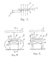
- the conventional optical head is constituted as shown in FIGS. 1 and 2.
- a semiconductor chip 101 on which an optical integrated circuit type pickup is formed is mounted or affixed on a cylindrical bobbin 112.
- An electromagnetic coil 110 is provided on the cylindrical surface of the bobbin 112.
- the bobbin 112 is mounted, in an insertion hole 118, on a cylindrical portion 117 of a lower yoke 116 of a magnet 114 so that it is seated thereon, and is movable in the axial direction of the cylindrical portion 117 (A-A direction).
- a magnetic field exists by the magnet 114.
- a current is caused to flow in the electromagnetic coil 110 through lead wires 111, an electromagnetic force is exerted on the electromagnetic coil 110, so it moves in the A-A direction.
- the electromagnetic coil 110 and the magnet 114 form a focusing actuator.
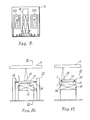
- the basic embodiment of this invention is constituted as shown in FIG. 3.
- this semiconductor integrated circuit device 1 is such that an electromagnetic coil 3 is provided on a semiconductor integrated circuit substrate 2. A pair of conductors 4 are drawn out from the electromagnetic coil 3. Further, the semiconductor integraged circuit substrate 2 is movably disposed within a magnetic field M.
- FIGS. 4 and 5 An optical head which is a first embodiment of a semiconductor integrated circuit device according to this invention is shown in FIGS. 4 and 5.
- This optical head 11 comprises a semiconductor integrated circuit substrate 12, a magnet 15 for producing a magnetic field and a flexible printed wiring board 16 as support means serving as conductors.
- An optical integrated circuit type pickup 18 is formed on the front side 12A of the semiconductor integrated circuit substrate 12, and an electromagnetic coil 13 is formed on the back side 12B thereof.
- the front side 12A opposite to the optical disk D of the semiconductor integrated circuit substrate 12 and the side 12B corresponding to the back side thereof and opposite to the magnet 15 are shown in FIGS. 6 and 7, respectively.
- the optical integrated circuit type pickup 18 comprises a laser diode 18L, a focusing grating coupler 18C, a grating beam splitter 18S, and photo detectors 18D.
- the laser diode 18L generates a laser beam.
- This laser beam is conducted to the focusing grating coupler 18c through an optical waveguide layer (not shown) of the semiconductor integrated circuit substrate 12.
- the focusing grating coupler 18C changes the laser beam so as to take a form of spots by the object lens action to focus it onto information pits on the recording surface of the optical disk D.
- the laser beam is reflected on the surface of the information pits.
- the reflected light is incident back to the focusing grating coupler 18C for a second time, and is then conducted to the grating beam splitter 18S.
- the grating beam splitter 18S splits the reflected light into those in two light paths. These two split light rays are incident to four photo detectors 18D. These photo detectors 18D output electric signals corresponding to a quantity of incident light rays. From these electric signals, information signals and signals for servo control control are provided.
- the electromagnetic coil 13 is provided on the side 12B. Lines of magnetic force based on a magnetic field produced by the magnet 15 penetrate through the electromagnetic coil 13 on the semiconductor integrated circuit substrate 12.
- the flexible printed wiring board 16 is constituted, as shown in FIG. 8, by assembling an elastic member 16S like a metal film for rendering suitable rigidity and elasticity and lead wires 16L of conductors for wiring into a film like matrix 16M having elastic and insulating properties like a plastic material.
- the electrical connection between the lead wires 16L and the optical integrated circuit type pickup 18 or the electromagnetic coil 13 is carried out through land terminals 16T.
- This flexible printed wiring board 16 is constituted, as shown in FIGS. 4 and 5, by bending the both end portions of a belt-shaped flexible printed wiring board to cover the surface of the magnet 15 in a manner to take a form of cylinder or leaf spring. Further, the semiconductor integrated circuit substrate 12 is mounted or affixed on the surface of this flexible printed wiring board 16 just above the magnet 15. Accordingly, the semiconductor integrated circuit substrate 12 is resiliently supported by the flexible printed wiring plate 16. Thus, this substrate can move in the direction of the optical disk D (B-B direction). In this case, the portion of the flexible printed wiring board 16 immediately above the focusing grating coupler 18C of the optical integrated circuit type pickup 18 is cut out in the form of a window as indicated by reference symbol 16W of FIG. 8. Thus, an arrangement such that irradiation of a laser beam is not prevented is provided.
- the method of forming the electromagnetic coil provided on the semiconductor integrated circuit substrate and the configuration of the electromagnetic coil will now be described.
- the electromagnetic coil 13 is formed by using the multilayer interconnection formation technology which is one of integrated circuit technologies to etch a spiral coil pattern on the surface of a silicon substrate to vacuum-deposit aluminum, etc. thereon.
- the pattern of the electromagnetic coil is not limited to a square spiral shown in FIG. 7. Further, patterns of circle, ellipse, or other curves may be used. This coil pattern may be constructed not only in a planar spiral form but also in a three-dimensional spiral or helical form in layer direction in the same manner as in an ordinary electromagnetic coil by the application of the multilayer interconnection technology. In addition, the number of coil patterns on a single semiconductor integrated circuit substrate is not limited to one as in the pattern shown in FIG. 7. Two coil patterns or more may be adopted. For example, as shown in FIG. 9, there may be employed an arrangement to provide two electromagnetic coils 13A and 13B so that the optical integrated circuit type pickup 18 is put therebetween.
- the electromagnetic coil may be provided on either side of the semiconductor integrated circuit substrate 12.
- FIGS. 10 and 11 An optical head which is a second embodiment of a semiconductor integrated circuit device according to this invention is shown in FIGS. 10 and 11.
- This optical head 21 differs from the optical head 11 in the first embodiment in that four elastic supporters 26 are affixed on the semiconductor integrated circuit substrate 12 as support means in place of the flexible printed wiring board 16 of the optical head 11 in the first embodiment shown in FIGS. 4 to 9.
- These supporters 26 may be not only in the form of coil, rod and plate, etc., but also in other forms.
- the number of supporters is not limited to four as in the embodiment.
- the electromagnetic coil is provided on the semiconductor integrated circuit substrate provided with the optical integrated circuit type pickup, thus to allow the semiconductor integrated circuit device to have a function as the optical head.
- this invention is not limited to the optical integrated circuit type pickup, but can be utilized as a semiconductor integrated circuit device where another integrated circuit is mounted on a semiconductor integrated circuit substrate and the semiconductor integrated circuit substrate itself can be moved.
- the device of this invention may be used as a miniaturized actuator including no integrated circuit and directed to only drive.
- a displacement sensor which is a third embodiment of a semiconductor integrated circuit device according to this invention is shown in FIG. 12.
- This displacement sensor 31 is constituted of a structure such that the optical integrated circuit type pickup is removed from the optical head 11 of the first embodiment shown in FIGS. 4 to 9, and that a rod 37 for allowing the semiconductor integrated circuit substrate to interlock with a measurement object is instead provided so that it comes in contact with that substrate.
- the semiconductor integrated circuit substrate 12 indicates a quantity of displacement equal to a quantity of displacement in the C-C direction of the end point 37A of the rod 37.
- an induced current corresponding to a displacement velocity of the semiconductor integrated circuit substrate 12 flows in the electromagnetic coil 13. Accordingly, by measuring such an induced current by a galvanometer, etc. through conductors (not shown), velocity, position, and acceleration, etc. can be calculated.
- the mechanism for allowing the substrate to interlock with a measurement object is not limited to the rod, but may be other mechanisms.
- a displacement sensor of a structure such that the optical integrated circuit type pickup is removed from the second embodiment of FIGS. 10 and 11, and a rod 37 of the interlocking means is instead provided so that it comes in contact with the semiconductor integrated circuit substrate is also effective as a fourth embodiment of this invention.
- FIG. 14 The cross section of a pressure sensor which is a fifth embodiment of a semiconductor integrated circuit device according to this invention is shown in FIG. 14.
- This pressure sensor 50 comprises a pressure vessel 51 for containing fluid for measuring pressure, and a semiconductor integrated circuit substrate 52.
- the semiconductor integrated circuit substrate 52 is affixed, on the pressure vessel 51, on a diaphragm 57 serving as the support means and for allowing the substrate to interlock with a measurement object, and the semiconductor integrated circuit substrate 52 includes an electromagnetic coil 53. Further, a magnet 55 for producing a magnetic field is provided immediately above the semiconductor integrated circuit substrate 52.
- the fluid L is conducted into the pressure vessel 51 through a pouring tube 58.
- a displacement sensor which is a sixth embodiment of a semiconductor integrated circuit device according to this invention is shown in FIG. 15.
- This displacement sensor 61 comprises a semiconductor integrated circuit substrate 62, a magnet 65 for producing a magnetic field, a rod 67 for allowing the substrate 62 to interlock with a measurement object, and a support 68.
- the magnet 65 is provided immediately above the semiconductor integrated circuit substrate 62. Further, a cantilever member 66 is formed on the semiconductor integrated circuit substrate 62. An electromagnetic coil 63 is provided on the cantilever member 66. In this embodiment, the cantilever member 66 constitutes the support means.
- the rod 67 is in contact with the cantilever member 66 to transmit a displacement in the E-E direction of an end point 67A to the cantilever member 66 by the support 68.
- this displacement sensor 61 has, in the same manner as in the displacement sensor shown in FIGS. 12 and 13, a sensor function to respond to a displacement given to the terminal point 67A of the rod 67 to convert a quantity of that displacement to an electric output to output it.
- the support means is incorporated as the cantilever member into the semiconductor integrated circuit substrate.
- the displacement sensor of this embodiment can be advantageously smaller than the displacement sensors of the third and fourth embodiments shown in FIGS. 12 and 13. It is to be noted that the mechanism for allowing the substrate to interlock with a measurement object is not limited to the rod, but may be other mechanisms.
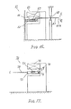
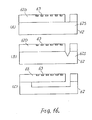
- FIG. 16 A method of forming the cantilever member 66 of the semiconductor integrated circuit substrate 62 is shown in FIG. 16.
- a silicon oxide film 62D is formed on a silicon substrate 62S.
- An electromagnetic coil 63 is then formed by the multilayer interconnection formation technology.
- the silicon oxide film 62D is etched (FIG. 16(A)).
- the exposed silicon surface is etched by the anisotropy etching of which the each rate varies in dependence upon the direction of the crystal. In the beginning, etching proceeds so that a V-shaped groove is formed (FIG. 16(B)).
- cantilever member 66 including electromagnetic coil 63 on the surface thereof can be formed (FIG. 16 (C)).
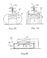
- a pressure sensor which is a seventh embodiment of a semiconductor integrated circuit device according to this invention is shown in FIG. 17.
- This pressure sensor 70 comprises a semiconductor pressure vessel 71, and a magnet 75 for producing a magnetic field provided immediately above the semiconductor pressure vessel 71.
- a diaphragm 76 is provided in the semiconductor pressure vessel 71.
- An electromagnetic coil 73 is provided on the diaphragm 76.
- fluid L for measuring a pressure is conducted into the semiconductor pressure vessel 71 through a pouring tube 78 communicating with the semiconductor pressure vessel 71.
- the diaphragm 76 allows the semiconductor integrated circuit substrate to interlock with a measurement object.
- FIG. 18 A method of forming this semiconductor pressure vessel 71 is shown in FIG. 18.
- an etching stop portion 72B for stopping etching is formed.
- electromagnetic coil 73 is formed by the multilayer interconnection technology within the portion surrounded by the etching stop portion 72B (FIG. 18(A)).
- etching is applied to the bellows portion of the diaphragm around the electromagnetic coil 73 on the surface of the silicon substrate 72S (FIG. 18(B)).
- etching stop layer 76B (FIG. 18(C)).
- semiconductor pressure vessel 71 can be formed (FIG. 18(E)).
- the configurations and the numbers of the coil patterns in the above-described third to seventh embodiments are not limited to those mentioned therein, but may be other configurations and numbers.
- sensors in the above-described third to seventh embodiments can measure not only so called mechanical changes in the physical quantity such as displacement, velocity and the like, but also changes in the magnetism. Namely, when an external magnetic field changes, for example, when an object producing a magnetic filed comes into contact with the sensor and is away from therefrom, or the like, it is also possible to measure changes in a magnetic filed by measuring an inductive current which is caued to flow by the mutual inductive action of the electromagnetic coil.
- the magnet for producing a magnetic field may be a permanent magnet or an electromagnet.
- the semiconductor integrated circuit device of this invention can be applied not only as a semiconductor integrated circuit device having an actuator function and a semiconductor integrated circuit device having a sensor function, but also as a semiconductor integrated circuit device having an actuator function and a sensor function combined with each other.
- an approach may be also employed to further provide a velocity coil for detecting a velocity of the optical head on the semiconductor integrated circuit substrate 12 to constitute a miniaturized optical head having a function to detect a velocity at the time of track jump motion.
Landscapes
- Physics & Mathematics (AREA)
- Engineering & Computer Science (AREA)
- General Physics & Mathematics (AREA)
- Electromagnetism (AREA)
- Nanotechnology (AREA)
- Chemical & Material Sciences (AREA)
- Molecular Biology (AREA)
- General Health & Medical Sciences (AREA)
- Crystallography & Structural Chemistry (AREA)
- Life Sciences & Earth Sciences (AREA)
- Health & Medical Sciences (AREA)
- Power Engineering (AREA)
- Optical Recording Or Reproduction (AREA)
- Micromachines (AREA)
- Optical Head (AREA)
Applications Claiming Priority (2)
| Application Number | Priority Date | Filing Date | Title |
|---|---|---|---|
| JP67885/90 | 1990-03-16 | ||
| JP2067885A JP2768792B2 (ja) | 1990-03-16 | 1990-03-16 | 半導体集積回路装置 |
Publications (2)
| Publication Number | Publication Date |
|---|---|
| EP0448861A1 true EP0448861A1 (fr) | 1991-10-02 |
| EP0448861B1 EP0448861B1 (fr) | 1994-10-19 |
Family
ID=13357803
Family Applications (1)
| Application Number | Title | Priority Date | Filing Date |
|---|---|---|---|
| EP90309030A Expired - Lifetime EP0448861B1 (fr) | 1990-03-16 | 1990-08-17 | Dispositif de circuit intégré semi-conducteur |
Country Status (4)
| Country | Link |
|---|---|
| US (1) | US5631488A (fr) |
| EP (1) | EP0448861B1 (fr) |
| JP (1) | JP2768792B2 (fr) |
| DE (1) | DE69013491T2 (fr) |
Cited By (1)
| Publication number | Priority date | Publication date | Assignee | Title |
|---|---|---|---|---|
| EP0816861A3 (fr) * | 1996-06-25 | 2000-03-29 | Siemens Aktiengesellschaft | Dispositif de mesure de champs magnétiques |
Families Citing this family (4)
| Publication number | Priority date | Publication date | Assignee | Title |
|---|---|---|---|---|
| JP3318486B2 (ja) * | 1996-06-14 | 2002-08-26 | アルプス電気株式会社 | 熱転写プリンタ |
| LV12835B (en) | 2000-11-24 | 2002-07-20 | Leon�ds BE�ERS | Micromovement measuring device and a method of displacement-to-signal conversion embodied in said device |
| DE102004047188B4 (de) | 2004-09-29 | 2022-10-27 | Robert Bosch Gmbh | Vorrichtung zur Ortung metallischer Objekte |
| DE102010041214A1 (de) * | 2010-09-22 | 2012-03-22 | Siemens Aktiengesellschaft | Schaltgerät sowie Verfahren zur Steuerung eines Schaltgeräts |
Citations (4)
| Publication number | Priority date | Publication date | Assignee | Title |
|---|---|---|---|---|
| US3699249A (en) * | 1962-02-28 | 1972-10-17 | Magnavox Co | Facsimile systems, transceivers, and marking transducers therefor |
| DE2701296B1 (de) * | 1977-01-14 | 1978-04-20 | Philips Patentverwaltung | Duennschicht-Magnetfeld-Sensor |
| GB2200461A (en) * | 1987-01-27 | 1988-08-03 | Ford Motor Co | Noncontacting position and pick-up sensor |
| US4779259A (en) * | 1985-04-25 | 1988-10-18 | Mitsubishi Denki Kabushiki Kaisha | Optical head assembly with efficient light source coupling surface and method of construction |
Family Cites Families (8)
| Publication number | Priority date | Publication date | Assignee | Title |
|---|---|---|---|---|
| US3258723A (en) * | 1962-01-30 | 1966-06-28 | Osafune ia | |
| US3533022A (en) * | 1967-08-11 | 1970-10-06 | Gen Electric | Magnetically driven electromechanical filter with cantilevered resonator and variable q |
| US3671793A (en) * | 1969-09-16 | 1972-06-20 | Itt | High frequency transistor structure having an impedance transforming network incorporated on the semiconductor chip |
| FR2582136B1 (fr) * | 1985-05-14 | 1987-06-26 | Labo Electronique Physique | Dispositif a transfert de charges muni d'organes selfiques |
| JPS635307A (ja) * | 1986-06-25 | 1988-01-11 | Matsushita Electric Ind Co Ltd | 光導波装置 |
| JPH0675294B2 (ja) * | 1987-08-25 | 1994-09-21 | 東京電気株式会社 | 対物レンズ駆動装置 |
| JP2614455B2 (ja) * | 1987-08-31 | 1997-05-28 | 日本電気ホームエレクトロニクス株式会社 | 光ヘッドの対物レンズアクチュエータ |
| JPH01154522U (fr) * | 1988-04-14 | 1989-10-24 |
-
1990
- 1990-03-16 JP JP2067885A patent/JP2768792B2/ja not_active Expired - Fee Related
- 1990-08-17 DE DE69013491T patent/DE69013491T2/de not_active Expired - Fee Related
- 1990-08-17 EP EP90309030A patent/EP0448861B1/fr not_active Expired - Lifetime
-
1992
- 1992-03-23 US US07/855,496 patent/US5631488A/en not_active Expired - Fee Related
Patent Citations (4)
| Publication number | Priority date | Publication date | Assignee | Title |
|---|---|---|---|---|
| US3699249A (en) * | 1962-02-28 | 1972-10-17 | Magnavox Co | Facsimile systems, transceivers, and marking transducers therefor |
| DE2701296B1 (de) * | 1977-01-14 | 1978-04-20 | Philips Patentverwaltung | Duennschicht-Magnetfeld-Sensor |
| US4779259A (en) * | 1985-04-25 | 1988-10-18 | Mitsubishi Denki Kabushiki Kaisha | Optical head assembly with efficient light source coupling surface and method of construction |
| GB2200461A (en) * | 1987-01-27 | 1988-08-03 | Ford Motor Co | Noncontacting position and pick-up sensor |
Non-Patent Citations (1)
| Title |
|---|
| PATENT ABSTRACTS OF JAPAN vol. 133, no. 8 (P-281) 20 June 1984, & JP-A-59 034127 (YOKOGAWA HOKUSHIN DENKI KK) 24 February 1984, * |
Cited By (1)
| Publication number | Priority date | Publication date | Assignee | Title |
|---|---|---|---|---|
| EP0816861A3 (fr) * | 1996-06-25 | 2000-03-29 | Siemens Aktiengesellschaft | Dispositif de mesure de champs magnétiques |
Also Published As
| Publication number | Publication date |
|---|---|
| JP2768792B2 (ja) | 1998-06-25 |
| US5631488A (en) | 1997-05-20 |
| EP0448861B1 (fr) | 1994-10-19 |
| JPH03268235A (ja) | 1991-11-28 |
| DE69013491T2 (de) | 1995-05-18 |
| DE69013491D1 (de) | 1994-11-24 |
Similar Documents
| Publication | Publication Date | Title |
|---|---|---|
| JPH01125734A (ja) | 光学的読取りヘッドの移動装置 | |
| GB2052829A (en) | Apparatus for driving objective lens in tracking direction | |
| JP3411603B2 (ja) | 光学式情報記録再生装置の対物レンズ電磁駆動装置 | |
| JPH03156711A (ja) | 情報を磁気媒体に書込むための磁気ヘッド及び方法 | |
| EP0121857B1 (fr) | Dispositif de fixation et appareil de commande propre à un appareil de reproduction ou d'enregistrement de disques optiques et appareil de reproduction ou d'enregistrement comportant un tel dispositif ou un tel appareil | |
| US6947228B2 (en) | Objective lens driving device, optical pickup device, and optical information recording and/or reproduction device | |
| JPS6339980B2 (fr) | ||
| JPS6118261B2 (fr) | ||
| JPH0696458A (ja) | 光学式情報記録再生装置の対物レンズ電磁駆動装置 | |
| US5631488A (en) | Semiconductor integrated circuit device | |
| JP2002505790A (ja) | コンパクトなアクチュエータを有するレンズシステムからなる光学走査装置 | |
| US5867468A (en) | Optical pickup with a vertically movable aperture means | |
| US7199949B2 (en) | Optical pickup device and optical disk device | |
| JP2000011408A (ja) | ディスクプレーヤのピックアップ装置 | |
| JPS6098531A (ja) | 光学式情報処理装置 | |
| JP3570838B2 (ja) | 対物レンズ駆動装置 | |
| JP2001273656A (ja) | 光ピックアップの対物レンズ駆動装置 | |
| JPH03217806A (ja) | レンズ位置検出装置 | |
| JPH05250708A (ja) | 光学式情報記録再生装置 | |
| JP2007317259A (ja) | ハードディスク装置 | |
| JP2897090B2 (ja) | 対物レンズ駆動装置 | |
| JPH01220235A (ja) | 光ピックアップ | |
| KR20040108266A (ko) | 초점 심도 조절용 마이크로 액츄에이터 | |
| JP5801582B2 (ja) | ヘッドジンバルアセンブリ、ヘッドジンバルアセンブリの製造方法及びヘッドジンバルアセンブリの製造装置 | |
| KR200235189Y1 (ko) | 광픽업액츄에이터의보빈어셈블리구조 |
Legal Events
| Date | Code | Title | Description |
|---|---|---|---|
| PUAI | Public reference made under article 153(3) epc to a published international application that has entered the european phase |
Free format text: ORIGINAL CODE: 0009012 |
|
| AK | Designated contracting states |
Kind code of ref document: A1 Designated state(s): DE FR GB |
|
| 17P | Request for examination filed |
Effective date: 19911223 |
|
| 17Q | First examination report despatched |
Effective date: 19930413 |
|
| GRAA | (expected) grant |
Free format text: ORIGINAL CODE: 0009210 |
|
| AK | Designated contracting states |
Kind code of ref document: B1 Designated state(s): DE FR GB |
|
| REF | Corresponds to: |
Ref document number: 69013491 Country of ref document: DE Date of ref document: 19941124 |
|
| ET | Fr: translation filed | ||
| REG | Reference to a national code |
Ref country code: GB Ref legal event code: 746 Effective date: 19950421 |
|
| PLBE | No opposition filed within time limit |
Free format text: ORIGINAL CODE: 0009261 |
|
| STAA | Information on the status of an ep patent application or granted ep patent |
Free format text: STATUS: NO OPPOSITION FILED WITHIN TIME LIMIT |
|
| REG | Reference to a national code |
Ref country code: FR Ref legal event code: D6 |
|
| 26N | No opposition filed | ||
| REG | Reference to a national code |
Ref country code: GB Ref legal event code: IF02 |
|
| PGFP | Annual fee paid to national office [announced via postgrant information from national office to epo] |
Ref country code: FR Payment date: 20060808 Year of fee payment: 17 |
|
| PGFP | Annual fee paid to national office [announced via postgrant information from national office to epo] |
Ref country code: DE Payment date: 20060810 Year of fee payment: 17 |
|
| PGFP | Annual fee paid to national office [announced via postgrant information from national office to epo] |
Ref country code: GB Payment date: 20060816 Year of fee payment: 17 |
|
| GBPC | Gb: european patent ceased through non-payment of renewal fee |
Effective date: 20070817 |
|
| REG | Reference to a national code |
Ref country code: FR Ref legal event code: ST Effective date: 20080430 |
|
| PG25 | Lapsed in a contracting state [announced via postgrant information from national office to epo] |
Ref country code: DE Free format text: LAPSE BECAUSE OF NON-PAYMENT OF DUE FEES Effective date: 20080301 |
|
| PG25 | Lapsed in a contracting state [announced via postgrant information from national office to epo] |
Ref country code: FR Free format text: LAPSE BECAUSE OF NON-PAYMENT OF DUE FEES Effective date: 20070831 |
|
| PG25 | Lapsed in a contracting state [announced via postgrant information from national office to epo] |
Ref country code: GB Free format text: LAPSE BECAUSE OF NON-PAYMENT OF DUE FEES Effective date: 20070817 |