EP0454470A2 - Méthode et dispositif de commande d'un appareil d'affichage - Google Patents
Méthode et dispositif de commande d'un appareil d'affichage Download PDFInfo
- Publication number
- EP0454470A2 EP0454470A2 EP91303767A EP91303767A EP0454470A2 EP 0454470 A2 EP0454470 A2 EP 0454470A2 EP 91303767 A EP91303767 A EP 91303767A EP 91303767 A EP91303767 A EP 91303767A EP 0454470 A2 EP0454470 A2 EP 0454470A2
- Authority
- EP
- European Patent Office
- Prior art keywords
- voltage
- scanning
- data
- electrodes
- driving
- Prior art date
- Legal status (The legal status is an assumption and is not a legal conclusion. Google has not performed a legal analysis and makes no representation as to the accuracy of the status listed.)
- Withdrawn
Links
- 238000000034 method Methods 0.000 title claims description 38
- 239000010409 thin film Substances 0.000 description 27
- 238000010586 diagram Methods 0.000 description 9
- 229910052581 Si3N4 Inorganic materials 0.000 description 2
- 229910010252 TiO3 Inorganic materials 0.000 description 2
- PNEYBMLMFCGWSK-UHFFFAOYSA-N aluminium oxide Inorganic materials [O-2].[O-2].[O-2].[Al+3].[Al+3] PNEYBMLMFCGWSK-UHFFFAOYSA-N 0.000 description 2
- 238000010276 construction Methods 0.000 description 2
- 229910052593 corundum Inorganic materials 0.000 description 2
- 238000007599 discharging Methods 0.000 description 2
- 239000011159 matrix material Substances 0.000 description 2
- 230000000630 rising effect Effects 0.000 description 2
- 229910001845 yogo sapphire Inorganic materials 0.000 description 2
- RUDFQVOCFDJEEF-UHFFFAOYSA-N yttrium(III) oxide Inorganic materials [O-2].[O-2].[O-2].[Y+3].[Y+3] RUDFQVOCFDJEEF-UHFFFAOYSA-N 0.000 description 2
- 230000003213 activating effect Effects 0.000 description 1
- 230000005540 biological transmission Effects 0.000 description 1
- 238000006243 chemical reaction Methods 0.000 description 1
- 239000003795 chemical substances by application Substances 0.000 description 1
- 230000000295 complement effect Effects 0.000 description 1
- 238000005401 electroluminescence Methods 0.000 description 1
- 230000008020 evaporation Effects 0.000 description 1
- 238000001704 evaporation Methods 0.000 description 1
- 239000011521 glass Substances 0.000 description 1
- PJXISJQVUVHSOJ-UHFFFAOYSA-N indium(III) oxide Inorganic materials [O-2].[O-2].[O-2].[In+3].[In+3] PJXISJQVUVHSOJ-UHFFFAOYSA-N 0.000 description 1
- 238000009413 insulation Methods 0.000 description 1
- 239000000463 material Substances 0.000 description 1
- 229910044991 metal oxide Inorganic materials 0.000 description 1
- 150000004706 metal oxides Chemical class 0.000 description 1
- 238000012856 packing Methods 0.000 description 1
- 239000004065 semiconductor Substances 0.000 description 1
- 238000004544 sputter deposition Methods 0.000 description 1
- 239000000758 substrate Substances 0.000 description 1
Images


Classifications
-
- G—PHYSICS
- G09—EDUCATION; CRYPTOGRAPHY; DISPLAY; ADVERTISING; SEALS
- G09G—ARRANGEMENTS OR CIRCUITS FOR CONTROL OF INDICATING DEVICES USING STATIC MEANS TO PRESENT VARIABLE INFORMATION
- G09G3/00—Control arrangements or circuits, of interest only in connection with visual indicators other than cathode-ray tubes
- G09G3/20—Control arrangements or circuits, of interest only in connection with visual indicators other than cathode-ray tubes for presentation of an assembly of a number of characters, e.g. a page, by composing the assembly by combination of individual elements arranged in a matrix no fixed position being assigned to or needed to be assigned to the individual characters or partial characters
- G09G3/22—Control arrangements or circuits, of interest only in connection with visual indicators other than cathode-ray tubes for presentation of an assembly of a number of characters, e.g. a page, by composing the assembly by combination of individual elements arranged in a matrix no fixed position being assigned to or needed to be assigned to the individual characters or partial characters using controlled light sources
- G09G3/30—Control arrangements or circuits, of interest only in connection with visual indicators other than cathode-ray tubes for presentation of an assembly of a number of characters, e.g. a page, by composing the assembly by combination of individual elements arranged in a matrix no fixed position being assigned to or needed to be assigned to the individual characters or partial characters using controlled light sources using electroluminescent panels
-
- G—PHYSICS
- G09—EDUCATION; CRYPTOGRAPHY; DISPLAY; ADVERTISING; SEALS
- G09G—ARRANGEMENTS OR CIRCUITS FOR CONTROL OF INDICATING DEVICES USING STATIC MEANS TO PRESENT VARIABLE INFORMATION
- G09G2310/00—Command of the display device
- G09G2310/02—Addressing, scanning or driving the display screen or processing steps related thereto
- G09G2310/0264—Details of driving circuits
- G09G2310/0267—Details of drivers for scan electrodes, other than drivers for liquid crystal, plasma or OLED displays
-
- G—PHYSICS
- G09—EDUCATION; CRYPTOGRAPHY; DISPLAY; ADVERTISING; SEALS
- G09G—ARRANGEMENTS OR CIRCUITS FOR CONTROL OF INDICATING DEVICES USING STATIC MEANS TO PRESENT VARIABLE INFORMATION
- G09G2310/00—Command of the display device
- G09G2310/02—Addressing, scanning or driving the display screen or processing steps related thereto
- G09G2310/0264—Details of driving circuits
- G09G2310/0275—Details of drivers for data electrodes, other than drivers for liquid crystal, plasma or OLED displays, not related to handling digital grey scale data or to communication of data to the pixels by means of a current
-
- G—PHYSICS
- G09—EDUCATION; CRYPTOGRAPHY; DISPLAY; ADVERTISING; SEALS
- G09G—ARRANGEMENTS OR CIRCUITS FOR CONTROL OF INDICATING DEVICES USING STATIC MEANS TO PRESENT VARIABLE INFORMATION
- G09G2310/00—Command of the display device
- G09G2310/02—Addressing, scanning or driving the display screen or processing steps related thereto
- G09G2310/0264—Details of driving circuits
- G09G2310/0281—Arrangement of scan or data electrode driver circuits at the periphery of a panel not inherent to a split matrix structure
Definitions
- the present invention relates to a driving method and a driving device for a display device such as an electroluminescence (abbreviated as EL) display device or other AC driven capacitive flat matrix display panel (hereinafter referred to as the "thin-film EL display device").
- a display device such as an electroluminescence (abbreviated as EL) display device or other AC driven capacitive flat matrix display panel (hereinafter referred to as the "thin-film EL display device”).
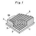
- a double insulation (or three-layered) thin-film EL element is constructed in the following manner.
- strips of transparent electrodes 2 composed of In2O3 are formed parallel to one another on a glass substrate 1.
- an EL layer 4 composed of ZnS or other material doped with an activating agent such as Mn and another dielectric layer 3a composed of Y2O3, Si3N4, TiO3, or Al2O3, each layer having a thickness of 500 to 1,000 ⁇ , are deposited one on top of another above the transparent electrodes 2 using a thin-film technique such as evaporation or sputtering, to form a three-layered construction.
- strips of counter electrodes 5 composed of Al are formed parallel to one another, and at right angles to the transparent electrodes 2, on top of the three-layered construction.
- the thus constructed thin-film EL element can be considered as a capacitive element in terms of circuit equivalence since the EL layer 4 sandwiched between the dielectric layers 3 and 3a is interposed between the electrodes.
- the thin-film EL element is driven by a relatively high voltage on the order of 200 V.
- either the transparent electrodes 2 or the counter electrodes 5 of the thin-film EL element are configured as the scanning-side electrodes and the other as the data-side electrodes, the driving of the display being performed in such a way that a write voltage is applied to the line-sequentially selected scanning-side electrodes by a scanning-side driving circuit consisting of n-channel high voltage MOS (Metal Oxide Semiconductor) driver ICs (integrated circuits) and p-channel high voltage MOS driver ICs, while applying a modulated voltage, which determines emission or non-emission of light according to the display data, to the data-side electrodes by a data-side driving circuit consisting of n-channel high voltage MOS driver ICs and p-channel high voltage MOS driver ICs.
- MOS Metal Oxide Semiconductor
- an AC driving method is employed in which the p-channel driving to apply a write voltage of positive polarity and the n-channel driving to apply a write voltage of negative polarity to the scanning-side electrodes with respect to the ground potential such as the chassis are alternately performed for every frame.
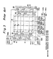
- Fig.3 is a circuit diagram showing an example of the configuration of a thin-film display device in which the prior art driving method is employed.
- Vw emitting threshold voltage
- Scanning-side n-channel high voltage MOS driver ICs 20, 30 and scanning-side p-channel high voltage MOS driver ICs 40, 50 are the circuits constituting the above-mentioned scanning-side driving circuit.
- a data-side driver IC 160 is the circuit that constitutes the above-mentioned data-side driving circuit.
- a data inverting circuit 100 is a circuit comprising an exclusive OR gate, etc. for inverting a data signal DATA, which is input to the data-side driver IC 160, in response to a control signal RVC1.
- the voltage Vm is set at 60V.
- Fig.2 the voltages Vw, (Vw+ 1 2 Vm), and (Vw- 1 2 Vm) are marked alongside of the corresponding voltage values on the x-axis along which the applied voltage is plotted.
- the display device shown is driven in response to externally supplied two synchronizing signals, a vertical synchronizing signal V and a horizontal synchronizing signal H. That is, the p-channel or the n-channel driving is performed on the scanning-side electrodes in line sequential fashion in synchronism with the horizontal synchronizing signal H, and one frame is formed when the line sequential driving of all the scanning electrodes is completed.
- the vertical synchronizing signal V usually indicates the beginning of one frame, and in synchronism with this signal, the driving for one frame is initiated.
- Each scanning-side electrode is subjected in line sequential fashion to the p-channel or the n-channel driving once during one frame period.
- the EL display element 10 requires the applied voltage to alternate, and the p-channel driving and the n-channel driving are performed alternately in such a way that the alternating current cycle is closed with two frames for every scanning-side electrode.
- a method field inversion driving
- line inversion driving in which the driving is performed by inverting the polarity for every scanning line.
- the thin-film EL element is a capacitive element as described earlier, a modulating voltage of 0V or Vm according to the display data is applied to all the data-side electrodes X, repeating charge and discharge every time each scanning-side electrode Y is selectively driven in line sequential fashion; therefore, the thin-film EL element has the problem of consuming a large amount of modulation power.
- the transistors PT2-PTi and NT2-NTi for the remaining scanning-side electrodes Y2-Yi are turned off, and consequently, the remaining scanning-side electrodes Y2-Yi are placed in the so-called floating state. Therefore, the display power P associated with the capacitance C at the scanning-side electrode Y1 to which the write voltage is applied is relatively small.
- the modulated voltage 0 V or Vm is constantly applied to the data-side electrodes X, as described earlier, resulting in a large modulation power Pm because of the capacitance C between all the data-side electrodes X and all the scanning-side electrodes Y. Therefore, reduction in the modulation power Pm is effective for reducing the display power for the entire display device.
- the invention provides a driving method for a display having a plurality of scanning-side electrodes extending in one direction, a plurality of data-side electrodes extending in a second direction intersecting the first direction, and dielectric layers interposed therebetween, picture elements being formed at intersections of the scanning-side electrodes and data-side electrodes, the picture elements being driven by applying a modulated voltage, the magnitude thereof being varied according to the emission or non-emission of light, to the data-side electrodes, while applying a write voltage in line sequential fashion to the scanning-side electrodes, so that a voltage exceeding the emitting threshold voltage of the picture element is applied thereto for emission of light and a voltage below the emitting threshold voltage is applied for non-emission of light, the method comprising: reversing the polarity of the voltage applied between the data-side electrode and the scanning-side electrode corresponding to the picture element to be driven for light emission, one or more times during the period in which the write voltage is being applied to the scanning-side electrode.
- the display device such as an EL panel has a plurality of scanning-side electrodes and a plurality of data-side electrodes arranged intersecting each other in a matrix form with dielectric layers interposed therebetween; a modulated voltage is applied to the data-side electrodes, a write voltage is applied in line sequential fashion to the scanning-side electrodes, and a prescribed voltage exceeding the emitting threshold voltage is applied to the intersection of the data-side electrode and the scanning-side electrode corresponding to the picture element to be driven for light emission.
- the polarity of the voltage applied between the data-side electrode and the scanning-side electrode corresponding to the picture element to be driven for light emission is reversed one or more times.
- the polarity of the voltage applied between the data-side electrode and the scanning-side electrode corresponding to the picture element to be driven for light emission is reversed one or more times during the period in which the write voltage is being applied to the scanning-side electrodes, the desired brightness of light emission can be provided even when the modulated voltage or the write voltage is reduced, or in the case of not reducing the modulated voltage or the write voltage, it is possible to further enhance the brightness of light emission.
- a modulated voltage is applied to the data-side electrodes, a write voltage is applied in line sequential fashion to the scanning-side electrodes, and a voltage exceeding the emitting threshold voltage is applied to the intersection of the data-side electrode and the scanning-side electrode at which the picture element to be driven for light emission is formed, the polarity of the voltage applied between the data-side electrode and the scanning-side electrode corresponding to the picture element to be driven for light emission being reversed one or more times during the period in which the write voltage is being applied to the scanning-side electrode.
- This serves to reduce the modulated voltage Vm and achieve a reduction in the modulation power, which allows the use of a low voltage circuit for the data-side driving circuit for reduction of costs.
- the reduction in the modulation power permits a higher packing density of the data-side driving circuit constructed with integrated circuits, which contributes to the reduction in the size of the display device.
- the polarity of the voltage applied between the data-side electrode and the scanning-side electrode corresponding to the picture element to be driven for light emission is reversed one or more times, it is possible to obtain high brightness even when the modulated voltage or the write voltage is reduced.
- the invention also provides a driving device for a display device having a plurality of scanning-side electrodes, a plurality of data-side electrodes, and dielectric layers interposed therebetween, picture elements being formed at intersections of the scanning-side electrodes and data-side electrodes, comprising: scanning-side electrode driving means connected to the plurality of scanning-side electrodes for applying a positive or negative polarity write voltage to the scanning-side electrodes; data-side electrode driving means connected to the plurality of data-side electrodes, which, when a picture element on the scanning-side electrode supplied with the write voltage is to be driven for light emission, applies a voltage, which cooperates with each write voltage to set a voltage applied to picture element above a threshold voltage, to the corresponding data-side electrode, and when the picture element is not driven for light emission, applies a voltage, which cooperates with each write voltage to set a voltage applied to picture element below a threshold voltage, to the corresponding data-side electrode; and display control means for controlling the scanning-side electrode driving means and the data-side electrode driving
- the invention is characterized in that the scanning-side electrode driving means comprises: odd-numbered electrode driving circuits for applying the write voltage to the odd-numbered scanning-side electrodes; and even-numbered electrode driving circuits for applying the write voltage to the even-numbered scanning-side electrodes.
- the scanning-side electrode driving means comprises: a first potential switching circuit for switching the voltage applied to the odd-numbered and even-numbered electrode driving circuits between a voltage of positive polarity and a voltage of 0 V; and a second potential switching circuit for switching the voltage applied to the odd-numbered and even-numbered electrode driving circuits between a voltage of positive polarity and a voltage of 0 V.
- the odd-numbered electrode driving circuits comprises: a first driving circuit for applying the voltage supplied from the first potential switching circuit to the scanning-side electrodes; and a second driving circuit for applying the voltage supplied from the second potential switching circuit to the scanning-side electrodes.
- the even-numbered electrode driving circuits comprises: a third driving circuit for applying the voltage supplied from the first potential switching circuit to the scanning-side electrodes; and a fourth driving circuit for applying the voltage supplied from the second potential switching circuit to the scanning-side electrodes.
- the invention is characterized in that the first driving circuit comprises: a plurality of p-channel MOS transistors to the drains of which the scanning-side electrodes are connected and to the sources of which the first potential switching circuit is connected; and a first logic circuit to which the gates of the plurality of p-channel MOS transistors are connected and which applies a high level signal to the gate of the p-channel MOS transistor connected to the scanning electrode to be supplied with the write voltage.
- the second driving circuit comprises: a plurality of n-channel MOS transistors to the drains of which the scanning-side electrodes are connected and to the sources of which the second potential switching circuit is connected; and a second logic circuit to which the gates of the plurality of n-channel MOS transistors are connected and which applies a high level signal to the gate of the n-channel MOS transistor connected to the scanning electrode to be supplied with the write voltage.
- the third driving circuit comprises: a plurality of p-channel MOS transistors to the drains of which the scanning-side electrodes are connected and to the sources of which the first potential switching circuit is connected; and a third logic circuit to which the gates of the plurality of p-channel MOS transistors are connected and which applies a high level signal to the gate of the p-channel MOS transistor connected to the scanning electrode to be supplied with the write voltage.
- the fourth driving circuit comprises: a plurality of n-channel MOS transistors to the drains of which the scanning-side electrodes are connected and to the sources of which the second potential switching circuit is connected; and a fourth logic circuit to which the gates of the plurality of n-channel MOS transistors are connected and which applies a high level signal to the gate of the n-channel MOS transistor connected to the scanning electrode to be supplied with the write voltage.
- the data-side driving means comprises: a plurality of pull-up switching elements, one each provided for each data-side electrode, for applying the modulated voltage to the data-side electrodes; a plurality of pull-down switching elements, one each provided for each data-side electrode, for applying the reference voltage of 0 V to the data-side electrodes; and element control circuits for controlling the switching of the pull-up switching elements and pull-down switching elements for every one of the data-side electrodes in such a manner that when either one of the switching elements is on, the other is off.
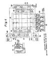
- Fig.4 is a circuit diagram showing a rough configuration of a display device employing a driving method in accordance with one embodiment of the invention.
- Vw emitting threshold voltage
- FIG. 4 only electrodes are shown for the display panel 10 in which data-side electrodes are arranged in the X direction and scanning-side electrodes are arranged in the Y direction.
- Scanning-side n-channel high voltage MOS driver ICs 20 and 30 are pull-down driver circuits for the scanning-side electrodes on the even-numbered and odd-numbered lines respectively, and comprise n-channel MOS transistors NT1-NTi, which are pull-down switching elements, and logic circuits 21 and 31 which comprise shift registers, etc.
- Scanning-side p-channel high voltage MOS driver ICs 40 and 50 are pull-up driver circuits for the scanning-side electrodes on the even-numbered and odd-numbered lines respectively, and comprise p-channel MOS transistors PT1-PTi, which are pull-up switching elements, and logic circuits 41 and 51 which comprise shift registers, etc.
- a data-side driver IC 60 is a push-pull driver circuit for the data-side electrodes, which comprises transistors UT1-UTi having a pull-up function with one terminal thereof connected to a power supply side of transistors DT1-DTi having a pull-down function with one terminal thereof grounded; diodes UD1-UDi, DD1-DDi for flowing currents in the reverse direction from that of the transistors; a logic circuit 70 comprising a shift register, etc. for controlling the switching of the transistors; data inversion control circuits EX1-EXi; and inverting circuits UR1-URi, DR1-DRi.
- the data inversion control circuits EX1-EXi comprise exclusive OR gates, etc. by which display data signals D1-Di output from the logic circuit 70 for controlling the switching of the transistors UT1-UTi, DT1-DTi are inverted in response to a control signal RVC for conversion into signals D1′-Di′. That is, when the control signal RVC is high level, the data inversion control circuits EX1-EXi invert the data signals D1-Di and output them as signals D1′-Di′. On the other hand, when the control signal RVC is low level, the data inversion control circuits EX1-EXi directly output the supplied data signals D1-Di as output signals D1′-Di′ without inverting them.
- Fig.5 is a timing chart explaining the operation for driving a picture element A on a scanning-side electrode Y1 and a picture element B on a scanning-side electrode Y2 in the display panel 10 of the thin-film EL display device.
- the driving of one scanning line during which the positive polarity write voltage Vw+ 1 4 Vm is applied to the scanning-side electrode is referred to as the P driving
- the driving of one scanning line during which the negative polarity write voltage -(Vw- 1 4 Vm) is applied to the scanning-side electrode is referred to as the N driving.
- the reference sign H indicates the waveform of a horizontal synchronizing signal, and the high level period of the waveform is a data valid period.
- the reference sign V indicates the waveform of a vertical synchronizing signal at the rising of which the driving for one frame is initiated.
- the reference sign DLS indicates the waveform of a data latch signal which is output upon completion of the operation of transmitting data for one scanning line in synchronism with a data transmit clock DCK.
- the reference sign RVC indicates the waveform of a data inverting signal, which goes high level during the P driving period to invert all display data signals D1-Di output from the logic circuit 70 during that period.
- the reference sign DATA indicates a display data signal, and the reference signs D1′-Di′ indicate data signals to be input to the transistors UT1-UTi, DT1-DTi in the data-side driver IC. Other signals are described in Table 1.
- the signals RVC, PST, NST, ... are created in a signal generating circuit 111 in synchronism with the horizontal synchronizing signal H and the vertical synchronizing signal V supplied from an image signal source 110 that generates the display data DATA and the data transmit clock DCK.
- a signal generating circuit 111 in synchronism with the horizontal synchronizing signal H and the vertical synchronizing signal V supplied from an image signal source 110 that generates the display data DATA and the data transmit clock DCK.
- corresponding signals are designed by like reference signs but suffixed with "1". These signals are analogous to but different from the signals of this embodiment.
- the polarity of the voltage applied between the scanning-side electrode Y1 and the data-side electrode X2 is set positive, as shown by the reference sign P1 in Fig.5, and then negative, as shown by the reference sign P2, thus reversing the polarity once, for example, to drive the picture element A for light emission.
- the data-side electrode X2 is set at 0V
- the negative polarity voltage P2 is being applied to the scanning-side electrode Y1
- the data-side electrode X2 is set at +30V.
- the desired brightness can be obtained even with a relatively low voltage of 30V applied to the data-side electrode X2.
- the voltage at the data-side electrode X2 as low as 30V as described above, it is possible to reduce the modulation power while achieving the desired brightness with such a low voltage. It is also possible to enhance the brightness by increasing the modulated voltage at the data-side electrode.
- the desired brightness can be obtained without increasing the frequencies of the horizontal synchronizing signal H and vertical synchronizing signal V, there is no need to vary the circuit configuration because of the change in the synchronizing signals H and V.
- the modulated voltage and the write voltage are set with reference to the ground potential, such as the chassis of the display device, as 0 V.
- the display data is high level for emission of light and low level for non-emission of light.
- Fig.6(a) shows the internal configuration of the logic circuit 70.
- the display data DATA for the next scanning line is supplied, in synchronism with the data transmit clock DCK, to a shift register 71 having a storage capacity of one line.
- the data stored in the shift register 71 is transferred to a latch circuit 72 in response to the signal DLS input upon completion of data transmission for one line, and is held in the latch circuit 72 until the end of the driving timing.
- the display data signals D1-Di output from the latch circuit 72 are XORed with the control signal RVC to produce the outputs D1′-Di′ in accordance with which the switching of the transistors UT1-UTi, DT1-DTi′ is controlled.
- the voltage applied to the data-side electrodes X1-Xi is switched at cycles of one horizontal period for every input of the control signal RVC during the horizontal period.
- the control signal RVC input to the data inversion control circuits EX1-EXi is high level during the P driving period and is used to output D1′-Di′ by inverting the display data signals D1-Di input to the data inversion control circuits EX1-EXi during that period.
- the display data signals D1-Di are inverted during the P driving for the following reason.
- the transistors in the p-channel high voltage MOS driver ICs 40 and 50 are turned on so that the potential at the selected scanning-side electrode Y is raised to Vw+ 1 4 Vm while the potential at the selected data-side electrode X, that is, the data-side electrode X containing the picture element to be driven for light emission, is set at 0V.
- a voltage of (Vw+ 1 4 Vm) is applied to the picture element at the intersection of the selected scanning-side electrode Y and selected data-side electrode X to cause the picture element to emit light.
- the potential at the non-selected data-side electrodes X that is, the data-side electrodes X containing picture elements not driven for light emission, is set at is applied to the picture elements at intersections of the non-selected data-side electrodes X and the selected scanning-side electrode Y.
- the applied voltage is below the emitting threshold voltage; therefore, the picture elements are not caused to emit light.
- the transistor UTn connected to the selected data-side electrode Xn is turned off, and the transistor DTn connected thereto is turned on.
- the transistor UTm connected to the non-selected data-side electrode Xm is turned on, and the transistor DTm connected thereto is turned off.
- This requires input data Dn corresponding to the selected data-side electrode Xn to be set low level and input data Dm corresponding to the non-selected data-side electrode Xm to be set high level.
- These levels are the reverse of the levels of the display data DATA input to the data inversion control circuits EX1-EXi. Accordingly, the control signal RVC is required for inverting the display data signals D1-Di.
- the waveform applied to the data-side electrode X2 during the above driving is shown as data-side X2 in Fig.5.
- Fig.6(b) shows the internal configuration of the logic circuits 21, 31 in the n-channel high voltage MOS driver ICs 20, 30, and Fig.6(c) shows the internal configuration of the logic circuits 41, 51 in the p-channel high voltage MOS driver ICs 40, 50.
- the truth table for the logic circuits in the n-channel high voltage MOS driver ICs 20, 30 is shown in Table 2
- the truth table for the logic circuits in the p-channel high voltage MOS driver ICs 40, 50 is shown in Table 3.
- n-channel high voltage MOS driver ICs 20, 30 and the p-channel high voltage MOS driver ICs 40, 50 are complementary to each other. Their logic levels are opposite to each other, but they employ the same configuration. Therefore, the description below deals only with the n-channel high voltage MOS driver ICs 20, 30.
- a shift register 110 is a circuit for storing a selected scanning line and has the function to receive the transmit data NDATA during the high level period of the clock signal CLOCK and output the data NDATA during the low level period of the clock signal CLOCK.
- the signals NSTodd and NSTeven shown in Fig.5 are each used as the clock signal CLOCK and are input to the odd-number n-channel high voltage MOS driver IC 20 and the even-number n-channel high voltage MOS driver IC 30, respectively.
- the transmit data NDATA a signal is input which goes low level only once during one frame period, that is, only during the high level period of the first clock signals NSTodd, NSTeven input after the rising of the vertical synchronizing signal V, as shown in Fig.5.
- the clock signals NSTodd, NSTeven each are input once for every two horizontal periods because the N driving is performed in line sequential fashion with the odd-numbered scanning lines alternating with the even-numbered ones, such as Y1 (odd-numbered line), Y2 (even-numbered line), Y3 (odd-numbered line), and so on.
- a logic circuit 120 is a circuit which uses two input signals NST and NCL for switching the transistors NT1-NTi in the n-channel high voltage MOS driver ICs 20, 30 between three states according to the data from the shift register 110. Its logic is based on the truth table of Table 2. The above operation is summarized in Table 4.
- the operation of the thin-film EL display device is such that both the P driving and the N driving are performed on each line-sequentially selected scanning line, thereby closing an AC pulse required for light emission of each picture element.
- the N driving and the P driving each consist of a modulation period and a write period.
- the modulation period is about 10 ⁇ sec. and the write period is 30 ⁇ sec., thus providing one horizontal period of about 80 ⁇ sec.
- the N-ch source potential and the P-ch source potential shown in Table 4 are the source potentials for transistors of the n-channel high voltage MOS driver ICs 20, 30 and the p-channel high voltage MOS driver ICs 40, 50, respectively, which are required to apply a perfectly symmetrical AC waveform of the amplitude that can cause the picture elements to emit light in the NP and PN fields.
- the signal NSC is a control signal for the source potential switching circuit 90 for the n-channel high voltage MOS driver ICs 20, 30.
- the signal PSC is a control signal for the source potential switching circuit 80 for the p-channel high voltage MOS driver ICs 40, 50.
- NTodd indicates the transistors in the driver IC 20
- NTeven the transistors in the driver IC 30, and "PTodd” the transistors in the driver IC 40.
- ON/OFF means the ON/OFF operation of each of these transistors in each timing.
- (ON) means that only the transistors for the selected scanning line are turned on.
- the ON/OFF/(ON) operations of these transistors are controlled by the signals NCLodd, NSTodd, NCLeven, NSTeven, PCLodd, PSTodd, PCLeven, and PSTeven. Their logic levels in each timing are shown in Table 4.
- the switches SW1 and SW2 are turned off by the signals NSC and PSC respectively, all the transistors in the scanning-side driver ICs 20, 30, 40, and 50 are turned on, and the potential for all the scanning-side electrodes Y is set at 0 V.
- the polarity is reversed between the N driving and the P driving even for the same display data signals D1-Di because of the operation of the data inversion control circuits Ex1-Exi in response to the signal RVC. Therefore, by performing the P driving and the N driving alternately, a perfectly symmetrical alternating current waveform can be obtained for the voltage applied to each picture element.
- the transistor connected to that scanning line is selected from the transistors PTodd in the p-channel high voltage MOS driver IC 40 according to the data from the shift register in the logic circuit 41, and the selected transistor is turned on while the transistors connected to the other scanning lines are turned off. At this time, the transistors PTeven and NTodd are all turned off, and the transistors NTeven are all turned on.
- the driving of the modulation period is continued.
- Figs.7(a) and (b) show the equivalent circuits of the display panel 10 in the above condition.
- the equivalent circuit shown in Fig.7(a) is the one when the picture element A is driven for light emission.
- a negative polarity voltage given by the following equation is applied to the data-side electrode X2 with reference to the scanning-side electrode Y1 so that only the picture element A at the intersection of the data-side electrode X2 and the selected scanning-side electrode Y1 is caused to emit light.
- Fig.7(b) shows the equivalent circuit when the picture element A is not driven to emit light.
- the transistor connected to that scanning line is selected from the transistors NTodd in the n-channel high voltage MOS driver IC 20 according to the data from the shift register in the logic circuit 21, and the selected transistor is turned on while the transistors connected to the other scanning lines are turned off. At this time, the transistors NTeven and PTodd are all turned off, and the transistors PTeven are all turned on.
- the driving of the modulation period is continued.
- Figs.8(a) and (b) show the equivalent circuits of the display panel 10 in the above condition.
- the equivalent circuit shown in Fig.8(a) is the one when the picture element A is driven for light emission.
- a positive polarity voltage given by the following equation is applied to the data-side electrode X2 with reference to the scanning-side electrode Y1 so that only the picture element A at the intersection of the data-side electrode X2 and the selected scanning-side electrode Y1 is caused to emit light.
- Fig.8(b) shows the equivalent circuit when the picture element A is not driven to emit light.
- the signal NSC is set high level to turn on the switch SW2 so that the source potential of the transistors in the n-channel high voltage MOS driver ICs 20, 30 is set at 0 V
- the transistor connected to that scanning line is selected from the transistors PTeven in the p-channel high voltage MOS driver IC 50 according to the data from the shift register in the logic circuit 51, and the selected transistor is turned on while the transistors connected to the other scanning lines are turned off.
- the transistors PTodd and NTeven are all turned off, and the transistors NTodd are all turned on.
- the driving of the modulation period is continued.
- Figs.9(a) and (b) show the equivalent circuits of the display panel 10 in the above condition.
- the equivalent circuit shown in Fig.9(a) is the one when the picture element B is driven for light emission.
- a positive polarity voltage given by the following equation is applied to the data-side electrode X2 with reference to the scanning-side electrode Y2 so that only the picture element B at the intersection of the data-side electrode X2 and the selected scanning-side electrode Y2 is caused to emit light.
- Fig.9(b) shows the equivalent circuit when the picture element B is not driven to emit light.
- the transistor connected to that scanning line is selected from the transistors NTeven in the n-channel high voltage MOS driver IC 30 according to the data from the shift register in the logic circuit 31, and the selected transistor is turned on while the transistors connected to the other scanning lines are turned off. At this time, the transistors NTodd and PTeven are all turned off, and the transistors PTodd are all turned on.
- the driving of the modulation period is continued.
- Figs.10(a) and (b) show the equivalent circuits of the display panel 10 in the above condition.
- the equivalent circuit shown in Fig.10(a) is the one when the picture element B is driven for light emission.
- a positive polarity voltage given by the following equation is applied to the data-side electrode X2 with reference to the scanning-side electrode Y2 so that only the picture element B at the intersection of the data-side electrode X2 and the selected scanning-side electrode Y2 is caused to emit light.
- Fig.10(b) shows the equivalent circuit when the picture element B is not driven to emit light.
- Vm the modulated voltage
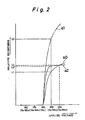
- the brightness L1 of the illuminating picture element of this embodiment will drop significantly as compared with the brightness L0 achieved by the prior art driving method, as shown by the voltage-to-brightness characteristic curve indicated by a0 in Fig.2 of the thin-film EL display device.
- this embodiment is so configured that each picture element is driven at twice the rate of the prior art method without changing the frequencies of the externally supplied synchronizing signals H and V.
- the reference sign a1 indicates the voltage-to-brightness characteristic curve of this embodiment when the number of light emissions per unit time is set, as described above, at twice that of the prior art driving method.
- the resulting light emission brightness L2 is higher than the light emission brightness L0 achieved by the prior art method.
- the modulated voltage is 1 2 Vm, and the number of light emissions per unit time is doubled, i.e.
- the frame frequency is usually 60-Hz
- the time allocated to one frame is about 16.66 msec. Therefore, supposing the time of 40 ⁇ sec. is allocated to each of the N and P driving modes to drive one line of scanning-side electrode Y, it means that about 200 scanning lines can be driven during one frame period.
- the number of scanning lines that can be driven during one frame period will further increase.
- a possible alternative method to double the number of light emissions per unit time may be to perform the P driving twice on every scanning-side electrode during one frame period followed by the N driving to be performed twice on every scanning-side electrode during the next frame period, but this method is not desirable since the characteristic of the EL display device is such that when a voltage of the same polarity is successively applied, the light emission pulse becomes lower in the second emission than in the first emission, thus resulting in a lower brightness than that achieved by the method of this embodiment.
- the P driving is performed, followed by the N driving, on every scanning line during one frame period, but this sequence of driving may be reversed. Also, the driving sequence may be changed for every scanning line.
- the odd-numbered electrodes other than the selected scanning-side electrode are clamped at 0 V, but they may be held in the floating state.
- the polarity of the voltage applied to the EL is reversed only once during the period W12, but the EL may be driven by reversing the polarity of the applied voltage two or more times, which constitutes other embodiments of the invention.
- the write voltage applied to the scanning-side electrode Y as shown in Fig.5 may be modified to provide a waveform shown in Fig.11 so that the polarity of the voltage applied to the picture element A is reversed three times for the driving thereof.
- the modulated voltage for the data-side electrode X2 is varied according to the variation of the voltage applied to the scanning-side electrode Y1, as in the case of the foregoing embodiment.
- Fig.12 shows still another embodiment of the invention, in which the voltage waveform shown in Fig.12(1) is applied to the scanning-side electrode Y1 to drive the picture element A for light emission so that the voltage applied to the picture element A is reversed twice during the period W12.
- the voltage waveform of Fig.12(1) is applied during the scanning of the first frame
- the waveform shown in Fig.12(2) is applied during the subsequent frame period, thereby reliably achieving the desired brightness.
- the selected picture element A is caused to emit light a total of four times during the period W12
- the embodiment of Fig.12 it is caused to emit light a total of three times during that period.
Landscapes
- Engineering & Computer Science (AREA)
- Physics & Mathematics (AREA)
- Computer Hardware Design (AREA)
- General Physics & Mathematics (AREA)
- Theoretical Computer Science (AREA)
- Control Of Indicators Other Than Cathode Ray Tubes (AREA)
- Control Of El Displays (AREA)
Applications Claiming Priority (2)
| Application Number | Priority Date | Filing Date | Title |
|---|---|---|---|
| JP2111375A JP2682886B2 (ja) | 1990-04-25 | 1990-04-25 | 表示装置の駆動方法 |
| JP111375/90 | 1990-04-25 |
Publications (2)
| Publication Number | Publication Date |
|---|---|
| EP0454470A2 true EP0454470A2 (fr) | 1991-10-30 |
| EP0454470A3 EP0454470A3 (en) | 1992-04-01 |
Family
ID=14559595
Family Applications (1)
| Application Number | Title | Priority Date | Filing Date |
|---|---|---|---|
| EP19910303767 Withdrawn EP0454470A3 (en) | 1990-04-25 | 1991-04-25 | A driving method and a driving device for a display device |
Country Status (3)
| Country | Link |
|---|---|
| US (1) | US5206631A (fr) |
| EP (1) | EP0454470A3 (fr) |
| JP (1) | JP2682886B2 (fr) |
Cited By (1)
| Publication number | Priority date | Publication date | Assignee | Title |
|---|---|---|---|---|
| WO2004015669A1 (fr) * | 2002-08-12 | 2004-02-19 | Koninklijke Philips Electronics N.V. | Affichage electroluminescent |
Families Citing this family (11)
| Publication number | Priority date | Publication date | Assignee | Title |
|---|---|---|---|---|
| KR960016720B1 (ko) * | 1993-12-08 | 1996-12-20 | 한국과학기술연구원 | 상대전위차를 이용한 교류구동형 박막 전계발광소자 구동회로 |
| JP2759108B2 (ja) * | 1993-12-29 | 1998-05-28 | カシオ計算機株式会社 | 液晶表示装置 |
| JP3507239B2 (ja) * | 1996-02-26 | 2004-03-15 | パイオニア株式会社 | 発光素子の駆動方法及び装置 |
| GB2313223A (en) * | 1996-05-17 | 1997-11-19 | Sharp Kk | Liquid crystal device |
| JP3049061B1 (ja) * | 1999-02-26 | 2000-06-05 | キヤノン株式会社 | 画像表示装置及び画像表示方法 |
| JP3647013B2 (ja) * | 1998-09-29 | 2005-05-11 | パイオニア株式会社 | 容量性発光素子ディスプレイ装置及びその駆動方法 |
| US20010030511A1 (en) * | 2000-04-18 | 2001-10-18 | Shunpei Yamazaki | Display device |
| US6867755B2 (en) * | 2000-04-28 | 2005-03-15 | Yazaki Corporation | Device and method for driving EL device |
| GB2403841B (en) * | 2003-07-07 | 2006-08-09 | Pelikon Ltd | Control of Electroluminescent displays |
| JP2007086686A (ja) * | 2005-09-26 | 2007-04-05 | Matsushita Toshiba Picture Display Co Ltd | 表示装置 |
| CN103489404B (zh) * | 2013-09-30 | 2016-08-17 | 京东方科技集团股份有限公司 | 像素单元、像素电路及其驱动方法 |
Family Cites Families (16)
| Publication number | Priority date | Publication date | Assignee | Title |
|---|---|---|---|---|
| JPS6088998A (ja) * | 1983-10-21 | 1985-05-18 | 沖電気工業株式会社 | 交流駆動型薄膜el表示パネルの駆動方法 |
| DE3511886A1 (de) * | 1984-04-02 | 1985-10-03 | Sharp K.K., Osaka | Treiberschaltung zum ansteuern eines duennfilm-el-displays |
| JPS60247693A (ja) * | 1984-05-23 | 1985-12-07 | シャープ株式会社 | 薄膜el表示装置の駆動方法 |
| JPH0634151B2 (ja) * | 1985-06-10 | 1994-05-02 | シャープ株式会社 | 薄膜el表示装置の駆動回路 |
| DE3685821T2 (de) * | 1985-10-16 | 1993-02-11 | Sanyo Electric Co | Anzeigeanordnung mit fluessigkristall. |
| JPH0634152B2 (ja) * | 1985-12-17 | 1994-05-02 | シャープ株式会社 | 薄膜el表示装置の駆動回路 |
| JPS62156696A (ja) * | 1985-12-28 | 1987-07-11 | 株式会社東芝 | 薄膜el表示素子の駆動方法 |
| US4691144A (en) * | 1986-01-22 | 1987-09-01 | Planar Systems, Inc. | Staggered refresh pulse generator for a TFEL panel |
| JPH0754377B2 (ja) * | 1986-02-07 | 1995-06-07 | シチズン時計株式会社 | 液晶駆動方式 |
| EP0242468A1 (fr) * | 1986-04-22 | 1987-10-28 | Seiko Instruments Inc. | Dispositif d'affichage à cristaux liquides et méthode de commande pour ce dispositif |
| JPH07109798B2 (ja) * | 1987-01-06 | 1995-11-22 | シャープ株式会社 | 薄膜el表示装置の駆動回路 |
| JPH0748137B2 (ja) * | 1987-07-07 | 1995-05-24 | シャープ株式会社 | 薄膜el表示装置の駆動方法 |
| NL8703040A (nl) * | 1987-12-16 | 1989-07-17 | Philips Nv | Werkwijze voor het besturen van een passieve ferro-elektrisch vloeibaar kristal weergeefinrichting. |
| JPH01227191A (ja) * | 1988-03-07 | 1989-09-11 | Sharp Corp | 表示駆動方法 |
| JPH0681287B2 (ja) * | 1988-07-15 | 1994-10-12 | シャープ株式会社 | 液晶投射装置 |
| GB2225473B (en) * | 1988-11-23 | 1993-01-13 | Stc Plc | Addressing scheme for multiplexded ferroelectric liquid crystal |
-
1990
- 1990-04-25 JP JP2111375A patent/JP2682886B2/ja not_active Expired - Lifetime
-
1991
- 1991-04-22 US US07/688,144 patent/US5206631A/en not_active Expired - Lifetime
- 1991-04-25 EP EP19910303767 patent/EP0454470A3/en not_active Withdrawn
Cited By (1)
| Publication number | Priority date | Publication date | Assignee | Title |
|---|---|---|---|---|
| WO2004015669A1 (fr) * | 2002-08-12 | 2004-02-19 | Koninklijke Philips Electronics N.V. | Affichage electroluminescent |
Also Published As
| Publication number | Publication date |
|---|---|
| US5206631A (en) | 1993-04-27 |
| EP0454470A3 (en) | 1992-04-01 |
| JPH047592A (ja) | 1992-01-10 |
| JP2682886B2 (ja) | 1997-11-26 |
Similar Documents
| Publication | Publication Date | Title |
|---|---|---|
| US4983885A (en) | Thin film EL display panel drive circuit | |
| US5006838A (en) | Thin film EL display panel drive circuit | |
| US4951041A (en) | Driving method for thin film el display device and driving circuit thereof | |
| US4888523A (en) | Driving circuit of thin membrane EL display apparatus | |
| US6911964B2 (en) | Frame buffer pixel circuit for liquid crystal display | |
| US4962374A (en) | Thin film el display panel drive circuit | |
| US20050264514A1 (en) | Shift register | |
| EP0454470A2 (fr) | Méthode et dispositif de commande d'un appareil d'affichage | |
| US4999618A (en) | Driving method of thin film EL display unit and driving circuit thereof | |
| US5627556A (en) | Circuit for driving alternating current thin film electroluminescence device using relative potential difference | |
| JPH0528387B2 (fr) | ||
| JPH0990904A (ja) | El表示装置 | |
| JPH07281641A (ja) | アクティブマトリクス型液晶ディスプレイ | |
| US5032829A (en) | Thin film el display device | |
| US5233340A (en) | Method of driving a display device | |
| JP2728582B2 (ja) | El表示装置の駆動方法 | |
| JP3301379B2 (ja) | El表示装置 | |
| JP2571766B2 (ja) | マトリクス表示パネル | |
| JP2618983B2 (ja) | 薄膜el表示装置の駆動方法 | |
| JPH0232391A (ja) | 表示装置 | |
| JPH0528386B2 (fr) | ||
| JP4360170B2 (ja) | Elディスプレイ表示装置及びelディスプレイの駆動制御方法 | |
| JPH03182793A (ja) | 表示装置の駆動方法 | |
| EP0419184A2 (fr) | Méthode et dispositif de commande d'un appareil d'affichage | |
| JPH0528385B2 (fr) |
Legal Events
| Date | Code | Title | Description |
|---|---|---|---|
| PUAI | Public reference made under article 153(3) epc to a published international application that has entered the european phase |
Free format text: ORIGINAL CODE: 0009012 |
|
| AK | Designated contracting states |
Kind code of ref document: A2 Designated state(s): DE FR GB |
|
| PUAL | Search report despatched |
Free format text: ORIGINAL CODE: 0009013 |
|
| AK | Designated contracting states |
Kind code of ref document: A3 Designated state(s): DE FR GB |
|
| 17P | Request for examination filed |
Effective date: 19920717 |
|
| 17Q | First examination report despatched |
Effective date: 19940307 |
|
| RAP1 | Party data changed (applicant data changed or rights of an application transferred) |
Owner name: SHARP KABUSHIKI KAISHA |
|
| STAA | Information on the status of an ep patent application or granted ep patent |
Free format text: STATUS: THE APPLICATION IS DEEMED TO BE WITHDRAWN |
|
| 18D | Application deemed to be withdrawn |
Effective date: 19940920 |