EP0454981A2 - Statisches Direktzugriffspeicherzellenfeld mit geteiltem Emissor - Google Patents
Statisches Direktzugriffspeicherzellenfeld mit geteiltem Emissor Download PDFInfo
- Publication number
- EP0454981A2 EP0454981A2 EP91104278A EP91104278A EP0454981A2 EP 0454981 A2 EP0454981 A2 EP 0454981A2 EP 91104278 A EP91104278 A EP 91104278A EP 91104278 A EP91104278 A EP 91104278A EP 0454981 A2 EP0454981 A2 EP 0454981A2
- Authority
- EP
- European Patent Office
- Prior art keywords
- bit lines
- memory cell
- cell array
- memory cells
- pair
- Prior art date
- Legal status (The legal status is an assumption and is not a legal conclusion. Google has not performed a legal analysis and makes no representation as to the accuracy of the status listed.)
- Withdrawn
Links
Images


Classifications
-
- G—PHYSICS
- G11—INFORMATION STORAGE
- G11C—STATIC STORES
- G11C11/00—Digital stores characterised by the use of particular electric or magnetic storage elements; Storage elements therefor
- G11C11/21—Digital stores characterised by the use of particular electric or magnetic storage elements; Storage elements therefor using electric elements
- G11C11/34—Digital stores characterised by the use of particular electric or magnetic storage elements; Storage elements therefor using electric elements using semiconductor devices
- G11C11/40—Digital stores characterised by the use of particular electric or magnetic storage elements; Storage elements therefor using electric elements using semiconductor devices using transistors
- G11C11/41—Digital stores characterised by the use of particular electric or magnetic storage elements; Storage elements therefor using electric elements using semiconductor devices using transistors forming static cells with positive feedback, i.e. cells not needing refreshing or charge regeneration, e.g. bistable multivibrator or Schmitt trigger
- G11C11/411—Digital stores characterised by the use of particular electric or magnetic storage elements; Storage elements therefor using electric elements using semiconductor devices using transistors forming static cells with positive feedback, i.e. cells not needing refreshing or charge regeneration, e.g. bistable multivibrator or Schmitt trigger using bipolar transistors only
- G11C11/4116—Digital stores characterised by the use of particular electric or magnetic storage elements; Storage elements therefor using electric elements using semiconductor devices using transistors forming static cells with positive feedback, i.e. cells not needing refreshing or charge regeneration, e.g. bistable multivibrator or Schmitt trigger using bipolar transistors only with at least one cell access via separately connected emittors of said transistors or via multiple emittors, e.g. T2L, ECL
-
- G—PHYSICS
- G11—INFORMATION STORAGE
- G11C—STATIC STORES
- G11C11/00—Digital stores characterised by the use of particular electric or magnetic storage elements; Storage elements therefor
- G11C11/21—Digital stores characterised by the use of particular electric or magnetic storage elements; Storage elements therefor using electric elements
- G11C11/34—Digital stores characterised by the use of particular electric or magnetic storage elements; Storage elements therefor using electric elements using semiconductor devices
- G11C11/40—Digital stores characterised by the use of particular electric or magnetic storage elements; Storage elements therefor using electric elements using semiconductor devices using transistors
- G11C11/41—Digital stores characterised by the use of particular electric or magnetic storage elements; Storage elements therefor using electric elements using semiconductor devices using transistors forming static cells with positive feedback, i.e. cells not needing refreshing or charge regeneration, e.g. bistable multivibrator or Schmitt trigger
- G11C11/413—Auxiliary circuits, e.g. for addressing, decoding, driving, writing, sensing, timing or power reduction
- G11C11/414—Auxiliary circuits, e.g. for addressing, decoding, driving, writing, sensing, timing or power reduction for memory cells of the bipolar type
- G11C11/416—Read-write [R-W] circuits
Definitions
- This invention relates generally to the static, random access, semiconductor memory arrays and, more specifically, to a static random access memory array which incorporates split-emitter memory cells.
- the latter are accessed during a read cycle of a selected memory cell by precharging all the bit lines of unselected memory cells associated with the word line of the selected cell. This is accomplished by switchably connecting a voltage source to all the unselected bit lines which charges their bit line capacitances. Then, when read current sources are switchably connected to both the selected and unselected memory cells and the associated word is switched to a WORD SELECT source, the read current associated with the unselected bit lines flows via charging switches to the precharge voltage sources and the read current associated with the selected bit lines flows into the selected cell.
- FIG. 1 of the present application shows a memory cell identical to Fig. 1 of the article which will be discussed hereinbelow in some detail. Also, while the article goes into detail to show the read-write selection approaches used, Fig.
- an object of the present invention to reduce additional delay during a read cycle due to a worst-case bit pattern on the memory cell array while simultaneously minimizing required drive power.
- Another object of the present invention is to provide for the precharging of unselected bit lines so that upon actuation of the read current sources to all bit lines, the read currents of the selected cell flow to the selected word line.
- Yet another object of the present invention is to prevent dynamic currents of unselected cells from flowing into the booster resisters of the selected cell by charging only the bit line capacitances of unselected cells.
- Still another object of the present invention is to provide a cell selection approach which minimizes cell read delay.
- This invention relates to static, random access, semiconductor memory arrays which utilize split-emitter memory cells.
- a selected memory cell is accessed during a read cycle by subjecting all the bit lines of unselected memory cells associated with the same word line of the selected cell to a precharge of their bit line capacitances.
- Voltage sources are connected via actuatable switches to each of the unselected bit lines to charge their bit line capacitances.
- the read current associated with the unselected bit lines flows via the charging switches to the precharge voltage sources.
- the read current associated with the selected bit lines flows into the selected cell where the differential voltage across the cell is sensed by an associated sense amplifier.
- bit line capacitances of the unselected cells are precharged, large dynamic word line currents are not present.
- present cell select approach virtually eliminates any dynamic incorrect read signal such as occurs when a worst-case bit pattern appears in conventional read select approaches. Also, read delays are minimized so that the overall access time is also minimized because all portions of the read cycle begin substantially simultaneously.
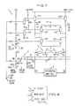
- Fig. 1 shows a schematic diagram of a prior art split-emitter cell which is utilized in an array of memory cells in the practice of the present invention.
- NPN transistors T1,T2 are inverting transistors while PNP transistors T3,T4 serve as load devices.
- Bit lines B0,B1 are shown connected to the emitter of transistors T3,T4, respectively, while emitters of transistors T1,T2 are coupled via booster resistor R1,R2 to the word address line, W-ADDRESS.
- the collectors of transistors T1,T2 are cross-coupled to the bases of transistors T2,T1, respectively.
- the memory cell of Fig. 1 is described and discussed in detail in the IEEE Journal of Solid-State Circuits, Vol.
- a cell delay of about 5 nanoseconds has been achieved based on a prior art cell select scheme shown in the following Fig. 2.
- a major drawback of the prior art approach shown in Fig. 2 is the fact that the cell read delay is considerably increased if a "worst-case" bit pattern ("0" in all memory cells except the selected cell) is experienced by the memory array.
- Fig. 2 is a partially schematic, partially block diagram of a prior art memory array using the split-emitter memory cells of Fig. 1 which, though it shows but four cells, is representative of memory arrays incorporating thousands of such cells.
- memory array 1 includes a plurality of split-emitter memory cells 2 arranged in rows and columns.
- Differential amplifiers 3 are shown connected to pairs of bit lines B0,B1 which are, in turn, connected to memory cells 2 via interconnections 4,5. Interconnections 4,5 connect bit lines B0,B1 to the emitters of transistors T3,T4, respectively, shown in Fig. 1.
- Bit lines B0,B1 each have bit line capacitances represented in Fig.
- bit line pairs B0,B1 are connected to a source of reference voltage VREF1 which, for present purposes, has a value of zero (0) volts.
- a bit line switch, S1 is shown serially disposed in each of the bit line pairs B0,B1. Switches S1 are closed in the standby mode connecting bit lines B0,B1 and their associated capacitances CB0, CB1 to VREF1.
- Read-write current sources 6 are shown in Fig. 2 connected to each bit line, B0,B1 via a read current switch S2 which is open in standby mode. Read current, Io, is provided to each of the bit lines B0,B1 when switch S2 is closed.
- Memory cells 2 in Fig. 2 are shown connected to a word select source 7 via common booster resistors RBW, word line interconnections 8 and word select switch S3.
- Interconnections 8 connect to the emitters of transistors T1,T2 of the memory cell shown in Fig. 1.
- Sources 7 include two sources, voltage source, VREFW and standby current source, ISTB. The latter is normally connected via one contact of switch S3 to an interconnection 8. When word select switch S3 is actuated, however, an interconnection 8 is connected via the other contact of S3 to voltage source, VREFW.
- the left hand pair of bit lines, B0,B1 are associated with a column of memory cells 2 otherwise identified in Fig. 2 as DIGIT 1.
- the right hand pair of bit lines B0,B1 are associated with a column of memory cells 2 identified as DIGIT 2.
- the uppermost row of memory cells 2 is otherwise identified as WORD 1 and the lowermost row of cells 2 is otherwise identified as WORD 2.
- memory cell 2 associated with DIGIT 1, WORD 1 can be otherwise identified in Fig. 2 as cell 1,1.
- Cell 1,2, cell 2,1 and cell 2,2 are similarly identified using the same associations.
- Fig. 3 is a graphical representation showing the position of switches S1, S2, S3 versus time when a prior art cell selection approach for a read operation is used in conjunction with the memory array of Fig. 2.
- switch S1 is first actuated at time, t1, as shown in Fig. 3.
- Actuation of switch S1 disconnects bit lines B0,B1 associated with cell 1,1 from their standby power supply, VREF1.
- read current sources 6 of the selected bit line pair B0,B1 associated with cell 1,1 are connected to those bit lines by actuating switches S2.
- switch S3 is disconnected from source ISTB and connected to source VREFW, pulling the selected word line down to a lower voltage.
- source ISTB is -0.6 volts and VREFW is -1.1 volts
- the selected word line is pulled down by about 500mV. Due to this lowering of voltage in the selected word line, the read current, Io, flows into memory cell 1,1 only, causing a voltage difference at the associated bit lines, B0,B1 depending on the state of memory cell 1,1. Note that no read current, Io, flows into memory cell 1,2 because, even though associated with a selected word line, it is also associated with unselected bit lines whose switches S2 are unactuated.
- Fig. 4 there is shown a plot of Bit Line Sense Signals and Word Line Voltage in volts versus Time in nanoseconds when prior art or conventional sensing approaches are utilized.
- the plot shows the sense signals obtained when a symmetrical bit pattern (when fifty percent of the cells of the array store a binary one and the remaining fifty percent of the cells store a binary zero) has been stored in the array of Fig. 2 and when a worst-case bit pattern is stored in the same array.
- the former pattern produces a read delay of approximately 5 ns while the latter pattern produces a read delay of approximately 11 ns.
- the large delay produced when a worst-case bit pattern is stored in the array is unacceptable because the overall circuit design must take into account the possibility that such large delays will occur.
- the circuit shown in Fig. 5 not only reduces the delay due to worst-case bit patterns, but also reduces it to a value less than that obtained for symmetrical bit patterns using the prior art circuit of Fig. 3.
- Fig. 5 is a partially schematic, partially block diagrammatic circuit of a split-emitter memory cell array which, among other things, incorporates a means for precharging unselected bit lines slightly before the application of a word select signal.
- the same reference characters which were used in Fig. 3 are used in Fig. 5 where the elements which they identify are the same.
- the circuits of Fig. 3 and Fig. 5 are identical except that switches S1 and S2 of Fig. 3 have been combined into a switch S12 in Fig. 5 and a new precharging switch S13, which connects a precharging source, VREF2, to each of the bit lines, B0,B1, has been added.
- switch S12 provides standby, restore or read currents depending on whether it is connected to source 6 or VREF1.
- Switch S13 provides for unselected bit line precharge and S3 provides for word line selection or standby depending on whether it is connected to VREFW or ISTB.
- Fig. 6 shows the condition of switches S12, S13, and S3 versus time which, when actuated as shown in the circuit of Fig. 5, minimizes all the possible read delays.
- switches S12 are first actuated disconnecting both selected and unselected bit lines from source VREF1. At substantially the same time, switches S12 connect read current sources 6 to both the selected and unselected bit lines B0,B1. Slightly after switches S12 are actuated, switches S13 associated with all the unselected bit lines B0,B1, are actuated precharging the capacitances CB0,CB1 associated with the unselected bit line B0,B1 to about -0.6V.
- switch S3 associated with memory cell 1,1 is actuated changing the voltage on interconnections 8 from ISTB to VREFW dropping the voltage on interconnections 8 by about 500mV.
- the read currents Io from sources 6 flow in both the selected and unselected bit lines. In the latter, currents Io flow into sources VREF2 which are still connected to bit line B0,B1 via switches S13 which are still in their actuated state. This occurs because switches S13 present an essentially short-circuit path to sources VREF2 as opposed to a higher resistance path through cell 1,2, for example.
- FIG. 7 there is shown a schematic diagram of a portion of the arrangement shown in Fig. 5 both of which are implementations of a cell select scheme with parallel bit line precharge.
- Fig. 7 shows but a single memory cell, its associated bit and word lines and associated circuitry which apply the pulsed waveforms shown in Fig. 8 to it to carry out the functions of word and bit decoding, precharging, reading and the like. Where applicable, the same reference characters have been utilized in Fig. 7 as were used in FIGS. 2 and 5.
- memory cell 2 consisting of devices T1-T4 are connected as shown in Fig. 1 to bit lines B0,B1 via interconnections 4,5, respectively, and to word line interconnections 8.
- a pair of NPN transistors, S12, serially disposed in bit lines B0,B1 are connected at their collectors to VREF1 and supply restore and standby potentials to the bit lines.
- a pair of read current pnp transistors, S12' connected at their emitters to a read current source 6 (otherwise identified in Fig. 7 as ITOTAL) and at their collectors to bit lines B0,B1, provide read currents Io when rendered conductive by a signal applied to a terminal 9 otherwise identified in Fig. 7 as SELECT CLOCK.
- a pair of npn precharge transistors S13 are connected at their emitters to a precharge voltage source VREF2 and at their collectors to bit lines B0,B1.
- Transistors S13 are controlled by signals on their bases from node N1.
- the potential on node N1 is, in turn, controlled by a signal on terminal 10 otherwise identified in Fig. 7 as BIT DECODE.
- a signal on terminal 10 otherwise identified in Fig. 7 as BIT DECODE When the bit decode signal on terminal 10 falls, diode D1 is conductive and the potential on node N1 is such that transistors S13 are rendered nonconductive.
- the bit decode signal is high, diode D1 is rendered nonconductive and a current from V cc renders transistors S13 conductive.
- word line interconnections 8 with their serially disposed resistors R1,R2 are normally connected to a standby voltage source ISTB via a diode D10 which acts as the normally closed portion of word select switch S3.
- An npn transistor T30 is connected at its collector in parallel with diode D10 and its emitter is connected to VREFW.
- the base of transistor T30 is connected to a node N2 which is disposed between a resistor and a diode D20 which form an inverter.
- Diode 20 is connected to a terminal 11 otherwise identified in Fig. 7 as WORD SELECT.
- diode D20 When the word select signal is low, diode D20 is conductive and the potential appearing at node N2 and at the base of transistor T30 renders it nonconductive. When the word select signal rises, diode D20 is rendered nonconductive and a current from V cc flows to the base of transistor T30 rendering it conductive and lowering the word line potential to VREFW, when the signal at SELECT CLOCK is high.
- bit lines B0,B1 in Fig. 7 Assuming bit lines B0,B1 in Fig. 7 to be selected bit lines, the circuit of Fig. 7 operates as follows. When the signal at SELECT CLOCK rises, it causes npn transistor T10 to become conductive applying zero potential to the bases of transistors S12 turning these devices OFF and isolating voltage source VREF1 from bit lines B0,B1. At the same time, all unselected bit lines are disconnected from voltage source VREF1.
- npn device T20 is also rendered conductive, placing zero volts on the bases of pnp transistors S12' turning these devices ON, supplying read currents Io from ITOTAL which pass to memory cell 2. In passing through memory cell 2, they imbalance one side or the other depending on the state of the cell. This action duplicates the action of switch 12 in Fig. 6 which when actuated isolates bit line B0,B1 from VREF1 and causes Io to flow into the bit lines and from thence to memory cell 2.
- bit lines B0,B1 are selected, they remain disconnected from VREF2.
- the BIT SELECT signal at terminal 10 goes low causing diode D1 to conduct placing the low signal on node N1. This causes npn devices S13 to become inoperative, preventing bit line capacitances CB0,CB1 from precharging to VREF2.
- bit line capacitances CB0,CB1 must be precharged, and therefore transistors S13 are rendered conductive.
- node N1 receives a current from V cc which, when applied to the bases of devices S13, renders them conductive thereby precharging the bit line capacitances CB0,CB1 to the potential of VREF2.
- bit lines B0,B1 are being selected, a word line is being similarly selected.
- diode D10 in series with ISTB is conductive and maintains memory cell 2 in the condition in which it was previously written.
- npn device T30 which forms a part of S3, is maintained in the OFF condition because diode D20 is conducting with the WORD SELECT signal on terminal 11 in the low or unselected condition.
- diode D20 ceases conducting and V cc delivers a current to node N2.
- bit lines B0,B1 are disconnected from the VREF1 supply; the current sources supplying read current, Io, are activated; the precharge function in conjunction with a BIT SELECT signal is enabled and the word select function in conjunction with a WORD SELECT signal is also enabled. Since the WORD SELECT output signal generally has the longest path delay, all the other functions are deliberately delayed by the SELECT CLOCK resulting in a minimum cell access time. As shown by the curves of the bit line sense signals in Fig. 9, not only has the delay variation between symmetrical and worst-case bit patterns been reduced, but the delay for the worst-case bit pattern for the circuit of Fig.
- the circuit of Fig. 7 provides a substantially reduced cell access time since the large worst-case bit pattern delay of the prior art has been substantially reduced.
- the access time variation between symmetrical and worst-case bit pattern delays of the prior art has been reduced and all functions are carried out using a single clock.
- there are no resistors in the select, precharge and restore paths only very small voltage swings are required for bit line, word line and control signals resulting in a good speed/power ratio for peripheral circuits.
Landscapes
- Engineering & Computer Science (AREA)
- Microelectronics & Electronic Packaging (AREA)
- Computer Hardware Design (AREA)
- Static Random-Access Memory (AREA)
- Semiconductor Memories (AREA)
Applications Claiming Priority (2)
| Application Number | Priority Date | Filing Date | Title |
|---|---|---|---|
| US516648 | 1990-04-30 | ||
| US07/516,648 US5121357A (en) | 1990-04-30 | 1990-04-30 | Static random access split-emitter memory cell selection arrangement using bit line precharge |
Publications (2)
| Publication Number | Publication Date |
|---|---|
| EP0454981A2 true EP0454981A2 (de) | 1991-11-06 |
| EP0454981A3 EP0454981A3 (en) | 1993-01-27 |
Family
ID=24056524
Family Applications (1)
| Application Number | Title | Priority Date | Filing Date |
|---|---|---|---|
| EP19910104278 Withdrawn EP0454981A3 (en) | 1990-04-30 | 1991-03-20 | A static random access split-emitter memory cell array |
Country Status (3)
| Country | Link |
|---|---|
| US (1) | US5121357A (de) |
| EP (1) | EP0454981A3 (de) |
| JP (1) | JPH07122994B2 (de) |
Families Citing this family (2)
| Publication number | Priority date | Publication date | Assignee | Title |
|---|---|---|---|---|
| US5297089A (en) * | 1992-02-27 | 1994-03-22 | International Business Machines Corporation | Balanced bit line pull up circuitry for random access memories |
| KR100555534B1 (ko) * | 2003-12-03 | 2006-03-03 | 삼성전자주식회사 | 인액티브 위크 프리차아징 및 이퀄라이징 스킴을 채용한프리차아지 회로, 이를 포함하는 메모리 장치 및 그프리차아지 방법 |
Family Cites Families (11)
| Publication number | Priority date | Publication date | Assignee | Title |
|---|---|---|---|---|
| US3573758A (en) * | 1969-02-27 | 1971-04-06 | Ibm | Non-linear impedance means for transistors connected to each other and to a common power source |
| DE2926094A1 (de) * | 1979-06-28 | 1981-01-08 | Ibm Deutschland | Verfahren und schaltungsanordnung zum entladen von bitleitungskapazitaeten eines integrierten halbleiterspeichers |
| EP0078335B1 (de) * | 1981-10-30 | 1986-02-05 | Ibm Deutschland Gmbh | Verfahren zum Lesen eines Halbleiterspeichers |
| JPS59112723A (ja) * | 1982-12-20 | 1984-06-29 | Hitachi Ltd | 半導体回路 |
| JPS59151386A (ja) * | 1983-01-31 | 1984-08-29 | Fujitsu Ltd | 半導体記憶装置 |
| JPS61290755A (ja) * | 1985-06-19 | 1986-12-20 | Hitachi Ltd | 半導体記憶装置 |
| JPH0746510B2 (ja) * | 1985-10-25 | 1995-05-17 | 日立超エル・エス・アイエンジニアリング株式会社 | 半導体記憶装置 |
| JPS61180994A (ja) * | 1986-01-24 | 1986-08-13 | Hitachi Ltd | 半導体回路 |
| US4769785A (en) * | 1986-06-02 | 1988-09-06 | Advanced Micro Devices, Inc. | Writing speed of SCR-based memory cells |
| US4858183A (en) * | 1987-06-02 | 1989-08-15 | Texas Instruments Incorporated | ECL high speed semiconductor memory and method of accessing stored information therein |
| US4864540A (en) * | 1988-02-11 | 1989-09-05 | Digital Equipment Corporation | Bipolar ram having no write recovery time |
-
1990
- 1990-04-30 US US07/516,648 patent/US5121357A/en not_active Expired - Fee Related
-
1991
- 1991-03-20 EP EP19910104278 patent/EP0454981A3/en not_active Withdrawn
- 1991-03-29 JP JP3135400A patent/JPH07122994B2/ja not_active Expired - Lifetime
Also Published As
| Publication number | Publication date |
|---|---|
| JPH04228184A (ja) | 1992-08-18 |
| EP0454981A3 (en) | 1993-01-27 |
| JPH07122994B2 (ja) | 1995-12-25 |
| US5121357A (en) | 1992-06-09 |
Similar Documents
| Publication | Publication Date | Title |
|---|---|---|
| US5093806A (en) | Sensing and decoding scheme for a bicmos read/write memory | |
| US4866674A (en) | Bitline pull-up circuit for a BiCMOS read/write memory | |
| US3949385A (en) | D.C. Stable semiconductor memory cell | |
| US3993917A (en) | Parameter independent FET sense amplifier | |
| US4156941A (en) | High speed semiconductor memory | |
| US4862421A (en) | Sensing and decoding scheme for a BiCMOS read/write memory | |
| US4078261A (en) | Sense/write circuits for bipolar random access memory | |
| JPS5812676B2 (ja) | センス増幅器 | |
| US5058067A (en) | Individual bit line recovery circuits | |
| GB1536013A (en) | Data storage memories | |
| US4926383A (en) | BiCMOS write-recovery circuit | |
| US4598387A (en) | Capacitive memory signal doubler cell | |
| US4280198A (en) | Method and circuit arrangement for controlling an integrated semiconductor memory | |
| US4168539A (en) | Memory system with row clamping arrangement | |
| US4404662A (en) | Method and circuit for accessing an integrated semiconductor memory | |
| JPH01173393A (ja) | 参照電圧回復回路及びこれを用いたメモリ装置 | |
| US4864540A (en) | Bipolar ram having no write recovery time | |
| US3629612A (en) | Operation of field-effect transistor circuit having substantial distributed capacitance | |
| US5051955A (en) | Semiconductor memory having improved data readout scheme | |
| US3364362A (en) | Memory selection system | |
| JPH022239B2 (de) | ||
| US5121357A (en) | Static random access split-emitter memory cell selection arrangement using bit line precharge | |
| US4319344A (en) | Method and circuit arrangement for discharging bit line capacitances of an integrated semiconductor memory | |
| JPH04229491A (ja) | 自己ブースト耐性を有するbicmos論理回路および方法 | |
| EP0031462B1 (de) | Differenzial Ladungslesesystem für eine aus 4 Teile bestehende MTL Speicherzelle |
Legal Events
| Date | Code | Title | Description |
|---|---|---|---|
| PUAI | Public reference made under article 153(3) epc to a published international application that has entered the european phase |
Free format text: ORIGINAL CODE: 0009012 |
|
| AK | Designated contracting states |
Kind code of ref document: A2 Designated state(s): DE FR GB |
|
| 17P | Request for examination filed |
Effective date: 19911219 |
|
| PUAL | Search report despatched |
Free format text: ORIGINAL CODE: 0009013 |
|
| AK | Designated contracting states |
Kind code of ref document: A3 Designated state(s): DE FR GB |
|
| 17Q | First examination report despatched |
Effective date: 19950224 |
|
| STAA | Information on the status of an ep patent application or granted ep patent |
Free format text: STATUS: THE APPLICATION IS DEEMED TO BE WITHDRAWN |
|
| 18D | Application deemed to be withdrawn |
Effective date: 19950707 |