EP0458246B1 - Halbleiterherstellungseinrichtung - Google Patents
Halbleiterherstellungseinrichtung Download PDFInfo
- Publication number
- EP0458246B1 EP0458246B1 EP91108150A EP91108150A EP0458246B1 EP 0458246 B1 EP0458246 B1 EP 0458246B1 EP 91108150 A EP91108150 A EP 91108150A EP 91108150 A EP91108150 A EP 91108150A EP 0458246 B1 EP0458246 B1 EP 0458246B1
- Authority
- EP
- European Patent Office
- Prior art keywords
- chip carrier
- depressing
- concave portion
- rotor
- disposed
- Prior art date
- Legal status (The legal status is an assumption and is not a legal conclusion. Google has not performed a legal analysis and makes no representation as to the accuracy of the status listed.)
- Expired - Lifetime
Links
Images

Classifications
-
- H—ELECTRICITY
- H10—SEMICONDUCTOR DEVICES; ELECTRIC SOLID-STATE DEVICES NOT OTHERWISE PROVIDED FOR
- H10P—GENERIC PROCESSES OR APPARATUS FOR THE MANUFACTURE OR TREATMENT OF DEVICES COVERED BY CLASS H10
- H10P72/00—Handling or holding of wafers, substrates or devices during manufacture or treatment thereof
- H10P72/70—Handling or holding of wafers, substrates or devices during manufacture or treatment thereof for supporting or gripping
- H10P72/76—Handling or holding of wafers, substrates or devices during manufacture or treatment thereof for supporting or gripping using mechanical means, e.g. clamps or pinches
- H10P72/7604—Handling or holding of wafers, substrates or devices during manufacture or treatment thereof for supporting or gripping using mechanical means, e.g. clamps or pinches the wafers being placed on a susceptor, stage or support
- H10P72/7606—Handling or holding of wafers, substrates or devices during manufacture or treatment thereof for supporting or gripping using mechanical means, e.g. clamps or pinches the wafers being placed on a susceptor, stage or support characterised by edge clamping, e.g. clamping ring
-
- H—ELECTRICITY
- H10—SEMICONDUCTOR DEVICES; ELECTRIC SOLID-STATE DEVICES NOT OTHERWISE PROVIDED FOR
- H10P—GENERIC PROCESSES OR APPARATUS FOR THE MANUFACTURE OR TREATMENT OF DEVICES COVERED BY CLASS H10
- H10P72/00—Handling or holding of wafers, substrates or devices during manufacture or treatment thereof
- H10P72/70—Handling or holding of wafers, substrates or devices during manufacture or treatment thereof for supporting or gripping
- H10P72/76—Handling or holding of wafers, substrates or devices during manufacture or treatment thereof for supporting or gripping using mechanical means, e.g. clamps or pinches
- H10P72/7604—Handling or holding of wafers, substrates or devices during manufacture or treatment thereof for supporting or gripping using mechanical means, e.g. clamps or pinches the wafers being placed on a susceptor, stage or support
- H10P72/7622—Handling or holding of wafers, substrates or devices during manufacture or treatment thereof for supporting or gripping using mechanical means, e.g. clamps or pinches the wafers being placed on a susceptor, stage or support characterised by supporting substrates others than wafers, e.g. chips
-
- H—ELECTRICITY
- H10—SEMICONDUCTOR DEVICES; ELECTRIC SOLID-STATE DEVICES NOT OTHERWISE PROVIDED FOR
- H10W—GENERIC PACKAGES, INTERCONNECTIONS, CONNECTORS OR OTHER CONSTRUCTIONAL DETAILS OF DEVICES COVERED BY CLASS H10
- H10W72/00—Interconnections or connectors in packages
- H10W72/50—Bond wires
-
- H—ELECTRICITY
- H10—SEMICONDUCTOR DEVICES; ELECTRIC SOLID-STATE DEVICES NOT OTHERWISE PROVIDED FOR
- H10W—GENERIC PACKAGES, INTERCONNECTIONS, CONNECTORS OR OTHER CONSTRUCTIONAL DETAILS OF DEVICES COVERED BY CLASS H10
- H10W72/00—Interconnections or connectors in packages
- H10W72/50—Bond wires
- H10W72/551—Materials of bond wires
- H10W72/552—Materials of bond wires comprising metals or metalloids, e.g. silver
Definitions
- This invention relates to a semiconductor manufacturing apparatus for mounting an optical semiconductor element on a chip carrier, for example, and more particularly to a semiconductor manufacturing apparatus capable of mounting various types of chip carriers precisely in a preset position on a stage at any time.
- optical semiconductor elements are sometimes incorporated into an optical communication module.
- the optical semiconductor elements are separately mounted on chip carriers formed of ceramics, for example, to simplify the incorporation into and the maintenance of the optical communication module.
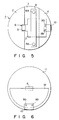
- Figs. 5 and 6 show conventional semiconductor manufacturing apparatuses.
- the optical semiconductor element is mounted on the chip carrier by use of the above manufacturing apparatus.
- a circular stage 1 is formed of metal and can be heated.
- the surface of the stage 1 has first, second and third surfaces 2, 3 and 4 and stepped portions are formed between the first and second surfaces 2 and 3 and between the second and third surfaces 3 and 4.
- a rectangular concave portion 6 for positioning a chip carrier 5 is formed in the central portion of the stepped portion between the first and second surfaces 2 and 3.
- the carrier chip 5 is mounted in the concave portion 6 on the second surface 3.
- the chip carrier 5 is depressed against the side surface of the concave portion 6 by a depressing plate 7 which is movably disposed on the second surface 3 and fixed in the position.
- a holding plate 8 disposed on the depressing plate 7 has both ends in the lengthwise direction thereof fixed on the second surface 3 by means of screws 9a and a gap in which the depressing plate 7 can be moved is provided between the holding plate 8 and the second surface 3.
- the depressing plate 7 is fixed on a clamp portion 10 by means of screws 9b and the clamp portion 10 is disposed to freely move on the third surface 4.
- the chip carrier 5 is mounted on the circular plate-like metal stage 11 which can be heated, a semi-circular depressing plate 12 is mounted on one end portion of the chip carrier 5, and the chip carrier 5 is depressed against the stage 11 by means of the depressing plate 12 and fixed there.
- a chip carrier is extremely small and is generally several mm square. Therefore, as shown in Fig. 6, when one end portion of the chip carrier 5 is depressed by the depressing plate 12, the other end portion of the chip carrier is lifted from the stage 11 and the chip carrier cannot be fixedly positioned. Further, when the chip carrier 5 is depressed by means of the depressing plate 12, a metal film such as an electrode which covers the surface of the chip carrier 5 may be sometimes damaged.
- An object of this invention is to provide a semiconductor manufacturing apparatus which can hold a chip carrier precisely in a preset position so that an optical semiconductor element can be accurately mounted on the chip carrier and at the same time which can precisely hold various types of chip carriers without damaging the chip carrier.
- a semiconductor manufacturing apparatus comprising: a stage having
- the concave portion of circular arc form is formed in the side surface connecting the first and second surfaces to each other or the depressing surface of the depressing plate.
- the chip carrier mounted on the second surface is held between the circular arc-form concave portion formed in the side surface and the depressing surface of the depressing plate or between the side surface and the circular arc-form concave portion formed in the depressing surface of the depressing plate.
- the chip carrier receives force acting towards the center of the circular arc-form concave portion to move along the circular arc-form concave portion and is always fixed in a preset position on the second surface irrespective of the position in which the chip carrier is placed before being fixed.
- an optical semiconductor element can be precisely mounted on the chip carrier.
- the chip carrier can be stably fixed irrespective of the shape thereof.
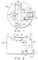
- Figs. 1 and 2 show one embodiment of a semiconductor manufacturing apparatus of this invention.
- a circular stage 20 is formed of metal and can be heated.
- the surface of the stage 20 has first, second and third surfaces 21, 22 and 23 formed in a stepped configuration.
- a first side surface 21a is formed between the first and second surfaces 21 and 22 and a second side surface 22a is formed between the second and third surfaces 22 and 23.
- the second surface 22 is lower than the first surface 21 and the third surface 23 is lower than the second surface 22.
- a circular arc-form concave portion 24 for positioning a chip carrier 41 is formed in the central portion of the first side surface 21a.
- the circular arc-form concave portion 24 has a side surface 24a formed in a circular arc form and the second surface 22 is exposed through the concave portion 24.
- the chip carrier 41 is disposed on the second surface 22 inside the concave portion 24.
- a plurality of electrodes (not shown) which are electrically insulated are formed by plating on the surface of the chip carrier 41.
- a depressing plate 26 for fixing the chip carrier is disposed on the second surface 22.
- the depressing plate 26 is disposed so as to freely slide in a direction perpendicular to the first side surface 21a on the second surface 22. That is, a holding plate 28 is fixed on the second surface 22 by means of screws 40a.
- a gap in which the depressing plate 26 can slide is formed between the holding plate 28 and the second surface 22, and the depressing plate 26 is set inside the gap.
- a depressing portion 25 for depressing the chip carrier against the circular arc form side surface 24a is disposed on that portion of the depressing plate 26 which faces the circular arc form side surface 24a of the concave portion 24.
- the surface of the depressing portion 25 which is set in contact with the chip carrier is set in parallel with the first side surface 21a.
- the depressing plate 26 is connected to one end of a clamp member 27 by means of screws 40b.
- the clamp member 27 is disposed to freely slide on the third surface.
- the other end of the clamp member 27 is connected to one end of a rotor 30 via a shaft 29.
- the rotor 30 is disposed in a groove 31 formed in the stage 20.
- the groove 31 has an inclined portion 31a formed at the lower portion thereof and the intermediate portion of the rotor 30 is supported on the stage 20 by a shaft 32.
- the rotor 30 may freely rotate around the shaft 32 in the groove 31.
- the clamp member 27 has an inclined portion 27a formed at the intermediate portion thereof and is disposed to move on the third surface 23 with rotation of the rotor 30.
- a spring 33 is disposed between the other end of the rotor 30 and the internal surface of the groove 31 and the rotor 30 is always biased in a direction indicated by an arrow A in the drawing. Further, a button 34 which is depressed to push the rotor 30 against the biasing force of the spring 33 is disposed on the other end of the rotor 30.
- the depressing plate 26 is moved towards the deepest portion of the concave portion 24 and the side surface of the chip carrier 41 is depressed against the depressing surface 25 of the depressing plate 26.
- the opposite side surface (corner portion) of the chip carrier slides on the circular arc-form side surface 24a of the concave portion 24 and is stopped when the side surface of the chip carrier 41 becomes parallel to the depressing surface 25.
- the chip carrier 41 is fixed in position by means of the circular arc-form side surface 24a and the depressing surface 25 of the depressing plate 26.
- the light receiving element 41a is bonded by soldering to a preset portion of the electrode (not shown) on the chip carrier 41. After this, the electrode terminal of the light receiving element 41a is connected to another electrode (not shown) on the chip carrier 41 via a metal wire (not shown).
- the chip carrier 41 of the same shape can be fixed in the preset position on the second surface 22.
- the fixed position of the chip carrier 41 is set to a position in which the side surface of the chip carrier 41 is set in parallel with the depressing portion 25 of the depressing plate 26 and set in contact with the circular arc-form side surface 24a.
- the chip carrier is fixed in the preset position on the stage 20 by means of the circular arc-form concave portion 24 and the depressing portion 25 of the depressing plate 26. Therefore, the chip carrier 41 of the same shape can be always fixed in the same position on the second surface 22. Further, if the chip carrier is smaller than the maximum arc length of the concave portion 24, various types of chip carriers can be fixed with the same precision.
- the yield associated with the precision of the positional relation between the optical semiconductor element and the chip carrier was higher than 95 % and the yield could be improved by more than 35 %.
- the chip carrier was fixed by depressing the side surface and the corner portion thereof and the upper surface of the chip carrier was not depressed. Therefore, the yield determined by externally viewing the damage on the surface of the chip carrier was higher than 98 % and the yield was improved by more than 30 %.
- Fig. 4 shows a second embodiment of this invention and portions which are the same as those of Figs. 1 and 2 are denoted by the same reference numerals.
- the circular arc-form concave portion 24 is formed in the first side surface 21a, but the position in which the circular arc-form concave portion is formed is not limited to the position in the first side surface 21a.
- Fig. 4 shows a case wherein a circular arc-form concave portion is formed in the depressing portion 25 of the depressing plate 26.
- a circular arc-form concave portion 35 is formed instead of the depressing portion 25 of the depressing plate 26 and the first side surface 21a is made flat.
- the chip carrier 41 is disposed on the second surface 22 and fixed with both ends thereof held between the first side surface 21a and the circular arc-form concave portion 35 of the depressing plate 26. In this embodiment, the same effect as that of the former embodiment can be attained.
- the chip carrier on which a light receiving element is mounted as an optical semiconductor element is explained, but this invention is not limited to this and this invention can also be applied to a chip carrier on which another type of optical semiconductor element such as a light emitting element is mounted.
- this invention is not limited to the optical semiconductor element but can be applied to another semiconductor element manufacturing apparatus.
- the chip carrier is formed in a rectangular form, but it is not limited to this shape and the same effect can be obtained when a chip carrier of trapezoidal form or cylindrical form is used.
- the optical semiconductor element is fixed on the chip carrier by heating the stage, but it is not limited to this and it is possible to blow hot air to the chip carrier, for example.
- the depressing plate 26 is moved by means of the clamp member 27 and rotor 30, but this invention is not limited to this. Further, the clamp member 27 and rotor 30 may be driven by use of a driving source.
Landscapes
- Container, Conveyance, Adherence, Positioning, Of Wafer (AREA)
- Led Device Packages (AREA)
- Jigs For Machine Tools (AREA)
- Light Receiving Elements (AREA)
Claims (2)
- Halbleiterherstellungsgerät, umfassend:- einen Montagetisch (20), der aufweist:- eine erste obere Oberfläche (21);- eine zweite obere Oberfläche (22), die auf einem tieferen Niveau als die erste Oberfläche (21) vorgesehen ist;- eine Seitenoberfläche (21a), die mit der ersten und der zweiten Oberfläche (21, 22) verbunden ist und zwischen diesen eine Stufe bildet; und- einen Chipträger (41), auf dem ein Halbleiterelement (41a) angeordnet werden soll, wobei der Chipträger (41) auf der zweiten Oberfläche (22) positioniert ist; und- eine Drückerplatte (26), die auf der zweiten Oberfläche (22) zur freien Bewegung in einer zu der genannten Seitenoberfläche (21a) senkrechten Richtung angeordnet ist, um den Chipträger (41) in Richtung auf die Seitenoberfläche (21a) zu drücken;wobei das Gerät durch einen konkaven Abschnitt (24) gekennzeichnet ist, der in einer Kreisbogenform auf der genannten Seitenoberfläche (21a), oder auf der Drückerplatte (26) gebildet ist, um den Chipträger (41) zwischen der Seitenoberfläche (21a) und der Drückerplatte (26) aufzunehmen.
- Gerät nach Anspruch 1,
dadurch gekennzeichnet, daß es weiter umfaßt:- ein Spannglied (27), das ein Ende aufweist, welches auf der Drückerplatte (26) angeordnet ist, um sich frei auf der zweiten Oberfläche (22) zu bewegen;- einen Rotor (30), der drehbar auf dem anderen Ende des Spanngliedes (27) montiert ist, wobei der Zwischenabschnitt des Rotors (30) drehbar auf dem Montagetisch (20) gelagert ist; und- ein elastisches Element (33), das zwischen dem anderen Ende des Rotors (30) und dem Montagetisch (20) angeordnet ist, um den Rotor (30) in einer vorfixierten Richtung vorzuspannen, wobei das Spannglied (27) und die Drückerplatte (26) durch den Rotor (30) in Richtung auf die genannte Seitenoberfläche (21a) vorgespannt werden.
Applications Claiming Priority (2)
| Application Number | Priority Date | Filing Date | Title |
|---|---|---|---|
| JP129106/90 | 1990-05-21 | ||
| JP2129106A JP2566042B2 (ja) | 1990-05-21 | 1990-05-21 | 光半導体製造装置 |
Publications (2)
| Publication Number | Publication Date |
|---|---|
| EP0458246A1 EP0458246A1 (de) | 1991-11-27 |
| EP0458246B1 true EP0458246B1 (de) | 1995-07-26 |
Family
ID=15001221
Family Applications (1)
| Application Number | Title | Priority Date | Filing Date |
|---|---|---|---|
| EP91108150A Expired - Lifetime EP0458246B1 (de) | 1990-05-21 | 1991-05-21 | Halbleiterherstellungseinrichtung |
Country Status (5)
| Country | Link |
|---|---|
| US (1) | US5154729A (de) |
| EP (1) | EP0458246B1 (de) |
| JP (1) | JP2566042B2 (de) |
| KR (1) | KR940006508B1 (de) |
| DE (1) | DE69111513T2 (de) |
Families Citing this family (4)
| Publication number | Priority date | Publication date | Assignee | Title |
|---|---|---|---|---|
| JPH07153721A (ja) * | 1993-11-26 | 1995-06-16 | Seiko Seiki Co Ltd | ダイシング装置 |
| US5745364A (en) * | 1994-12-28 | 1998-04-28 | Nec Corporation | Method of producing semiconductor wafer |
| JP4657590B2 (ja) | 2002-08-28 | 2011-03-23 | オイレス工業株式会社 | 滑り軸受及びそれを具備した軸受機構 |
| JP4391217B2 (ja) * | 2003-12-16 | 2009-12-24 | 株式会社トプコン | 表面検査装置 |
Family Cites Families (7)
| Publication number | Priority date | Publication date | Assignee | Title |
|---|---|---|---|---|
| US3564568A (en) * | 1968-08-22 | 1971-02-16 | Mallory & Co Inc P R | Method of locating and holding semiconductor wafer |
| US3709378A (en) * | 1971-03-04 | 1973-01-09 | Ibm | Aligning and orienting apparatus |
| US4125252A (en) * | 1974-10-01 | 1978-11-14 | Jeumont-Schneider | Power semiconductor assembly and the method and apparatus for assembly thereof |
| JPS52124168A (en) * | 1976-04-12 | 1977-10-18 | Matsushita Electric Industrial Co Ltd | Method of assembling electronic device circuit |
| JPS57138587A (en) * | 1981-02-13 | 1982-08-26 | Matsushita Electric Industrial Co Ltd | Shifter for article |
| US4519295A (en) * | 1983-06-02 | 1985-05-28 | Allied Corporation | Vacuum brake boosters |
| JPH03136232A (ja) * | 1989-08-31 | 1991-06-11 | Dainippon Screen Mfg Co Ltd | 基板の表面処理装置 |
-
1990
- 1990-05-21 JP JP2129106A patent/JP2566042B2/ja not_active Expired - Fee Related
-
1991
- 1991-05-20 US US07/702,400 patent/US5154729A/en not_active Expired - Lifetime
- 1991-05-20 KR KR1019910008152A patent/KR940006508B1/ko not_active Expired - Fee Related
- 1991-05-21 DE DE69111513T patent/DE69111513T2/de not_active Expired - Fee Related
- 1991-05-21 EP EP91108150A patent/EP0458246B1/de not_active Expired - Lifetime
Also Published As
| Publication number | Publication date |
|---|---|
| JPH0425150A (ja) | 1992-01-28 |
| DE69111513D1 (de) | 1995-08-31 |
| DE69111513T2 (de) | 1996-02-15 |
| KR940006508B1 (ko) | 1994-07-21 |
| EP0458246A1 (de) | 1991-11-27 |
| JP2566042B2 (ja) | 1996-12-25 |
| US5154729A (en) | 1992-10-13 |
Similar Documents
| Publication | Publication Date | Title |
|---|---|---|
| US4783700A (en) | Image sensor unit and image reading apparatus having the unit | |
| EP0259816B1 (de) | Methode und Apparat zum Befestigen eines Halbleiterlaserelementes | |
| JPH06177435A (ja) | 発光ダイオード及びその実装方法 | |
| US6211469B1 (en) | Printed circuit substrate with comb-type electrodes capable of improving the reliability of the electrode connections | |
| KR20010114154A (ko) | Led 조명장치 및 그 제조방법 | |
| US5030056A (en) | Substrate transfer device | |
| US6320997B1 (en) | Self-aligning 1xN rotary optical switch | |
| JPH0688923A (ja) | 光ファイバの光軸とオプトエレクトロニクス部品の位置合せ法およびこの方法による装置 | |
| EP0458246B1 (de) | Halbleiterherstellungseinrichtung | |
| US11960142B2 (en) | Prism module of camera lens | |
| US4896811A (en) | Machine for bonding leads to non-coplanar substrates | |
| US3559279A (en) | Method for bonding the flip-chip to a carrier substrate | |
| JPH01319964A (ja) | 基板の吸着装置 | |
| US4597714A (en) | Robot gripper for integrated circuit leadframes | |
| JP2747449B2 (ja) | チップトレイ | |
| US6481616B2 (en) | Bump bonding device and bump bonding method | |
| US4505552A (en) | Adjustable electro-optical device | |
| US3867666A (en) | High density light emitting diode array | |
| JPH07174941A (ja) | 光通信用光学素子結合モジュールおよびその製造方法 | |
| JPH11289038A (ja) | 電子温度調整装置 | |
| JP2001094194A (ja) | 半導体レーザ素子の端面処理方法及びそれに用いる治具 | |
| JPH04294589A (ja) | 半導体レーザ型デバイスのへき開面コーティング方法 | |
| JPH09245560A (ja) | タクティルスイッチ | |
| US3698985A (en) | High speed machine for bonding frame leads to bonding pads on circuit chips | |
| JPS58179804A (ja) | 多心光スイツチ |
Legal Events
| Date | Code | Title | Description |
|---|---|---|---|
| PUAI | Public reference made under article 153(3) epc to a published international application that has entered the european phase |
Free format text: ORIGINAL CODE: 0009012 |
|
| 17P | Request for examination filed |
Effective date: 19910521 |
|
| AK | Designated contracting states |
Kind code of ref document: A1 Designated state(s): DE FR GB |
|
| 17Q | First examination report despatched |
Effective date: 19930921 |
|
| GRAA | (expected) grant |
Free format text: ORIGINAL CODE: 0009210 |
|
| AK | Designated contracting states |
Kind code of ref document: B1 Designated state(s): DE FR GB |
|
| REF | Corresponds to: |
Ref document number: 69111513 Country of ref document: DE Date of ref document: 19950831 |
|
| ET | Fr: translation filed | ||
| PLBE | No opposition filed within time limit |
Free format text: ORIGINAL CODE: 0009261 |
|
| STAA | Information on the status of an ep patent application or granted ep patent |
Free format text: STATUS: NO OPPOSITION FILED WITHIN TIME LIMIT |
|
| 26N | No opposition filed | ||
| PGFP | Annual fee paid to national office [announced via postgrant information from national office to epo] |
Ref country code: FR Payment date: 19970513 Year of fee payment: 7 |
|
| PGFP | Annual fee paid to national office [announced via postgrant information from national office to epo] |
Ref country code: DE Payment date: 19970530 Year of fee payment: 7 |
|
| PG25 | Lapsed in a contracting state [announced via postgrant information from national office to epo] |
Ref country code: FR Free format text: LAPSE BECAUSE OF NON-PAYMENT OF DUE FEES Effective date: 19980531 |
|
| PG25 | Lapsed in a contracting state [announced via postgrant information from national office to epo] |
Ref country code: DE Free format text: LAPSE BECAUSE OF NON-PAYMENT OF DUE FEES Effective date: 19990302 |
|
| REG | Reference to a national code |
Ref country code: FR Ref legal event code: ST |
|
| REG | Reference to a national code |
Ref country code: GB Ref legal event code: IF02 |
|
| PGFP | Annual fee paid to national office [announced via postgrant information from national office to epo] |
Ref country code: GB Payment date: 20060517 Year of fee payment: 16 |
|
| GBPC | Gb: european patent ceased through non-payment of renewal fee |
Effective date: 20070521 |
|
| PG25 | Lapsed in a contracting state [announced via postgrant information from national office to epo] |
Ref country code: GB Free format text: LAPSE BECAUSE OF NON-PAYMENT OF DUE FEES Effective date: 20070521 |