EP0459493A2 - Leiterrahmen für eine Halbleiteranordnung und dessen Herstellungsverfahren - Google Patents
Leiterrahmen für eine Halbleiteranordnung und dessen Herstellungsverfahren Download PDFInfo
- Publication number
- EP0459493A2 EP0459493A2 EP91108886A EP91108886A EP0459493A2 EP 0459493 A2 EP0459493 A2 EP 0459493A2 EP 91108886 A EP91108886 A EP 91108886A EP 91108886 A EP91108886 A EP 91108886A EP 0459493 A2 EP0459493 A2 EP 0459493A2
- Authority
- EP
- European Patent Office
- Prior art keywords
- semiconductor chip
- layer
- lead frame
- semiconductor device
- electrodes
- Prior art date
- Legal status (The legal status is an assumption and is not a legal conclusion. Google has not performed a legal analysis and makes no representation as to the accuracy of the status listed.)
- Granted
Links
Images

Classifications
-
- H—ELECTRICITY
- H10—SEMICONDUCTOR DEVICES; ELECTRIC SOLID-STATE DEVICES NOT OTHERWISE PROVIDED FOR
- H10W—GENERIC PACKAGES, INTERCONNECTIONS, CONNECTORS OR OTHER CONSTRUCTIONAL DETAILS OF DEVICES COVERED BY CLASS H10
- H10W76/00—Containers; Fillings or auxiliary members therefor; Seals
- H10W76/10—Containers or parts thereof
- H10W76/12—Containers or parts thereof characterised by their shape
-
- H—ELECTRICITY
- H10—SEMICONDUCTOR DEVICES; ELECTRIC SOLID-STATE DEVICES NOT OTHERWISE PROVIDED FOR
- H10W—GENERIC PACKAGES, INTERCONNECTIONS, CONNECTORS OR OTHER CONSTRUCTIONAL DETAILS OF DEVICES COVERED BY CLASS H10
- H10W90/00—Package configurations
- H10W90/811—Multiple chips on leadframes
-
- H—ELECTRICITY
- H10—SEMICONDUCTOR DEVICES; ELECTRIC SOLID-STATE DEVICES NOT OTHERWISE PROVIDED FOR
- H10W—GENERIC PACKAGES, INTERCONNECTIONS, CONNECTORS OR OTHER CONSTRUCTIONAL DETAILS OF DEVICES COVERED BY CLASS H10
- H10W70/00—Package substrates; Interposers; Redistribution layers [RDL]
- H10W70/40—Leadframes
- H10W70/421—Shapes or dispositions
- H10W70/435—Shapes or dispositions of insulating layers on leadframes, e.g. bridging members
-
- H—ELECTRICITY
- H10—SEMICONDUCTOR DEVICES; ELECTRIC SOLID-STATE DEVICES NOT OTHERWISE PROVIDED FOR
- H10W—GENERIC PACKAGES, INTERCONNECTIONS, CONNECTORS OR OTHER CONSTRUCTIONAL DETAILS OF DEVICES COVERED BY CLASS H10
- H10W70/00—Package substrates; Interposers; Redistribution layers [RDL]
- H10W70/40—Leadframes
- H10W70/464—Additional interconnections in combination with leadframes
- H10W70/465—Bumps or wires
-
- H—ELECTRICITY
- H10—SEMICONDUCTOR DEVICES; ELECTRIC SOLID-STATE DEVICES NOT OTHERWISE PROVIDED FOR
- H10W—GENERIC PACKAGES, INTERCONNECTIONS, CONNECTORS OR OTHER CONSTRUCTIONAL DETAILS OF DEVICES COVERED BY CLASS H10
- H10W70/00—Package substrates; Interposers; Redistribution layers [RDL]
- H10W70/40—Leadframes
- H10W70/479—Leadframes on or in insulating or insulated package substrates, interposers, or redistribution layers
-
- H—ELECTRICITY
- H10—SEMICONDUCTOR DEVICES; ELECTRIC SOLID-STATE DEVICES NOT OTHERWISE PROVIDED FOR
- H10W—GENERIC PACKAGES, INTERCONNECTIONS, CONNECTORS OR OTHER CONSTRUCTIONAL DETAILS OF DEVICES COVERED BY CLASS H10
- H10W72/00—Interconnections or connectors in packages
- H10W72/01—Manufacture or treatment
- H10W72/019—Manufacture or treatment of bond pads
-
- H—ELECTRICITY
- H10—SEMICONDUCTOR DEVICES; ELECTRIC SOLID-STATE DEVICES NOT OTHERWISE PROVIDED FOR
- H10W—GENERIC PACKAGES, INTERCONNECTIONS, CONNECTORS OR OTHER CONSTRUCTIONAL DETAILS OF DEVICES COVERED BY CLASS H10
- H10W72/00—Interconnections or connectors in packages
- H10W72/30—Die-attach connectors
-
- H—ELECTRICITY
- H10—SEMICONDUCTOR DEVICES; ELECTRIC SOLID-STATE DEVICES NOT OTHERWISE PROVIDED FOR
- H10W—GENERIC PACKAGES, INTERCONNECTIONS, CONNECTORS OR OTHER CONSTRUCTIONAL DETAILS OF DEVICES COVERED BY CLASS H10
- H10W72/00—Interconnections or connectors in packages
- H10W72/701—Tape-automated bond [TAB] connectors
-
- H—ELECTRICITY
- H10—SEMICONDUCTOR DEVICES; ELECTRIC SOLID-STATE DEVICES NOT OTHERWISE PROVIDED FOR
- H10W—GENERIC PACKAGES, INTERCONNECTIONS, CONNECTORS OR OTHER CONSTRUCTIONAL DETAILS OF DEVICES COVERED BY CLASS H10
- H10W72/00—Interconnections or connectors in packages
- H10W72/90—Bond pads, in general
-
- H—ELECTRICITY
- H10—SEMICONDUCTOR DEVICES; ELECTRIC SOLID-STATE DEVICES NOT OTHERWISE PROVIDED FOR
- H10W—GENERIC PACKAGES, INTERCONNECTIONS, CONNECTORS OR OTHER CONSTRUCTIONAL DETAILS OF DEVICES COVERED BY CLASS H10
- H10W70/00—Package substrates; Interposers; Redistribution layers [RDL]
- H10W70/60—Insulating or insulated package substrates; Interposers; Redistribution layers
- H10W70/67—Insulating or insulated package substrates; Interposers; Redistribution layers characterised by their insulating layers or insulating parts
- H10W70/68—Shapes or dispositions thereof
- H10W70/682—Shapes or dispositions thereof comprising holes having chips therein
-
- H—ELECTRICITY
- H10—SEMICONDUCTOR DEVICES; ELECTRIC SOLID-STATE DEVICES NOT OTHERWISE PROVIDED FOR
- H10W—GENERIC PACKAGES, INTERCONNECTIONS, CONNECTORS OR OTHER CONSTRUCTIONAL DETAILS OF DEVICES COVERED BY CLASS H10
- H10W70/00—Package substrates; Interposers; Redistribution layers [RDL]
- H10W70/60—Insulating or insulated package substrates; Interposers; Redistribution layers
- H10W70/67—Insulating or insulated package substrates; Interposers; Redistribution layers characterised by their insulating layers or insulating parts
- H10W70/68—Shapes or dispositions thereof
- H10W70/685—Shapes or dispositions thereof comprising multiple insulating layers
-
- H—ELECTRICITY
- H10—SEMICONDUCTOR DEVICES; ELECTRIC SOLID-STATE DEVICES NOT OTHERWISE PROVIDED FOR
- H10W—GENERIC PACKAGES, INTERCONNECTIONS, CONNECTORS OR OTHER CONSTRUCTIONAL DETAILS OF DEVICES COVERED BY CLASS H10
- H10W72/00—Interconnections or connectors in packages
- H10W72/071—Connecting or disconnecting
- H10W72/073—Connecting or disconnecting of die-attach connectors
-
- H—ELECTRICITY
- H10—SEMICONDUCTOR DEVICES; ELECTRIC SOLID-STATE DEVICES NOT OTHERWISE PROVIDED FOR
- H10W—GENERIC PACKAGES, INTERCONNECTIONS, CONNECTORS OR OTHER CONSTRUCTIONAL DETAILS OF DEVICES COVERED BY CLASS H10
- H10W72/00—Interconnections or connectors in packages
- H10W72/071—Connecting or disconnecting
- H10W72/073—Connecting or disconnecting of die-attach connectors
- H10W72/07331—Connecting techniques
-
- H—ELECTRICITY
- H10—SEMICONDUCTOR DEVICES; ELECTRIC SOLID-STATE DEVICES NOT OTHERWISE PROVIDED FOR
- H10W—GENERIC PACKAGES, INTERCONNECTIONS, CONNECTORS OR OTHER CONSTRUCTIONAL DETAILS OF DEVICES COVERED BY CLASS H10
- H10W72/00—Interconnections or connectors in packages
- H10W72/071—Connecting or disconnecting
- H10W72/075—Connecting or disconnecting of bond wires
-
- H—ELECTRICITY
- H10—SEMICONDUCTOR DEVICES; ELECTRIC SOLID-STATE DEVICES NOT OTHERWISE PROVIDED FOR
- H10W—GENERIC PACKAGES, INTERCONNECTIONS, CONNECTORS OR OTHER CONSTRUCTIONAL DETAILS OF DEVICES COVERED BY CLASS H10
- H10W72/00—Interconnections or connectors in packages
- H10W72/071—Connecting or disconnecting
- H10W72/075—Connecting or disconnecting of bond wires
- H10W72/07551—Connecting or disconnecting of bond wires characterised by changes in properties of the bond wires during the connecting
- H10W72/07554—Connecting or disconnecting of bond wires characterised by changes in properties of the bond wires during the connecting changes in dispositions
-
- H—ELECTRICITY
- H10—SEMICONDUCTOR DEVICES; ELECTRIC SOLID-STATE DEVICES NOT OTHERWISE PROVIDED FOR
- H10W—GENERIC PACKAGES, INTERCONNECTIONS, CONNECTORS OR OTHER CONSTRUCTIONAL DETAILS OF DEVICES COVERED BY CLASS H10
- H10W72/00—Interconnections or connectors in packages
- H10W72/20—Bump connectors, e.g. solder bumps or copper pillars; Dummy bumps; Thermal bumps
- H10W72/29—Bond pads specially adapted therefor
-
- H—ELECTRICITY
- H10—SEMICONDUCTOR DEVICES; ELECTRIC SOLID-STATE DEVICES NOT OTHERWISE PROVIDED FOR
- H10W—GENERIC PACKAGES, INTERCONNECTIONS, CONNECTORS OR OTHER CONSTRUCTIONAL DETAILS OF DEVICES COVERED BY CLASS H10
- H10W72/00—Interconnections or connectors in packages
- H10W72/30—Die-attach connectors
- H10W72/351—Materials of die-attach connectors
- H10W72/353—Materials of die-attach connectors not comprising solid metals or solid metalloids, e.g. ceramics
- H10W72/354—Materials of die-attach connectors not comprising solid metals or solid metalloids, e.g. ceramics comprising polymers
-
- H—ELECTRICITY
- H10—SEMICONDUCTOR DEVICES; ELECTRIC SOLID-STATE DEVICES NOT OTHERWISE PROVIDED FOR
- H10W—GENERIC PACKAGES, INTERCONNECTIONS, CONNECTORS OR OTHER CONSTRUCTIONAL DETAILS OF DEVICES COVERED BY CLASS H10
- H10W72/00—Interconnections or connectors in packages
- H10W72/50—Bond wires
- H10W72/541—Dispositions of bond wires
- H10W72/547—Dispositions of multiple bond wires
-
- H—ELECTRICITY
- H10—SEMICONDUCTOR DEVICES; ELECTRIC SOLID-STATE DEVICES NOT OTHERWISE PROVIDED FOR
- H10W—GENERIC PACKAGES, INTERCONNECTIONS, CONNECTORS OR OTHER CONSTRUCTIONAL DETAILS OF DEVICES COVERED BY CLASS H10
- H10W72/00—Interconnections or connectors in packages
- H10W72/50—Bond wires
- H10W72/551—Materials of bond wires
- H10W72/552—Materials of bond wires comprising metals or metalloids, e.g. silver
- H10W72/5522—Materials of bond wires comprising metals or metalloids, e.g. silver comprising gold [Au]
-
- H—ELECTRICITY
- H10—SEMICONDUCTOR DEVICES; ELECTRIC SOLID-STATE DEVICES NOT OTHERWISE PROVIDED FOR
- H10W—GENERIC PACKAGES, INTERCONNECTIONS, CONNECTORS OR OTHER CONSTRUCTIONAL DETAILS OF DEVICES COVERED BY CLASS H10
- H10W72/00—Interconnections or connectors in packages
- H10W72/50—Bond wires
- H10W72/551—Materials of bond wires
- H10W72/552—Materials of bond wires comprising metals or metalloids, e.g. silver
- H10W72/5524—Materials of bond wires comprising metals or metalloids, e.g. silver comprising aluminium [Al]
-
- H—ELECTRICITY
- H10—SEMICONDUCTOR DEVICES; ELECTRIC SOLID-STATE DEVICES NOT OTHERWISE PROVIDED FOR
- H10W—GENERIC PACKAGES, INTERCONNECTIONS, CONNECTORS OR OTHER CONSTRUCTIONAL DETAILS OF DEVICES COVERED BY CLASS H10
- H10W72/00—Interconnections or connectors in packages
- H10W72/50—Bond wires
- H10W72/59—Bond pads specially adapted therefor
-
- H—ELECTRICITY
- H10—SEMICONDUCTOR DEVICES; ELECTRIC SOLID-STATE DEVICES NOT OTHERWISE PROVIDED FOR
- H10W—GENERIC PACKAGES, INTERCONNECTIONS, CONNECTORS OR OTHER CONSTRUCTIONAL DETAILS OF DEVICES COVERED BY CLASS H10
- H10W72/00—Interconnections or connectors in packages
- H10W72/90—Bond pads, in general
- H10W72/921—Structures or relative sizes of bond pads
- H10W72/923—Bond pads having multiple stacked layers
-
- H—ELECTRICITY
- H10—SEMICONDUCTOR DEVICES; ELECTRIC SOLID-STATE DEVICES NOT OTHERWISE PROVIDED FOR
- H10W—GENERIC PACKAGES, INTERCONNECTIONS, CONNECTORS OR OTHER CONSTRUCTIONAL DETAILS OF DEVICES COVERED BY CLASS H10
- H10W72/00—Interconnections or connectors in packages
- H10W72/90—Bond pads, in general
- H10W72/951—Materials of bond pads
- H10W72/952—Materials of bond pads comprising metals or metalloids, e.g. PbSn, Ag or Cu
-
- H—ELECTRICITY
- H10—SEMICONDUCTOR DEVICES; ELECTRIC SOLID-STATE DEVICES NOT OTHERWISE PROVIDED FOR
- H10W—GENERIC PACKAGES, INTERCONNECTIONS, CONNECTORS OR OTHER CONSTRUCTIONAL DETAILS OF DEVICES COVERED BY CLASS H10
- H10W90/00—Package configurations
- H10W90/701—Package configurations characterised by the relative positions of pads or connectors relative to package parts
- H10W90/751—Package configurations characterised by the relative positions of pads or connectors relative to package parts of bond wires
- H10W90/754—Package configurations characterised by the relative positions of pads or connectors relative to package parts of bond wires between a chip and a stacked insulating package substrate, interposer or RDL
-
- H—ELECTRICITY
- H10—SEMICONDUCTOR DEVICES; ELECTRIC SOLID-STATE DEVICES NOT OTHERWISE PROVIDED FOR
- H10W—GENERIC PACKAGES, INTERCONNECTIONS, CONNECTORS OR OTHER CONSTRUCTIONAL DETAILS OF DEVICES COVERED BY CLASS H10
- H10W99/00—Subject matter not provided for in other groups of this subclass
Definitions
- the present invention relates to a semiconductor device, in which an electrical connection between electrodes on a semiconductor chip and inner leads of a lead frame is provided and an electrical connection between outer leads of the lead frame and wiring patterns on a print circuit board is provided, and its manufacturing method, and more particularly to a semiconductor device wherein a distance between electrodes on the semiconductor chip to provide the electrical connection and a distance between the inner leads of the lead frame and a distance between the outer leads thereof are minute, and its manufacturing method.
- an electrical connection is to be provided such as a portion between an electrical pad on a semiconductor chip and an inner lead of a lead frame, and a portion between an outer lead of the lead frame and a wiring pattern on a print circuit board.
- the electrical connection between the electrode pad on the semiconductor chip and the inner lead is made by a metal bonding such as a wire bonding using AU wire or Al wire, a TAB (Tape Automated Bonding) method, an ohmic contact such as a metal contact between a bump electrode on a flip chip and a lead, and the like.
- a metal bonding such as a wire bonding using AU wire or Al wire
- an ohmic contact such as a metal contact between a bump electrode on a flip chip and a lead, and the like.
- the shortest distance between adjacent wires is restricted by the outer shape of a bonding capillary to be used. Due to this, it is difficult to reduce the distance between the pads on the semiconductor chip to be about 100 ⁇ m.
- An object of the present invention is to provide a semiconductor device, in which the distances between portions to be electrically connected can be reduced more than the conventional case and high reliance can be obtained without applying physical damages due to heating, pressurizing when the electrical connection is made, and its manufacturing method.
- a semiconductor device comprising a lead frame formed of a conductive material, a semiconductor chip having a plurality of electrodes on its surface, and a connect section where the lead frame is electrically connected to the plurality of electrodes on the semiconductor chip by a metal plating.
- a semiconductor device comprising an insulating film, a wiring pattern formed on the insulating film, a semiconductor chip having a plurality of electrodes on its surface, and a connect section where the end surface of the wiring pattern is electrically connected to the plurality of electrodes on the semiconductor chip by a metal plating.
- a semiconductor device comprising a lead frame to which a semiconductor chip is connected, a wiring board having a wiring pattern on its surface, and a connect section where the lead frame is electrically connected to the wiring pattern on the wiring substrate by a metal plating.
- a semiconductor device comprising a lead frame formed of a conductive material, a semiconductor chip having an electrode on its surface, a first connect section where the lead frame is electrically connected to an electrode on the semiconductor chip by a conductive adhesive, and a second connect section where the lead frame is electrically connected to the electrode on the semiconductor chip by a metal plating to cover the surroundings of the first connect section.
- a manufacturing method of a semiconductor device comprising the steps of moving a lead frame formed of a conductive material and an electrode formed on a surface of a semiconductor chip to be close to each other and adhering the semiconductor chip to the lead frame, and immersing the lead frame and the semiconductor chip in an electrolytic plating solution and forming a metal plating layer where the lead frame is electrically connected to the electrode on the semiconductor chip.
- Fig. 1 shows the structure of a part of a semiconductor device of a first embodiment of the present invention wherein the present invention is used in the connection between a plurality of electrode pads on a semiconductor chip and a plurality of inner leads
- Fig. 2 is the general structure thereof.
- reference numeral 11 is a semiconductor chip wherein an active element such as a transistor and a passive element such as a resistor and a capacity.
- an active element such as a transistor
- a passive element such as a resistor and a capacity.
- the portions of the semiconductor chip 11 other than the electrode pad formation position are covered with an insulating surface protection film 15 such as a silicon oxidation film.
- the semiconductor chip 11 is adhered to a predetermined portion of a TAB tape 17 by an epoxy adhesive 16.
- the TAB tape 17 is made of epoxy or polyimide resin.
- Metal foil such as copper (Cu) foil having a thickness of about 35 ⁇ m is laminated on an organic film material 18 having a thickness of about 75 ⁇ m.
- a wiring pattern comprising a plurality of inner leads 19 to be connected to the plurality of electrode pads 14 by a selection etching technique and outer leads electrically connected to these inner leads (not shown).
- the wiring pattern forming surface is adhered to the semiconductor chip 11 by the adhesive 16.
- each electrode pad 14 on the semiconductor chip 11 and each end portion of the inner lead 19 are electrically connected through a metal plating layer 20 formed of nickel (Ni).
- Fig. 3 shows the specific structure of each electrode pad 14.
- the second metal layer 13 formed on the first metal layer 12 made of aluminum (Al) comprises at least two metal layers. More specifically, the lower layer contacting the first metal layer made of aluminum is formed of a titan (Ti) layer 31 having a thickness of 1000 ⁇ , and the upper layer is formed of the nickel (Ni) layer 32 having a thickness of 3000 ⁇ .
- the nickel layer 32, which is the upper layer of the second metal layer 13 is formed to allow the metal plating layer 20 made of nickel to be formed on the electrode pad 14.
- the titan layer 31, which is the lower layer of the second metal layer 13 has a function as barrier metal.
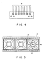
- Fig. 4 shows a state of the connection between the plurality of electrode pads 14 and the plurality of inner leads 19 formed on the TAB tape 17.
- a region in which slant lines are added shows the metal plating layer 20.
- each electrode pad 14 on the semiconductor chip 11 and each inner lead 19 are connected by the metal plating layer 20. Due to this, bonding capillary and TAB tool, which are used to the wire bonding and TAB connection are not required. Thereby, the distance between electrode pads 14 can be reduced to 100 ⁇ m or less, for example, about 50 ⁇ m.
- each electrode pad 14 and each inner lead 19 are electrically connected, no physical pressure is applied to the semiconductor chip 11, so that reliance due to pressure damage is not lowered. Then, since a large number of portions can be connected at the same time under the same condition, reliance of connection can be improved. Moreover, since there is no need of heating when the connection is performed, it is possible to prevent reliance from being lowered by thermal stress, which is caused by a mismatch of the coefficient of thermal expansion of each semiconductor layer in the semiconductor chip.
- TAB tape As shown in Fig. 5, metal foil such copper foil is laminated on the organic film material 18 in advance. Thereafter, in every semiconductor device, there are formed a plurality of lead electrodes 41 comprising the inner leads and the outer leads connected to the inner leads by the selection etching technique. At the same time when the selection etching is performed, common electrodes 42, which are electrically connected to the lead electrodes 41, are formed around each semiconductor device in a state that all common electrodes 42 are connected. Additionally, in Fig. 5, reference numeral 43 is an opening formed in the organic film material 18.
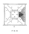
- Fig. 6 shows an enlarged one semiconductor device in the TAB tape of Fig. 5
- the semiconductor chip is adhered to TAB tape in a state that the semiconductor chip is positioned in the area shown by a one dotted chine line.
- the semiconductor chip is adhered to TAB tape so that the pad of each electrode on the semiconductor chip is positioned close to the portion where each end of the end portion of the plurality of leads is exposed.
- TAB tape is immersed in nickel plating bath together with a plating electrode.
- the nickel plating bath is generally called a watt bath, and nickel sulfate, nickel chloride, and adhesive are used.
- a predetermined direct voltage is applied between the common electrode 42 and the plating electrode in order that the common electrode 42 serves as a positive side and the plating electrode serves as a negative side, and electrolytic plating is performed for a predetermined period of time.
- a direct voltage to be applied was set to 2V
- a current to be supplied between the positive and negative sides was set to 60mA
- plating time was set to 10 minutes.
- metal plating layer 20 a nickel plating layer having a thickness of 10 ⁇ m was obtained as metal plating layer 20.
- the metal plating layer grows from each end surface of the top end portion of the inner lead immediately after plating starts. Then, if the growth advances and the plating layer contacts the electrode pad on the semiconductor chip, the metal layer also grows in the electrode pad, and both the common electrode 42 and the plating electrode are finally electrically connected by the plating layer. After the end of plating, the plating layer is washed with pure water, and contaminant, which was adhered to the surface when plating, is removed.
- each lead electrode 41 which comprises the inner and outer leads
- the most of the surface other than the top end portion of the inner lead is coated with an epoxy insulating film, which is called green coat.
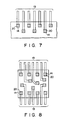
- the electrode pads were arranged in line with a predetermined distance.
- the electrode pads 14 are arranged on the semiconductor chip in a zig-zag manner.
- the same reference numerals as Fig. 4 are added in the portions corresponding to the portions of Fig. 4, and the explanation thereof is omitted.
- Fig. 8 shows a modification of the device using a semiconductor which is the so-called free access pad layout system wherein the electrode pads are arranged on the entire surface of the semiconductor chip at random.
- the present invention can be used in any type of chip regardless of the arrangement of the electrode pads on the chip.
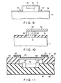
- Fig. 9 shows the structure of the semiconductor device relating to a second embodiment of the present invention wherein the present invention is used in the connection between the outer leads of the lead frame and the wiring pattern on the print circuit board.
- reference numeral 11 is a semiconductor chip
- reference numeral 17 is a TAB tape.
- the top end portion of the inner lead of the TAB tap and electrode pad (not shown) on the semiconductor chip 11 are electrically connected by a metal plating layer 20 similar to the first embodiment.
- a wiring pattern 52 which is formed on a print circuit board 51, and the outer lead of the TAB tape are also electrically connected by the metal plating layer 20.
- Fig. 10 shows the structure of the semiconductor device relating to a third embodiment of the present invention wherein the present invention is used in the connection between the outer leads of the lead frame and the wiring pattern on the print circuit board.
- the lead frame is formed by punching a metal thin film, which is formed of alloy such as 4-2 alloy and copper by a press process.
- An inner lead 53 of the lead frame and an electrode pad 14 on a semiconductor chip are electrically connected by use of both a conductive adhesive 54 and a metal plating layer 55.
- the metal plating layer can be formed in a manner that the semiconductor chip is adhered to the TAB tape by the adhesive in advance.
- the adhesive 54 is formed on each electrode pad 14 in advance by a screen printing method and the electrode pad 14 and the lead frame 53 are adhered by the adhesive 54. Thereafter, the plating layer 55 is formed by the same method as mentioned above, and both the electrode pad and the lead frame can be electrically connected.
- the present invention can be used in not only the connection between the inner lead of the lead frame and the electrode pad on the semiconductor chip but also the connection between the outer lead and the wiring pattern on the print circuit board, and the same effect can be obtained. Moreover, the present invention can be used in the electrical connection between a liquid crystal display and TAB tape.
- the present invention is not limited to the above-mentioned embodiments. It is needless to say that the present invention can be variously modified. For example, in the above embodiments explained the case wherein the metal plating layer was the nickel plating layer. According to the present invention, Au plating layer and copper plating layer can be used in addition to the above case.
- the above first embodiment explained the case wherein the most of the surface other than the top end portion of the inner lead was coated with the insulating film in advance.
- the thickness of which the plating layer can grow on the above portion is about only 1/10 times that of the top end portion when the electrolytic plating is performed, the adherence of the insulating film can be omitted.
- the method of the above embodiment explained the case that the plating layer was formed by the electrolytic plating method.
- the plating layer can be formed by an electrolessly plating method.
- Fig. 11 is a cross sectional view showing a device of a fourth embodiment of the present invention.
- the above embodiments explained the case in which two wirings are connected to each other by the plating metal.
- this plating metal can be used as a sealing for the semiconductor device.
- the device of the fourth embodiment shows that the plating layer is used as a sealing for a cap of a PGA (Pin Grid Array) typed semiconductor device.
- a package 61 is formed by layering tow ceramic plates 62 and 63. On one ceramic plate 62, a concave portion 64 is formed, and a semiconductor chip 65 is contained in the concave portion 64. Also, a plurality of wirings 66, 66, ... are formed on the surface of one ceramic plate 62.
- an opening 68 having an area larger than the concave portion 64 at the position corresponding to the concave portion 64 of one ceramic plate 62.
- the opening 68 forms the concave portion 64 and the containing section of the semiconductor chip 68.
- an Fe - Ni metal layer 69 on the surface of the ceramic plate 63 around the opening 68.
- the opening 68 of the ceramic plate 63 is covered with a cap 70.
- the metal layer 69 and the cap 70 are adhered to each other by a metal plating layer 71 formed of nickel.
- the metal plating layer 71 is also formed between the cap 70 and the metal layer 69 and on the entire exposed surface.
- the metal plating layer can be used as a sealing for the cap.
Landscapes
- Wire Bonding (AREA)
- Lead Frames For Integrated Circuits (AREA)
Priority Applications (1)
| Application Number | Priority Date | Filing Date | Title |
|---|---|---|---|
| EP00103351A EP1020903B1 (de) | 1990-06-01 | 1991-05-31 | Leiterrahmen für eine Halbleiteranordnung und dessen Herstellungsverfahren |
Applications Claiming Priority (3)
| Application Number | Priority Date | Filing Date | Title |
|---|---|---|---|
| JP141684/90 | 1990-06-01 | ||
| JP14168490 | 1990-06-01 | ||
| JP2141684A JP2540652B2 (ja) | 1990-06-01 | 1990-06-01 | 半導体装置 |
Related Child Applications (1)
| Application Number | Title | Priority Date | Filing Date |
|---|---|---|---|
| EP00103351A Division EP1020903B1 (de) | 1990-06-01 | 1991-05-31 | Leiterrahmen für eine Halbleiteranordnung und dessen Herstellungsverfahren |
Publications (3)
| Publication Number | Publication Date |
|---|---|
| EP0459493A2 true EP0459493A2 (de) | 1991-12-04 |
| EP0459493A3 EP0459493A3 (de) | 1994-02-23 |
| EP0459493B1 EP0459493B1 (de) | 2001-08-16 |
Family
ID=15297809
Family Applications (2)
| Application Number | Title | Priority Date | Filing Date |
|---|---|---|---|
| EP00103351A Expired - Lifetime EP1020903B1 (de) | 1990-06-01 | 1991-05-31 | Leiterrahmen für eine Halbleiteranordnung und dessen Herstellungsverfahren |
| EP91108886A Expired - Lifetime EP0459493B1 (de) | 1990-06-01 | 1991-05-31 | Halbleiteranordnung bestehend aus einem TAB-Band und deren Herstellungsverfahren |
Family Applications Before (1)
| Application Number | Title | Priority Date | Filing Date |
|---|---|---|---|
| EP00103351A Expired - Lifetime EP1020903B1 (de) | 1990-06-01 | 1991-05-31 | Leiterrahmen für eine Halbleiteranordnung und dessen Herstellungsverfahren |
Country Status (5)
| Country | Link |
|---|---|
| US (1) | US5654584A (de) |
| EP (2) | EP1020903B1 (de) |
| JP (1) | JP2540652B2 (de) |
| KR (1) | KR970000972B1 (de) |
| DE (2) | DE69133497T2 (de) |
Cited By (16)
| Publication number | Priority date | Publication date | Assignee | Title |
|---|---|---|---|---|
| GB2278956A (en) * | 1993-06-09 | 1994-12-14 | At & T Corp | Integrated circuit with multiple relative offset bond pad array |
| EP0684644A1 (de) * | 1994-05-25 | 1995-11-29 | Nec Corporation | Herstellungsverfahren einer mit Anschlusshöckern versehenen Halbleiteranordnung vom Filmträgertyp |
| EP0640245A4 (de) * | 1993-03-10 | 1995-12-13 | Atmel Corp | Höckerloses bondierungsverfahren einer mehrlagenmetallisierung. |
| CN1071493C (zh) * | 1995-10-19 | 2001-09-19 | Lg半导体株式会社 | 一种tab带和使用该tab带的半导体器件 |
| SG103824A1 (en) * | 1999-10-15 | 2004-05-26 | Amkor Technology Inc | Leadframe and semiconductor package with improved solder joint strength |
| US8154111B2 (en) | 1999-12-16 | 2012-04-10 | Amkor Technology, Inc. | Near chip size semiconductor package |
| US8866278B1 (en) | 2011-10-10 | 2014-10-21 | Amkor Technology, Inc. | Semiconductor device with increased I/O configuration |
| US9631481B1 (en) | 2011-01-27 | 2017-04-25 | Amkor Technology, Inc. | Semiconductor device including leadframe with a combination of leads and lands and method |
| US9673122B2 (en) | 2014-05-02 | 2017-06-06 | Amkor Technology, Inc. | Micro lead frame structure having reinforcing portions and method |
| US9691734B1 (en) | 2009-12-07 | 2017-06-27 | Amkor Technology, Inc. | Method of forming a plurality of electronic component packages |
| US9704725B1 (en) | 2012-03-06 | 2017-07-11 | Amkor Technology, Inc. | Semiconductor device with leadframe configured to facilitate reduced burr formation |
| US9871015B1 (en) | 2002-11-08 | 2018-01-16 | Amkor Technology, Inc. | Wafer level package and fabrication method |
| US9947623B1 (en) | 2011-11-29 | 2018-04-17 | Amkor Technology, Inc. | Semiconductor device comprising a conductive pad on a protruding-through electrode |
| CN107946201A (zh) * | 2017-12-19 | 2018-04-20 | 哈尔滨工业大学 | 一种基于局域电沉积的引线键合焊点结构的制备方法 |
| US10014240B1 (en) | 2012-03-29 | 2018-07-03 | Amkor Technology, Inc. | Embedded component package and fabrication method |
| US10811341B2 (en) | 2009-01-05 | 2020-10-20 | Amkor Technology Singapore Holding Pte Ltd. | Semiconductor device with through-mold via |
Families Citing this family (152)
| Publication number | Priority date | Publication date | Assignee | Title |
|---|---|---|---|---|
| JP3226752B2 (ja) * | 1995-04-12 | 2001-11-05 | 株式会社東芝 | 半導体装置の製造方法 |
| KR100186333B1 (ko) * | 1996-06-20 | 1999-03-20 | 문정환 | 칩 사이즈 반도체 패키지 및 그 제조방법 |
| SG75841A1 (en) | 1998-05-02 | 2000-10-24 | Eriston Invest Pte Ltd | Flip chip assembly with via interconnection |
| US6406939B1 (en) | 1998-05-02 | 2002-06-18 | Charles W. C. Lin | Flip chip assembly with via interconnection |
| US6143981A (en) | 1998-06-24 | 2000-11-07 | Amkor Technology, Inc. | Plastic integrated circuit package and method and leadframe for making the package |
| US7071541B1 (en) | 1998-06-24 | 2006-07-04 | Amkor Technology, Inc. | Plastic integrated circuit package and method and leadframe for making the package |
| US7030474B1 (en) | 1998-06-24 | 2006-04-18 | Amkor Technology, Inc. | Plastic integrated circuit package and method and leadframe for making the package |
| US7332375B1 (en) | 1998-06-24 | 2008-02-19 | Amkor Technology, Inc. | Method of making an integrated circuit package |
| US7112474B1 (en) | 1998-06-24 | 2006-09-26 | Amkor Technology, Inc. | Method of making an integrated circuit package |
| US7005326B1 (en) | 1998-06-24 | 2006-02-28 | Amkor Technology, Inc. | Method of making an integrated circuit package |
| US6893900B1 (en) | 1998-06-24 | 2005-05-17 | Amkor Technology, Inc. | Method of making an integrated circuit package |
| US6448633B1 (en) | 1998-11-20 | 2002-09-10 | Amkor Technology, Inc. | Semiconductor package and method of making using leadframe having lead locks to secure leads to encapsulant |
| TW444236B (en) | 1998-12-17 | 2001-07-01 | Charles Wen Chyang Lin | Bumpless flip chip assembly with strips and via-fill |
| TW522536B (en) | 1998-12-17 | 2003-03-01 | Wen-Chiang Lin | Bumpless flip chip assembly with strips-in-via and plating |
| TW396462B (en) | 1998-12-17 | 2000-07-01 | Eriston Technologies Pte Ltd | Bumpless flip chip assembly with solder via |
| KR100403142B1 (ko) | 1999-10-15 | 2003-10-30 | 앰코 테크놀로지 코리아 주식회사 | 반도체패키지 |
| KR20010037247A (ko) | 1999-10-15 | 2001-05-07 | 마이클 디. 오브라이언 | 반도체패키지 |
| US6580159B1 (en) | 1999-11-05 | 2003-06-17 | Amkor Technology, Inc. | Integrated circuit device packages and substrates for making the packages |
| US6847103B1 (en) | 1999-11-09 | 2005-01-25 | Amkor Technology, Inc. | Semiconductor package with exposed die pad and body-locking leadframe |
| KR100421774B1 (ko) | 1999-12-16 | 2004-03-10 | 앰코 테크놀로지 코리아 주식회사 | 반도체패키지 및 그 제조 방법 |
| KR100583494B1 (ko) | 2000-03-25 | 2006-05-24 | 앰코 테크놀로지 코리아 주식회사 | 반도체패키지 |
| US7042068B2 (en) | 2000-04-27 | 2006-05-09 | Amkor Technology, Inc. | Leadframe and semiconductor package made using the leadframe |
| US6350633B1 (en) | 2000-08-22 | 2002-02-26 | Charles W. C. Lin | Semiconductor chip assembly with simultaneously electroplated contact terminal and connection joint |
| US6660626B1 (en) | 2000-08-22 | 2003-12-09 | Charles W. C. Lin | Semiconductor chip assembly with simultaneously electrolessly plated contact terminal and connection joint |
| US6562709B1 (en) | 2000-08-22 | 2003-05-13 | Charles W. C. Lin | Semiconductor chip assembly with simultaneously electroplated contact terminal and connection joint |
| US6551861B1 (en) | 2000-08-22 | 2003-04-22 | Charles W. C. Lin | Method of making a semiconductor chip assembly by joining the chip to a support circuit with an adhesive |
| US6436734B1 (en) | 2000-08-22 | 2002-08-20 | Charles W. C. Lin | Method of making a support circuit for a semiconductor chip assembly |
| US6402970B1 (en) | 2000-08-22 | 2002-06-11 | Charles W. C. Lin | Method of making a support circuit for a semiconductor chip assembly |
| US6403460B1 (en) | 2000-08-22 | 2002-06-11 | Charles W. C. Lin | Method of making a semiconductor chip assembly |
| US6562657B1 (en) | 2000-08-22 | 2003-05-13 | Charles W. C. Lin | Semiconductor chip assembly with simultaneously electrolessly plated contact terminal and connection joint |
| US6350632B1 (en) | 2000-09-20 | 2002-02-26 | Charles W. C. Lin | Semiconductor chip assembly with ball bond connection joint |
| US6511865B1 (en) | 2000-09-20 | 2003-01-28 | Charles W. C. Lin | Method for forming a ball bond connection joint on a conductive trace and conductive pad in a semiconductor chip assembly |
| US6350386B1 (en) | 2000-09-20 | 2002-02-26 | Charles W. C. Lin | Method of making a support circuit with a tapered through-hole for a semiconductor chip assembly |
| US6544813B1 (en) | 2000-10-02 | 2003-04-08 | Charles W. C. Lin | Method of making a semiconductor chip assembly with a conductive trace subtractively formed before and after chip attachment |
| US6448108B1 (en) | 2000-10-02 | 2002-09-10 | Charles W. C. Lin | Method of making a semiconductor chip assembly with a conductive trace subtractively formed before and after chip attachment |
| US7129575B1 (en) | 2000-10-13 | 2006-10-31 | Bridge Semiconductor Corporation | Semiconductor chip assembly with bumped metal pillar |
| US7009297B1 (en) | 2000-10-13 | 2006-03-07 | Bridge Semiconductor Corporation | Semiconductor chip assembly with embedded metal particle |
| US6908788B1 (en) | 2000-10-13 | 2005-06-21 | Bridge Semiconductor Corporation | Method of connecting a conductive trace to a semiconductor chip using a metal base |
| US6537851B1 (en) | 2000-10-13 | 2003-03-25 | Bridge Semiconductor Corporation | Method of connecting a bumped compliant conductive trace to a semiconductor chip |
| US6984576B1 (en) | 2000-10-13 | 2006-01-10 | Bridge Semiconductor Corporation | Method of connecting an additively and subtractively formed conductive trace and an insulative base to a semiconductor chip |
| US6576493B1 (en) | 2000-10-13 | 2003-06-10 | Bridge Semiconductor Corporation | Method of connecting a conductive trace and an insulative base to a semiconductor chip using multiple etch steps |
| US7414319B2 (en) * | 2000-10-13 | 2008-08-19 | Bridge Semiconductor Corporation | Semiconductor chip assembly with metal containment wall and solder terminal |
| US7132741B1 (en) | 2000-10-13 | 2006-11-07 | Bridge Semiconductor Corporation | Semiconductor chip assembly with carved bumped terminal |
| US7190080B1 (en) | 2000-10-13 | 2007-03-13 | Bridge Semiconductor Corporation | Semiconductor chip assembly with embedded metal pillar |
| US7319265B1 (en) | 2000-10-13 | 2008-01-15 | Bridge Semiconductor Corporation | Semiconductor chip assembly with precision-formed metal pillar |
| US6440835B1 (en) | 2000-10-13 | 2002-08-27 | Charles W. C. Lin | Method of connecting a conductive trace to a semiconductor chip |
| US6673710B1 (en) | 2000-10-13 | 2004-01-06 | Bridge Semiconductor Corporation | Method of connecting a conductive trace and an insulative base to a semiconductor chip |
| US6576539B1 (en) | 2000-10-13 | 2003-06-10 | Charles W.C. Lin | Semiconductor chip assembly with interlocked conductive trace |
| US7094676B1 (en) | 2000-10-13 | 2006-08-22 | Bridge Semiconductor Corporation | Semiconductor chip assembly with embedded metal pillar |
| US6667229B1 (en) | 2000-10-13 | 2003-12-23 | Bridge Semiconductor Corporation | Method of connecting a bumped compliant conductive trace and an insulative base to a semiconductor chip |
| US6699780B1 (en) | 2000-10-13 | 2004-03-02 | Bridge Semiconductor Corporation | Method of connecting a conductive trace to a semiconductor chip using plasma undercut etching |
| US6492252B1 (en) | 2000-10-13 | 2002-12-10 | Bridge Semiconductor Corporation | Method of connecting a bumped conductive trace to a semiconductor chip |
| US6872591B1 (en) | 2000-10-13 | 2005-03-29 | Bridge Semiconductor Corporation | Method of making a semiconductor chip assembly with a conductive trace and a substrate |
| US7075186B1 (en) | 2000-10-13 | 2006-07-11 | Bridge Semiconductor Corporation | Semiconductor chip assembly with interlocked contact terminal |
| US7262082B1 (en) | 2000-10-13 | 2007-08-28 | Bridge Semiconductor Corporation | Method of making a three-dimensional stacked semiconductor package with a metal pillar and a conductive interconnect in an encapsulant aperture |
| US6548393B1 (en) | 2000-10-13 | 2003-04-15 | Charles W. C. Lin | Semiconductor chip assembly with hardened connection joint |
| US7071089B1 (en) | 2000-10-13 | 2006-07-04 | Bridge Semiconductor Corporation | Method of making a semiconductor chip assembly with a carved bumped terminal |
| US7129113B1 (en) | 2000-10-13 | 2006-10-31 | Bridge Semiconductor Corporation | Method of making a three-dimensional stacked semiconductor package with a metal pillar in an encapsulant aperture |
| US7264991B1 (en) | 2000-10-13 | 2007-09-04 | Bridge Semiconductor Corporation | Method of connecting a conductive trace to a semiconductor chip using conductive adhesive |
| US6740576B1 (en) | 2000-10-13 | 2004-05-25 | Bridge Semiconductor Corporation | Method of making a contact terminal with a plated metal peripheral sidewall portion for a semiconductor chip assembly |
| US6949408B1 (en) | 2000-10-13 | 2005-09-27 | Bridge Semiconductor Corporation | Method of connecting a conductive trace and an insulative base to a semiconductor chip using multiple etch steps |
| US6876072B1 (en) | 2000-10-13 | 2005-04-05 | Bridge Semiconductor Corporation | Semiconductor chip assembly with chip in substrate cavity |
| US6444489B1 (en) | 2000-12-15 | 2002-09-03 | Charles W. C. Lin | Semiconductor chip assembly with bumped molded substrate |
| KR20020058209A (ko) | 2000-12-29 | 2002-07-12 | 마이클 디. 오브라이언 | 반도체패키지 |
| US6653170B1 (en) | 2001-02-06 | 2003-11-25 | Charles W. C. Lin | Semiconductor chip assembly with elongated wire ball bonded to chip and electrolessly plated to support circuit |
| US6967395B1 (en) | 2001-03-20 | 2005-11-22 | Amkor Technology, Inc. | Mounting for a package containing a chip |
| KR100369393B1 (ko) | 2001-03-27 | 2003-02-05 | 앰코 테크놀로지 코리아 주식회사 | 리드프레임 및 이를 이용한 반도체패키지와 그 제조 방법 |
| KR100393448B1 (ko) | 2001-03-27 | 2003-08-02 | 앰코 테크놀로지 코리아 주식회사 | 반도체 패키지 및 그 제조 방법 |
| US7045883B1 (en) | 2001-04-04 | 2006-05-16 | Amkor Technology, Inc. | Thermally enhanced chip scale lead on chip semiconductor package and method of making same |
| US7064009B1 (en) | 2001-04-04 | 2006-06-20 | Amkor Technology, Inc. | Thermally enhanced chip scale lead on chip semiconductor package and method of making same |
| US6597059B1 (en) | 2001-04-04 | 2003-07-22 | Amkor Technology, Inc. | Thermally enhanced chip scale lead on chip semiconductor package |
| US7485952B1 (en) | 2001-09-19 | 2009-02-03 | Amkor Technology, Inc. | Drop resistant bumpers for fully molded memory cards |
| US6900527B1 (en) | 2001-09-19 | 2005-05-31 | Amkor Technology, Inc. | Lead-frame method and assembly for interconnecting circuits within a circuit module |
| US6630726B1 (en) | 2001-11-07 | 2003-10-07 | Amkor Technology, Inc. | Power semiconductor package with strap |
| US6608366B1 (en) | 2002-04-15 | 2003-08-19 | Harry J. Fogelson | Lead frame with plated end leads |
| US6818973B1 (en) | 2002-09-09 | 2004-11-16 | Amkor Technology, Inc. | Exposed lead QFP package fabricated through the use of a partial saw process |
| US7361533B1 (en) | 2002-11-08 | 2008-04-22 | Amkor Technology, Inc. | Stacked embedded leadframe |
| US7723210B2 (en) | 2002-11-08 | 2010-05-25 | Amkor Technology, Inc. | Direct-write wafer level chip scale package |
| US7190062B1 (en) | 2004-06-15 | 2007-03-13 | Amkor Technology, Inc. | Embedded leadframe semiconductor package |
| US6847099B1 (en) | 2003-02-05 | 2005-01-25 | Amkor Technology Inc. | Offset etched corner leads for semiconductor package |
| US6794740B1 (en) | 2003-03-13 | 2004-09-21 | Amkor Technology, Inc. | Leadframe package for semiconductor devices |
| US7001799B1 (en) | 2003-03-13 | 2006-02-21 | Amkor Technology, Inc. | Method of making a leadframe for semiconductor devices |
| US6879034B1 (en) | 2003-05-01 | 2005-04-12 | Amkor Technology, Inc. | Semiconductor package including low temperature co-fired ceramic substrate |
| US7008825B1 (en) | 2003-05-27 | 2006-03-07 | Amkor Technology, Inc. | Leadframe strip having enhanced testability |
| US6897550B1 (en) | 2003-06-11 | 2005-05-24 | Amkor Technology, Inc. | Fully-molded leadframe stand-off feature |
| US7245007B1 (en) | 2003-09-18 | 2007-07-17 | Amkor Technology, Inc. | Exposed lead interposer leadframe package |
| US6921967B2 (en) | 2003-09-24 | 2005-07-26 | Amkor Technology, Inc. | Reinforced die pad support structure |
| US7138707B1 (en) | 2003-10-21 | 2006-11-21 | Amkor Technology, Inc. | Semiconductor package including leads and conductive posts for providing increased functionality |
| US7144517B1 (en) | 2003-11-07 | 2006-12-05 | Amkor Technology, Inc. | Manufacturing method for leadframe and for semiconductor package using the leadframe |
| US7211879B1 (en) | 2003-11-12 | 2007-05-01 | Amkor Technology, Inc. | Semiconductor package with chamfered corners and method of manufacturing the same |
| US7993983B1 (en) | 2003-11-17 | 2011-08-09 | Bridge Semiconductor Corporation | Method of making a semiconductor chip assembly with chip and encapsulant grinding |
| US7425759B1 (en) | 2003-11-20 | 2008-09-16 | Bridge Semiconductor Corporation | Semiconductor chip assembly with bumped terminal and filler |
| US7538415B1 (en) | 2003-11-20 | 2009-05-26 | Bridge Semiconductor Corporation | Semiconductor chip assembly with bumped terminal, filler and insulative base |
| US7057268B1 (en) | 2004-01-27 | 2006-06-06 | Amkor Technology, Inc. | Cavity case with clip/plug for use on multi-media card |
| US7091594B1 (en) | 2004-01-28 | 2006-08-15 | Amkor Technology, Inc. | Leadframe type semiconductor package having reduced inductance and its manufacturing method |
| US7202554B1 (en) | 2004-08-19 | 2007-04-10 | Amkor Technology, Inc. | Semiconductor package and its manufacturing method |
| US7761814B2 (en) | 2004-09-13 | 2010-07-20 | Microsoft Corporation | Flick gesture |
| US7217991B1 (en) | 2004-10-22 | 2007-05-15 | Amkor Technology, Inc. | Fan-in leadframe semiconductor package |
| US7268421B1 (en) | 2004-11-10 | 2007-09-11 | Bridge Semiconductor Corporation | Semiconductor chip assembly with welded metal pillar that includes enlarged ball bond |
| US7446419B1 (en) | 2004-11-10 | 2008-11-04 | Bridge Semiconductor Corporation | Semiconductor chip assembly with welded metal pillar of stacked metal balls |
| US7750483B1 (en) | 2004-11-10 | 2010-07-06 | Bridge Semiconductor Corporation | Semiconductor chip assembly with welded metal pillar and enlarged plated contact terminal |
| US7507603B1 (en) | 2005-12-02 | 2009-03-24 | Amkor Technology, Inc. | Etch singulated semiconductor package |
| US7572681B1 (en) | 2005-12-08 | 2009-08-11 | Amkor Technology, Inc. | Embedded electronic component package |
| US7902660B1 (en) | 2006-05-24 | 2011-03-08 | Amkor Technology, Inc. | Substrate for semiconductor device and manufacturing method thereof |
| US7968998B1 (en) | 2006-06-21 | 2011-06-28 | Amkor Technology, Inc. | Side leaded, bottom exposed pad and bottom exposed lead fusion quad flat semiconductor package |
| JP2008078561A (ja) * | 2006-09-25 | 2008-04-03 | Toshiba Corp | 半導体装置及びその製造方法 |
| US7494843B1 (en) | 2006-12-26 | 2009-02-24 | Bridge Semiconductor Corporation | Method of making a semiconductor chip assembly with thermal conductor and encapsulant grinding |
| US7811863B1 (en) | 2006-10-26 | 2010-10-12 | Bridge Semiconductor Corporation | Method of making a semiconductor chip assembly with metal pillar and encapsulant grinding and heat sink attachment |
| US7687893B2 (en) | 2006-12-27 | 2010-03-30 | Amkor Technology, Inc. | Semiconductor package having leadframe with exposed anchor pads |
| US7829990B1 (en) | 2007-01-18 | 2010-11-09 | Amkor Technology, Inc. | Stackable semiconductor package including laminate interposer |
| US7982297B1 (en) | 2007-03-06 | 2011-07-19 | Amkor Technology, Inc. | Stackable semiconductor package having partially exposed semiconductor die and method of fabricating the same |
| US7977774B2 (en) | 2007-07-10 | 2011-07-12 | Amkor Technology, Inc. | Fusion quad flat semiconductor package |
| US7687899B1 (en) | 2007-08-07 | 2010-03-30 | Amkor Technology, Inc. | Dual laminate package structure with embedded elements |
| US7777351B1 (en) | 2007-10-01 | 2010-08-17 | Amkor Technology, Inc. | Thin stacked interposer package |
| US8089159B1 (en) | 2007-10-03 | 2012-01-03 | Amkor Technology, Inc. | Semiconductor package with increased I/O density and method of making the same |
| US7847386B1 (en) | 2007-11-05 | 2010-12-07 | Amkor Technology, Inc. | Reduced size stacked semiconductor package and method of making the same |
| US7956453B1 (en) | 2008-01-16 | 2011-06-07 | Amkor Technology, Inc. | Semiconductor package with patterning layer and method of making same |
| US7723852B1 (en) | 2008-01-21 | 2010-05-25 | Amkor Technology, Inc. | Stacked semiconductor package and method of making same |
| US8067821B1 (en) | 2008-04-10 | 2011-11-29 | Amkor Technology, Inc. | Flat semiconductor package with half package molding |
| US7768135B1 (en) | 2008-04-17 | 2010-08-03 | Amkor Technology, Inc. | Semiconductor package with fast power-up cycle and method of making same |
| US7808084B1 (en) | 2008-05-06 | 2010-10-05 | Amkor Technology, Inc. | Semiconductor package with half-etched locking features |
| US8125064B1 (en) | 2008-07-28 | 2012-02-28 | Amkor Technology, Inc. | Increased I/O semiconductor package and method of making same |
| US8184453B1 (en) | 2008-07-31 | 2012-05-22 | Amkor Technology, Inc. | Increased capacity semiconductor package |
| US7847392B1 (en) | 2008-09-30 | 2010-12-07 | Amkor Technology, Inc. | Semiconductor device including leadframe with increased I/O |
| US7989933B1 (en) | 2008-10-06 | 2011-08-02 | Amkor Technology, Inc. | Increased I/O leadframe and semiconductor device including same |
| US8008758B1 (en) | 2008-10-27 | 2011-08-30 | Amkor Technology, Inc. | Semiconductor device with increased I/O leadframe |
| US8089145B1 (en) | 2008-11-17 | 2012-01-03 | Amkor Technology, Inc. | Semiconductor device including increased capacity leadframe |
| US8072050B1 (en) | 2008-11-18 | 2011-12-06 | Amkor Technology, Inc. | Semiconductor device with increased I/O leadframe including passive device |
| US7875963B1 (en) | 2008-11-21 | 2011-01-25 | Amkor Technology, Inc. | Semiconductor device including leadframe having power bars and increased I/O |
| US7982298B1 (en) | 2008-12-03 | 2011-07-19 | Amkor Technology, Inc. | Package in package semiconductor device |
| US8680656B1 (en) | 2009-01-05 | 2014-03-25 | Amkor Technology, Inc. | Leadframe structure for concentrated photovoltaic receiver package |
| US8058715B1 (en) | 2009-01-09 | 2011-11-15 | Amkor Technology, Inc. | Package in package device for RF transceiver module |
| US8026589B1 (en) | 2009-02-23 | 2011-09-27 | Amkor Technology, Inc. | Reduced profile stackable semiconductor package |
| US7960818B1 (en) | 2009-03-04 | 2011-06-14 | Amkor Technology, Inc. | Conformal shield on punch QFN semiconductor package |
| US8575742B1 (en) | 2009-04-06 | 2013-11-05 | Amkor Technology, Inc. | Semiconductor device with increased I/O leadframe including power bars |
| US8796561B1 (en) | 2009-10-05 | 2014-08-05 | Amkor Technology, Inc. | Fan out build up substrate stackable package and method |
| US8937381B1 (en) | 2009-12-03 | 2015-01-20 | Amkor Technology, Inc. | Thin stackable package and method |
| US8324511B1 (en) | 2010-04-06 | 2012-12-04 | Amkor Technology, Inc. | Through via nub reveal method and structure |
| US8294276B1 (en) | 2010-05-27 | 2012-10-23 | Amkor Technology, Inc. | Semiconductor device and fabricating method thereof |
| US8440554B1 (en) | 2010-08-02 | 2013-05-14 | Amkor Technology, Inc. | Through via connected backside embedded circuit features structure and method |
| US8487445B1 (en) | 2010-10-05 | 2013-07-16 | Amkor Technology, Inc. | Semiconductor device having through electrodes protruding from dielectric layer |
| US8791501B1 (en) | 2010-12-03 | 2014-07-29 | Amkor Technology, Inc. | Integrated passive device structure and method |
| US8674485B1 (en) | 2010-12-08 | 2014-03-18 | Amkor Technology, Inc. | Semiconductor device including leadframe with downsets |
| US8390130B1 (en) | 2011-01-06 | 2013-03-05 | Amkor Technology, Inc. | Through via recessed reveal structure and method |
| US8648450B1 (en) | 2011-01-27 | 2014-02-11 | Amkor Technology, Inc. | Semiconductor device including leadframe with a combination of leads and lands |
| US9048298B1 (en) | 2012-03-29 | 2015-06-02 | Amkor Technology, Inc. | Backside warpage control structure and fabrication method |
| JP2013138511A (ja) * | 2013-03-27 | 2013-07-11 | Taiyo Yuden Co Ltd | 弾性波装置 |
| KR101486790B1 (ko) | 2013-05-02 | 2015-01-28 | 앰코 테크놀로지 코리아 주식회사 | 강성보강부를 갖는 마이크로 리드프레임 |
| US20150075849A1 (en) * | 2013-09-17 | 2015-03-19 | Jia Lin Yap | Semiconductor device and lead frame with interposer |
| KR101563911B1 (ko) | 2013-10-24 | 2015-10-28 | 앰코 테크놀로지 코리아 주식회사 | 반도체 패키지 |
| CN108054108B (zh) * | 2017-12-19 | 2019-10-25 | 哈尔滨工业大学 | 一种基于快速局域电沉积的引线键合方法 |
| KR102646637B1 (ko) * | 2022-12-07 | 2024-03-12 | 주식회사바텍 | 엑스선 소스용 전압변환장치 |
Family Cites Families (29)
| Publication number | Priority date | Publication date | Assignee | Title |
|---|---|---|---|---|
| JPS53103659U (de) * | 1977-01-25 | 1978-08-21 | ||
| US4176443A (en) * | 1977-03-08 | 1979-12-04 | Sgs-Ates Componenti Elettronici S.P.A. | Method of connecting semiconductor structure to external circuits |
| JPS5524479A (en) * | 1978-08-09 | 1980-02-21 | Nec Corp | Semiconductor |
| JPS5750056A (en) * | 1980-09-09 | 1982-03-24 | Toshiba Corp | Information processor having branch trace function |
| JPS57143848A (en) * | 1981-02-27 | 1982-09-06 | Nec Corp | Semiconductor device |
| US4496965A (en) * | 1981-05-18 | 1985-01-29 | Texas Instruments Incorporated | Stacked interdigitated lead frame assembly |
| JPS6092636A (ja) * | 1983-10-27 | 1985-05-24 | Toshiba Corp | 半導体装置の製造方法 |
| JPS60115247A (ja) * | 1983-11-28 | 1985-06-21 | Fujitsu Ltd | 半導体装置 |
| JPS61208245A (ja) * | 1985-03-13 | 1986-09-16 | Kyushu Hitachi Maxell Ltd | 半導体装置のリ−ドフレ−ム製造方法 |
| JPS62108534A (ja) * | 1985-11-06 | 1987-05-19 | Nec Corp | 半導体装置 |
| US4977441A (en) * | 1985-12-25 | 1990-12-11 | Hitachi, Ltd. | Semiconductor device and tape carrier |
| JPH0682705B2 (ja) * | 1986-03-10 | 1994-10-19 | 株式会社東芝 | 半導体装置の実装方法 |
| JPS62296431A (ja) * | 1986-06-17 | 1987-12-23 | Alps Electric Co Ltd | フリツプチツプの接続方法 |
| JPS6373644A (ja) * | 1986-09-17 | 1988-04-04 | Fujitsu Ltd | 半導体装置の製造方法 |
| US4885630A (en) * | 1986-10-27 | 1989-12-05 | Electric Power Research Institute | High power multi-layer semiconductive switching device having multiple parallel contacts with improved forward voltage drop |
| US4839713A (en) * | 1987-02-20 | 1989-06-13 | Mitsubishi Denki Kabushiki Kaisha | Package structure for semiconductor device |
| JP2623578B2 (ja) * | 1987-07-14 | 1997-06-25 | 日本電気株式会社 | 半導体集積回路装置 |
| JPS6473734A (en) * | 1987-09-16 | 1989-03-20 | Nec Corp | Tape carrier |
| JPH01207938A (ja) * | 1988-02-15 | 1989-08-21 | Nec Corp | 半導体装置 |
| JPH01276750A (ja) * | 1988-04-28 | 1989-11-07 | Matsushita Electric Ind Co Ltd | 半導体装置 |
| JPH0233929A (ja) * | 1988-07-23 | 1990-02-05 | Nec Corp | 半導体装置 |
| JPH0266953A (ja) * | 1988-08-31 | 1990-03-07 | Nec Corp | 半導体素子の実装構造およびその製造方法 |
| US5016082A (en) * | 1988-09-16 | 1991-05-14 | Delco Electronics Corporation | Integrated circuit interconnect design |
| JPH0287538A (ja) * | 1988-09-26 | 1990-03-28 | Hitachi Ltd | テープキャリアモジュール |
| JP2651608B2 (ja) * | 1988-10-28 | 1997-09-10 | イビデン株式会社 | 電子部品搭載用基板 |
| JPH02119252A (ja) * | 1988-10-28 | 1990-05-07 | Nec Corp | 混成集積回路装置 |
| US4922322A (en) * | 1989-02-09 | 1990-05-01 | National Semiconductor Corporation | Bump structure for reflow bonding of IC devices |
| JPH02208957A (ja) * | 1989-02-09 | 1990-08-20 | Toshiba Corp | 電子機器用封着材料 |
| US4948645A (en) * | 1989-08-01 | 1990-08-14 | Rogers Corporation | Tape automated bonding and method of making the same |
-
1990
- 1990-06-01 JP JP2141684A patent/JP2540652B2/ja not_active Expired - Fee Related
-
1991
- 1991-05-31 EP EP00103351A patent/EP1020903B1/de not_active Expired - Lifetime
- 1991-05-31 DE DE69133497T patent/DE69133497T2/de not_active Expired - Fee Related
- 1991-05-31 DE DE69132685T patent/DE69132685T2/de not_active Expired - Fee Related
- 1991-05-31 KR KR1019910009041A patent/KR970000972B1/ko not_active Expired - Fee Related
- 1991-05-31 EP EP91108886A patent/EP0459493B1/de not_active Expired - Lifetime
-
1994
- 1994-11-18 US US08/344,605 patent/US5654584A/en not_active Expired - Fee Related
Cited By (29)
| Publication number | Priority date | Publication date | Assignee | Title |
|---|---|---|---|---|
| EP0640245A4 (de) * | 1993-03-10 | 1995-12-13 | Atmel Corp | Höckerloses bondierungsverfahren einer mehrlagenmetallisierung. |
| GB2278956A (en) * | 1993-06-09 | 1994-12-14 | At & T Corp | Integrated circuit with multiple relative offset bond pad array |
| GB2278956B (en) * | 1993-06-09 | 1997-10-08 | At & T Corp | Integrated circuit with multiple relative offset bond pad array |
| EP0684644A1 (de) * | 1994-05-25 | 1995-11-29 | Nec Corporation | Herstellungsverfahren einer mit Anschlusshöckern versehenen Halbleiteranordnung vom Filmträgertyp |
| US5683942A (en) * | 1994-05-25 | 1997-11-04 | Nec Corporation | Method for manufacturing bump leaded film carrier type semiconductor device |
| US5905303A (en) * | 1994-05-25 | 1999-05-18 | Nec Corporation | Method for manufacturing bump leaded film carrier type semiconductor device |
| EP0959499A1 (de) * | 1994-05-25 | 1999-11-24 | Nec Corporation | Herstellungsverfahren einer mit Anschlusshöckern versehenen Halbleiteranordnung vom Filmträgertyp |
| CN1071493C (zh) * | 1995-10-19 | 2001-09-19 | Lg半导体株式会社 | 一种tab带和使用该tab带的半导体器件 |
| SG103824A1 (en) * | 1999-10-15 | 2004-05-26 | Amkor Technology Inc | Leadframe and semiconductor package with improved solder joint strength |
| US7102208B1 (en) | 1999-10-15 | 2006-09-05 | Amkor Technology, Inc. | Leadframe and semiconductor package with improved solder joint strength |
| US8154111B2 (en) | 1999-12-16 | 2012-04-10 | Amkor Technology, Inc. | Near chip size semiconductor package |
| US9871015B1 (en) | 2002-11-08 | 2018-01-16 | Amkor Technology, Inc. | Wafer level package and fabrication method |
| US10665567B1 (en) | 2002-11-08 | 2020-05-26 | Amkor Technology, Inc. | Wafer level package and fabrication method |
| US12494414B2 (en) | 2009-01-05 | 2025-12-09 | Amkor Technology Singapore Holding Pte. Ltd. | Semiconductor device with through-mold via |
| US11869829B2 (en) | 2009-01-05 | 2024-01-09 | Amkor Technology Singapore Holding Pte. Ltd. | Semiconductor device with through-mold via |
| US10811341B2 (en) | 2009-01-05 | 2020-10-20 | Amkor Technology Singapore Holding Pte Ltd. | Semiconductor device with through-mold via |
| US9691734B1 (en) | 2009-12-07 | 2017-06-27 | Amkor Technology, Inc. | Method of forming a plurality of electronic component packages |
| US10546833B2 (en) | 2009-12-07 | 2020-01-28 | Amkor Technology, Inc. | Method of forming a plurality of electronic component packages |
| US9978695B1 (en) | 2011-01-27 | 2018-05-22 | Amkor Technology, Inc. | Semiconductor device including leadframe with a combination of leads and lands and method |
| US9631481B1 (en) | 2011-01-27 | 2017-04-25 | Amkor Technology, Inc. | Semiconductor device including leadframe with a combination of leads and lands and method |
| US8866278B1 (en) | 2011-10-10 | 2014-10-21 | Amkor Technology, Inc. | Semiconductor device with increased I/O configuration |
| US9947623B1 (en) | 2011-11-29 | 2018-04-17 | Amkor Technology, Inc. | Semiconductor device comprising a conductive pad on a protruding-through electrode |
| US10410967B1 (en) | 2011-11-29 | 2019-09-10 | Amkor Technology, Inc. | Electronic device comprising a conductive pad on a protruding-through electrode |
| US11043458B2 (en) | 2011-11-29 | 2021-06-22 | Amkor Technology Singapore Holding Pte. Ltd. | Method of manufacturing an electronic device comprising a conductive pad on a protruding-through electrode |
| US10090228B1 (en) | 2012-03-06 | 2018-10-02 | Amkor Technology, Inc. | Semiconductor device with leadframe configured to facilitate reduced burr formation |
| US9704725B1 (en) | 2012-03-06 | 2017-07-11 | Amkor Technology, Inc. | Semiconductor device with leadframe configured to facilitate reduced burr formation |
| US10014240B1 (en) | 2012-03-29 | 2018-07-03 | Amkor Technology, Inc. | Embedded component package and fabrication method |
| US9673122B2 (en) | 2014-05-02 | 2017-06-06 | Amkor Technology, Inc. | Micro lead frame structure having reinforcing portions and method |
| CN107946201A (zh) * | 2017-12-19 | 2018-04-20 | 哈尔滨工业大学 | 一种基于局域电沉积的引线键合焊点结构的制备方法 |
Also Published As
| Publication number | Publication date |
|---|---|
| DE69132685D1 (de) | 2001-09-20 |
| EP1020903B1 (de) | 2005-12-14 |
| EP1020903A1 (de) | 2000-07-19 |
| DE69133497D1 (de) | 2006-01-19 |
| EP0459493A3 (de) | 1994-02-23 |
| US5654584A (en) | 1997-08-05 |
| JP2540652B2 (ja) | 1996-10-09 |
| EP0459493B1 (de) | 2001-08-16 |
| KR920001701A (ko) | 1992-01-30 |
| KR970000972B1 (ko) | 1997-01-21 |
| DE69133497T2 (de) | 2006-08-24 |
| JPH0437149A (ja) | 1992-02-07 |
| DE69132685T2 (de) | 2002-06-13 |
Similar Documents
| Publication | Publication Date | Title |
|---|---|---|
| US5556810A (en) | Method for manufacturing a semiconductor device wherein a semiconductor chip is connected to a lead frame by metal plating | |
| EP0459493A2 (de) | Leiterrahmen für eine Halbleiteranordnung und dessen Herstellungsverfahren | |
| US4974057A (en) | Semiconductor device package with circuit board and resin | |
| US5892273A (en) | Semiconductor package integral with semiconductor chip | |
| US6744122B1 (en) | Semiconductor device, method of manufacture thereof, circuit board, and electronic device | |
| KR100541649B1 (ko) | 테이프 배선 기판과 그를 이용한 반도체 칩 패키지 | |
| US6420787B1 (en) | Semiconductor device and process of producing same | |
| US8067698B2 (en) | Wiring substrate for use in semiconductor apparatus, method for fabricating the same, and semiconductor apparatus using the same | |
| KR100620212B1 (ko) | 반도체 장치의 전기 전도체 시스템 및 그 제조 방법 | |
| JPH08293529A (ja) | 半導体装置およびその製造方法およびそれを用いた電子装置 | |
| US5528078A (en) | Film carrier and a method for manufacturing the same | |
| JP2005183868A (ja) | 半導体装置およびその実装構造 | |
| JPH06177315A (ja) | 多層リードフレーム | |
| JP4038021B2 (ja) | 半導体装置の製造方法 | |
| KR970005715B1 (ko) | 반도체 장치 및 그 제조 방법 | |
| EP0526147B1 (de) | Halbleiteranordnung vom Filmträgertyp und Verfahren zum Herstellen derselben | |
| JP2974840B2 (ja) | 半導体素子の実装方法 | |
| JP2736247B2 (ja) | 半導体装置の製造方法 | |
| JP2777345B2 (ja) | 半導体装置 | |
| KR100246848B1 (ko) | 랜드 그리드 어레이 및 이를 채용한 반도체 패키지 | |
| JP3214507B2 (ja) | 電子部品、電子回路素子搭載用基板及びその製造方法 | |
| JP2652222B2 (ja) | 電子部品搭載用基板 | |
| JPH11297740A (ja) | 半導体チップが実装されるキャリアテープ、および半導体装置 | |
| JP3053935B2 (ja) | 半導体装置及びその製造方法 | |
| JPS6237888B2 (de) |
Legal Events
| Date | Code | Title | Description |
|---|---|---|---|
| PUAI | Public reference made under article 153(3) epc to a published international application that has entered the european phase |
Free format text: ORIGINAL CODE: 0009012 |
|
| 17P | Request for examination filed |
Effective date: 19910531 |
|
| AK | Designated contracting states |
Kind code of ref document: A2 Designated state(s): DE FR GB |
|
| PUAL | Search report despatched |
Free format text: ORIGINAL CODE: 0009013 |
|
| AK | Designated contracting states |
Kind code of ref document: A3 Designated state(s): DE FR GB |
|
| 17Q | First examination report despatched |
Effective date: 19950224 |
|
| RTI1 | Title (correction) |
Free format text: A SEMICONDUCTOR DEVICE COMPRISING A TAB TAPE AND ITS MANUFACTURING METHOD |
|
| GRAG | Despatch of communication of intention to grant |
Free format text: ORIGINAL CODE: EPIDOS AGRA |
|
| GRAH | Despatch of communication of intention to grant a patent |
Free format text: ORIGINAL CODE: EPIDOS IGRA |
|
| GRAH | Despatch of communication of intention to grant a patent |
Free format text: ORIGINAL CODE: EPIDOS IGRA |
|
| GRAA | (expected) grant |
Free format text: ORIGINAL CODE: 0009210 |
|
| AK | Designated contracting states |
Kind code of ref document: B1 Designated state(s): DE FR GB |
|
| REF | Corresponds to: |
Ref document number: 69132685 Country of ref document: DE Date of ref document: 20010920 |
|
| REG | Reference to a national code |
Ref country code: GB Ref legal event code: IF02 |
|
| ET | Fr: translation filed | ||
| PLBE | No opposition filed within time limit |
Free format text: ORIGINAL CODE: 0009261 |
|
| STAA | Information on the status of an ep patent application or granted ep patent |
Free format text: STATUS: NO OPPOSITION FILED WITHIN TIME LIMIT |
|
| 26N | No opposition filed | ||
| PGFP | Annual fee paid to national office [announced via postgrant information from national office to epo] |
Ref country code: FR Payment date: 20060515 Year of fee payment: 16 |
|
| PGFP | Annual fee paid to national office [announced via postgrant information from national office to epo] |
Ref country code: DE Payment date: 20060525 Year of fee payment: 16 |
|
| PGFP | Annual fee paid to national office [announced via postgrant information from national office to epo] |
Ref country code: GB Payment date: 20060531 Year of fee payment: 16 |
|
| GBPC | Gb: european patent ceased through non-payment of renewal fee |
Effective date: 20070531 |
|
| REG | Reference to a national code |
Ref country code: FR Ref legal event code: ST Effective date: 20080131 |
|
| PG25 | Lapsed in a contracting state [announced via postgrant information from national office to epo] |
Ref country code: DE Free format text: LAPSE BECAUSE OF NON-PAYMENT OF DUE FEES Effective date: 20071201 |
|
| PG25 | Lapsed in a contracting state [announced via postgrant information from national office to epo] |
Ref country code: GB Free format text: LAPSE BECAUSE OF NON-PAYMENT OF DUE FEES Effective date: 20070531 |
|
| PG25 | Lapsed in a contracting state [announced via postgrant information from national office to epo] |
Ref country code: FR Free format text: LAPSE BECAUSE OF NON-PAYMENT OF DUE FEES Effective date: 20070531 |