EP0460668A2 - Module pour circuit intégré ayant un dispositif de jonction - Google Patents
Module pour circuit intégré ayant un dispositif de jonction Download PDFInfo
- Publication number
- EP0460668A2 EP0460668A2 EP91109287A EP91109287A EP0460668A2 EP 0460668 A2 EP0460668 A2 EP 0460668A2 EP 91109287 A EP91109287 A EP 91109287A EP 91109287 A EP91109287 A EP 91109287A EP 0460668 A2 EP0460668 A2 EP 0460668A2
- Authority
- EP
- European Patent Office
- Prior art keywords
- module
- wiring leads
- film substrate
- opening
- electrically insulative
- Prior art date
- Legal status (The legal status is an assumption and is not a legal conclusion. Google has not performed a legal analysis and makes no representation as to the accuracy of the status listed.)
- Withdrawn
Links
Images


Classifications
-
- H—ELECTRICITY
- H05—ELECTRIC TECHNIQUES NOT OTHERWISE PROVIDED FOR
- H05K—PRINTED CIRCUITS; CASINGS OR CONSTRUCTIONAL DETAILS OF ELECTRIC APPARATUS; MANUFACTURE OF ASSEMBLAGES OF ELECTRICAL COMPONENTS
- H05K1/00—Printed circuits
- H05K1/02—Details
- H05K1/0277—Bendability or stretchability details
- H05K1/028—Bending or folding regions of flexible printed circuits
-
- H—ELECTRICITY
- H10—SEMICONDUCTOR DEVICES; ELECTRIC SOLID-STATE DEVICES NOT OTHERWISE PROVIDED FOR
- H10W—GENERIC PACKAGES, INTERCONNECTIONS, CONNECTORS OR OTHER CONSTRUCTIONAL DETAILS OF DEVICES COVERED BY CLASS H10
- H10W72/00—Interconnections or connectors in packages
-
- H—ELECTRICITY
- H01—ELECTRIC ELEMENTS
- H01R—ELECTRICALLY-CONDUCTIVE CONNECTIONS; STRUCTURAL ASSOCIATIONS OF A PLURALITY OF MUTUALLY-INSULATED ELECTRICAL CONNECTING ELEMENTS; COUPLING DEVICES; CURRENT COLLECTORS
- H01R12/00—Structural associations of a plurality of mutually-insulated electrical connecting elements, specially adapted for printed circuits, e.g. printed circuit boards [PCB], flat or ribbon cables, or like generally planar structures, e.g. terminal strips, terminal blocks; Coupling devices specially adapted for printed circuits, flat or ribbon cables, or like generally planar structures; Terminals specially adapted for contact with, or insertion into, printed circuits, flat or ribbon cables, or like generally planar structures
- H01R12/70—Coupling devices
- H01R12/7076—Coupling devices for connection between PCB and component, e.g. display
-
- H—ELECTRICITY
- H10—SEMICONDUCTOR DEVICES; ELECTRIC SOLID-STATE DEVICES NOT OTHERWISE PROVIDED FOR
- H10W—GENERIC PACKAGES, INTERCONNECTIONS, CONNECTORS OR OTHER CONSTRUCTIONAL DETAILS OF DEVICES COVERED BY CLASS H10
- H10W70/00—Package substrates; Interposers; Redistribution layers [RDL]
- H10W70/60—Insulating or insulated package substrates; Interposers; Redistribution layers
- H10W70/67—Insulating or insulated package substrates; Interposers; Redistribution layers characterised by their insulating layers or insulating parts
- H10W70/688—Flexible insulating substrates
-
- G—PHYSICS
- G02—OPTICS
- G02F—OPTICAL DEVICES OR ARRANGEMENTS FOR THE CONTROL OF LIGHT BY MODIFICATION OF THE OPTICAL PROPERTIES OF THE MEDIA OF THE ELEMENTS INVOLVED THEREIN; NON-LINEAR OPTICS; FREQUENCY-CHANGING OF LIGHT; OPTICAL LOGIC ELEMENTS; OPTICAL ANALOGUE/DIGITAL CONVERTERS
- G02F1/00—Devices or arrangements for the control of the intensity, colour, phase, polarisation or direction of light arriving from an independent light source, e.g. switching, gating or modulating; Non-linear optics
- G02F1/01—Devices or arrangements for the control of the intensity, colour, phase, polarisation or direction of light arriving from an independent light source, e.g. switching, gating or modulating; Non-linear optics for the control of the intensity, phase, polarisation or colour
- G02F1/13—Devices or arrangements for the control of the intensity, colour, phase, polarisation or direction of light arriving from an independent light source, e.g. switching, gating or modulating; Non-linear optics for the control of the intensity, phase, polarisation or colour based on liquid crystals, e.g. single liquid crystal display cells
- G02F1/133—Constructional arrangements; Operation of liquid crystal cells; Circuit arrangements
- G02F1/1333—Constructional arrangements; Manufacturing methods
- G02F1/1345—Conductors connecting electrodes to cell terminals
- G02F1/13452—Conductors connecting driver circuitry and terminals of panels
-
- H—ELECTRICITY
- H05—ELECTRIC TECHNIQUES NOT OTHERWISE PROVIDED FOR
- H05K—PRINTED CIRCUITS; CASINGS OR CONSTRUCTIONAL DETAILS OF ELECTRIC APPARATUS; MANUFACTURE OF ASSEMBLAGES OF ELECTRICAL COMPONENTS
- H05K2201/00—Indexing scheme relating to printed circuits covered by H05K1/00
- H05K2201/01—Dielectrics
- H05K2201/0104—Properties and characteristics in general
- H05K2201/0133—Elastomeric or compliant polymer
-
- H—ELECTRICITY
- H05—ELECTRIC TECHNIQUES NOT OTHERWISE PROVIDED FOR
- H05K—PRINTED CIRCUITS; CASINGS OR CONSTRUCTIONAL DETAILS OF ELECTRIC APPARATUS; MANUFACTURE OF ASSEMBLAGES OF ELECTRICAL COMPONENTS
- H05K2201/00—Indexing scheme relating to printed circuits covered by H05K1/00
- H05K2201/03—Conductive materials
- H05K2201/0332—Structure of the conductor
- H05K2201/0388—Other aspects of conductors
- H05K2201/0394—Conductor crossing over a hole in the substrate or a gap between two separate substrate parts
-
- H—ELECTRICITY
- H05—ELECTRIC TECHNIQUES NOT OTHERWISE PROVIDED FOR
- H05K—PRINTED CIRCUITS; CASINGS OR CONSTRUCTIONAL DETAILS OF ELECTRIC APPARATUS; MANUFACTURE OF ASSEMBLAGES OF ELECTRICAL COMPONENTS
- H05K2201/00—Indexing scheme relating to printed circuits covered by H05K1/00
- H05K2201/10—Details of components or other objects attached to or integrated in a printed circuit board
- H05K2201/10007—Types of components
- H05K2201/10128—Display
- H05K2201/10136—Liquid Crystal display [LCD]
-
- H—ELECTRICITY
- H05—ELECTRIC TECHNIQUES NOT OTHERWISE PROVIDED FOR
- H05K—PRINTED CIRCUITS; CASINGS OR CONSTRUCTIONAL DETAILS OF ELECTRIC APPARATUS; MANUFACTURE OF ASSEMBLAGES OF ELECTRICAL COMPONENTS
- H05K2201/00—Indexing scheme relating to printed circuits covered by H05K1/00
- H05K2201/10—Details of components or other objects attached to or integrated in a printed circuit board
- H05K2201/10613—Details of electrical connections of non-printed components, e.g. special leads
- H05K2201/10621—Components characterised by their electrical contacts
- H05K2201/10681—Tape Carrier Package [TCP]; Flexible sheet connector
-
- H—ELECTRICITY
- H05—ELECTRIC TECHNIQUES NOT OTHERWISE PROVIDED FOR
- H05K—PRINTED CIRCUITS; CASINGS OR CONSTRUCTIONAL DETAILS OF ELECTRIC APPARATUS; MANUFACTURE OF ASSEMBLAGES OF ELECTRICAL COMPONENTS
- H05K3/00—Apparatus or processes for manufacturing printed circuits
- H05K3/30—Assembling printed circuits with electric components, e.g. with resistors
- H05K3/32—Assembling printed circuits with electric components, e.g. with resistors electrically connecting electric components or wires to printed circuits
- H05K3/321—Assembling printed circuits with electric components, e.g. with resistors electrically connecting electric components or wires to printed circuits by conductive adhesives
- H05K3/323—Assembling printed circuits with electric components, e.g. with resistors electrically connecting electric components or wires to printed circuits by conductive adhesives by applying an anisotropic conductive adhesive layer over an array of pads
-
- H—ELECTRICITY
- H05—ELECTRIC TECHNIQUES NOT OTHERWISE PROVIDED FOR
- H05K—PRINTED CIRCUITS; CASINGS OR CONSTRUCTIONAL DETAILS OF ELECTRIC APPARATUS; MANUFACTURE OF ASSEMBLAGES OF ELECTRICAL COMPONENTS
- H05K3/00—Apparatus or processes for manufacturing printed circuits
- H05K3/36—Assembling printed circuits with other printed circuits
- H05K3/361—Assembling flexible printed circuits with other printed circuits
-
- H—ELECTRICITY
- H10—SEMICONDUCTOR DEVICES; ELECTRIC SOLID-STATE DEVICES NOT OTHERWISE PROVIDED FOR
- H10W—GENERIC PACKAGES, INTERCONNECTIONS, CONNECTORS OR OTHER CONSTRUCTIONAL DETAILS OF DEVICES COVERED BY CLASS H10
- H10W72/00—Interconnections or connectors in packages
- H10W72/071—Connecting or disconnecting
- H10W72/072—Connecting or disconnecting of bump connectors
- H10W72/07251—Connecting or disconnecting of bump connectors characterised by changes in properties of the bump connectors during connecting
-
- H—ELECTRICITY
- H10—SEMICONDUCTOR DEVICES; ELECTRIC SOLID-STATE DEVICES NOT OTHERWISE PROVIDED FOR
- H10W—GENERIC PACKAGES, INTERCONNECTIONS, CONNECTORS OR OTHER CONSTRUCTIONAL DETAILS OF DEVICES COVERED BY CLASS H10
- H10W72/00—Interconnections or connectors in packages
- H10W72/20—Bump connectors, e.g. solder bumps or copper pillars; Dummy bumps; Thermal bumps
Definitions
- the present invention relates to an IC module and a junction structure thereof.
- the tape carrier package of a TAB (tape automated bonding) type is known as an IC module of such an arrangement wherein an IC chip is mounted on a film substrate.
- the IC module of this category is of a structure comprising, as shown in Fig. 5, a plastic film substrate 1 which has a slit-like opening 2 at a folding part thereof, wiring leads 3 of some metal such as copper bridging the opening 2 provided in the surface of the film substrate 1, and an IC chip coupled to the wiring leads 3. More precisely, the IC chip 4 is arranged in a device hole (omitted from being illustrated) which is provided in the film substrate, and coupled to internal ends of the wiring leads 3 projecting in the device hole.
- the film substrate 1 is folded at a part where the opening 2 exists, with an outer end of each wiring lead 3 coupled to a connection terminal of the liquid crystal display panel.
- an IC module comprising: a film substrate with an opening provided therein; a plurality of wiring leads arranged on the surface of the film substrate with some portions bridging said opening; an electrically insulative plastic coating the some portions bridging the opening; and an IC chip coupled to the wiring leads.
- Fig. 1 shows an IC module coupling structural arrangement
- Fig. 2 a construction of the IC module.
- This IC module 10 comes under a category of the TAB type tape carrier package.
- the IC module 10 is of such a construction wherein on the surface of a film substrate 11 there is provided a plurality of wiring leads 12, each being of a copper foil or the like, with an IC chip 13 coupled to inner ends 12a of the wiring leads.
- the film substrate 11 is made from a plastic such as polyimide, polyester, etc. and has a device hole 14 and an opening 15 which are formed therein prior to mounting the wiring leads 12.
- the device hole 14 wherein to set the IC chip 13 is a square profile, and the internal ends 12a of the wiring leads 12 are arranged projecting inward within the device hole 14.
- the opening 15 is a part where the film substrate 11 is folded and is defined in a strip-like form widewise running across the plurality of wiring leads 12. This results in such a configuration that the wiring leads 12 bridge the opening 15.
- the opening 15 is filled with electrically insulative plastic 16 with which the portions of the wiring leads 12 situated within the opening 15 are coated.
- the electrically insulative plastic 16 is a synthetic resin with proper flexibility as available with an epoxy resin-based plastic or the like.
- the portions of the wiring leads 12 bridging the opening 15 are coated with the electrically insulative plastic 16, so that they are ensured not only of increased mechanical strength but also of the dielectric characteristic.
- the IC chip 13 has many bumps 17 projecting downward from the lower face thereof, and each of which is coupled to one of the inner ends 12a of the wiring leads 12, with subsequent sealing-off provided, using a sealer plastic 18.
- the IC module 10 is folded approximately orthogonally at the part where the opening 15 is located, upon coupling the outer ends 12b of the wiring leads 12 to respective connection terminals 20 of a liquid crystal display panel 19, using an electrically conductive bonding compound 21 or the like.
- the liquid crystal display panel 19 has a pair of transparent electrodes 23, each of which is provided on each of the opposing faces of a pair of upper and lower transparent substrates 22.
- the space between the pair of transparent substrates keeps a liquid crystal which is sealed off therein with a frame-like sealing member 24 applied.
- an inner end of the lower transparent substrate 22 extends longer as compared with an inner end of the upper transparent substrate 22.
- connection terminals 20 On the upper face of this extended part of the lower transparent substrate 22, there is provided connection terminals 20 to which one part of the pair of transparent electrodes 23 is coupled.
- the electrically conductive bonding compound 21 is a mixture comprising an electrically insulative bonding compound 26 and electrically conductive fine grains 27 mixed therein and showing electrical conductivity in a direction of thickness and dielectric characteristic as well along the surface of itself after the service following the application with use of heat and pressure or likewise applications.
- the electrically conductive fine grains 27 are electrically conductive grains such as metal or carbon fine grains with electrical conductivity or those, or grains, each comprising an electrically insulative fine grain covered with an electrically conductive film formed over the surface thereof. It is not always necessary to apply the electrically conductive bonding compound 21 to couple one part of said pair of transparent electrodes 23 to the connection terminals 20 but to use soldering and other joining processes instead.
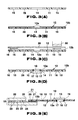
- the film substrate 11 made of polyimide, polyester, and so forth is prepared and then goes through the respective processings to form therein the device hole 14, openings 15, and a cutting groove 28, as shown in Fig. 3A.
- the device hole 14 is formed at the center of the film substrate 11 to a square profile, and on the right side of this device hole, the opening 15 for the convenience of folding is likewise formed widthwise of the film substrate 11 to a strip-like shape while on the left side of the device hole 14 there is also formed the cutting groove 28 with a slit-like profile.
- the cutting groove 28 provided in each IC module is for cutting off the substrate 11 and the wiring leads 12 which will be described later in detail, and the left side of the cutting groove, there is similarly formed an opening 15 of another IC module.
- a metal foil such as of copper, etc. is laminated with the process of etching to follow whereby to remove unnecessary portions from the foil, so that the wiring leads 12 of a given pattern will be generated.
- the inner ends 12a of the wiring leads 12 extend, projecting inward within the device hole 14 while the outer end sides of the wiring leads 12 bridge the opening 15 and the cutting groove 28, respectively, with the outer ends 12b arranged at the periphery of the film substrate 11. It is noted that the entire surfaces of the wiring leads 12 are provided with a solder plating.
- the opening 15 is filled with epoxy resin-based electrically insulative plastic 16 in a manner to coat the respective surfaces of the wiring leads, certain portions of which bridge each of the openings 15.
- a tape-like exfoliator strip 29 wound in advance in a roll is coated at its spot, which is to be correspond to the opening 15 of the film substrate 11, with the electrically insulative plastic 16 to a uniform thickness.
- the exfoliator strip 29 is pulled out upward of the film substrate 11 so that the electrically insulative plastic 16 applied at the above-mentioned spot on the exfoliator strip will face each opening 15 of the IC module.
- the electrically insulative plastic on the exfoliator strip is thermally pressed against the wiring leads 12 which bridge the opening 15 so that said insulative plastic 16 will be transferred over to the respective surfaces of the wiring leads 12, whereby the electrically insulative plastic 16 gets deposited on the respective surfaces of the wiring leads 12 bridging the opening 15, with an electrically insulative plastic coating thereby produced over the wiring lead surfaces, and the space within the opening 15 whereby filled up with the electrically insulative plastic 16.
- each electrically insulative plastic 16 is provided at said spot to a uniform thickness on the surface of the exfoliator strip 29, the coatings produced over the respective surfaces of the wiring leads exhibit a uniform thickness.
- the IC chip 13 is put into the device hole 14 from under the film substrate 11, and then, the bumps 17 of the IC chip 13 are thermally pressure-welded to the respective inner ends 12a of the wiring leads 12 projecting inward within the device hole 14, wherein said thermal pressure welding between the bumps of the IC chip and the respective inner ends of the wiring leads 12 is effected, utilizing the solder plating provided over the surfaces of the wiring leads 12.
- both the film substrate 11 and the wiring leads 12 are cut off at the portion where the cutting groove 28 lies, whereby the wiring leads 12 bridging the opening 15 get coated with the electrically insulative plastic 16, and the IC module 10 having the IC chip 13 coupled to the respective inner ends 12a of the wiring leads 12 is formed as shown in Fig. 2.
- the IC module 10 is turned upside down and leftwide right, whereby the outer ends 12b of the wiring leads 12 may be coupled to the connection terminal 20 of the liquid crystal display panel 19, wherein the electrically conductive bonding agent is applied first over the entire area of the connection terminal of the liquid crystal display panel, followed by a step of coupling the outer ends 12b of the wiring leads 12 to the respective connection terminals 20 with the electrically conductive bonding compound 21 held therebetween, whereby due to the electrically conductive bonding compound 21, the outer ends 12b of the wiring leads 12 are coupled to the corresponding connection terminals 20 of the liquid crystal display panel 19 facing their counterpart outer ends 12b with electric conductivity provided between each two of said outer ends 12b and said counterpart connection terminals and with no trouble of subjecting the neighboring connection terminals into an accidental conductive contact with each other.
- the film substrate 11 is folded at a part where the opening 15 is located.
- the wiring leads 12 bridging the opening 15 incur bending at this time, since those portions of the wiring leads 12 situated at a folding part are coated with the electrically conductive plastic 16, said those portions are assured of high mechanical strength. Therefore, folding said those portions of the wiring leads 12 does not entail trouble of subjecting the wiring leads 12 to breakage.
- the wiring leads 12 arranged in a greatly narrow inter-wire gap pattern undergo lengthwide deformations at the time they are folded, the adjacent ones of the wiring leads 12 are ensured freedom from an accidental contact with one another which may lead to shortcircuiting, due to the existence of the electrically insulative plastic 16.
- the IC module 10 is of such a configuration comprising a 1st film substrate 11a and a 2nd film substrate, between which the wiring leads 12 are arranged as if they bridge the 1st and 2nd film substrate.
Landscapes
- Engineering & Computer Science (AREA)
- Microelectronics & Electronic Packaging (AREA)
- Wire Bonding (AREA)
Applications Claiming Priority (2)
| Application Number | Priority Date | Filing Date | Title |
|---|---|---|---|
| JP14731090 | 1990-06-07 | ||
| JP147310/90 | 1990-06-07 |
Publications (2)
| Publication Number | Publication Date |
|---|---|
| EP0460668A2 true EP0460668A2 (fr) | 1991-12-11 |
| EP0460668A3 EP0460668A3 (en) | 1992-05-27 |
Family
ID=15427305
Family Applications (1)
| Application Number | Title | Priority Date | Filing Date |
|---|---|---|---|
| EP19910109287 Withdrawn EP0460668A3 (en) | 1990-06-07 | 1991-06-06 | Ic module and a junction structure thereof |
Country Status (3)
| Country | Link |
|---|---|
| US (1) | US5161009A (fr) |
| EP (1) | EP0460668A3 (fr) |
| KR (1) | KR940006185Y1 (fr) |
Cited By (6)
| Publication number | Priority date | Publication date | Assignee | Title |
|---|---|---|---|---|
| FR2693341A1 (fr) * | 1992-07-03 | 1994-01-07 | Jaeger | Procédé de réalisation d'un ensemble électrique à circuit imprimé, notamment montre pour véhicules automobiles et produit obtenu. |
| EP0779772A4 (fr) * | 1994-09-27 | 1998-07-29 | Seiko Epson Corp | Carte a circuit imprime, son procede de production et dispositifs electroniques |
| EP1092676A4 (fr) * | 1999-03-31 | 2002-06-05 | Seiko Epson Corp | Connecteur a ecartement etroit, convertisseur d'ecartement, micromachine, actionneur piezo-electrique, actionneur electrostatique, tete d'impression a jet d'encre, imprimante a jet d'encre, dispositif a cristaux liquides et appareil electronique |
| EP1094029A4 (fr) * | 1999-03-31 | 2002-06-05 | Seiko Epson Corp | Connecteur a ecartement etroit, convertisseur d'ecartement, micromachine, actionneur piezo-electrique, actionneur electrostatique, tete d'impression a jet d'encre, imprimante a jet d'encre, dispositif a cristaux liquides et appareil electronique |
| US6885107B2 (en) | 2002-08-29 | 2005-04-26 | Micron Technology, Inc. | Flip-chip image sensor packages and methods of fabrication |
| CN100354730C (zh) * | 2001-02-28 | 2007-12-12 | 精工爱普生株式会社 | 柔性基板、电光装置和电子装置 |
Families Citing this family (27)
| Publication number | Priority date | Publication date | Assignee | Title |
|---|---|---|---|---|
| JP2821262B2 (ja) * | 1990-11-26 | 1998-11-05 | 株式会社日立製作所 | 電子装置 |
| JPH04301817A (ja) * | 1991-03-29 | 1992-10-26 | Rohm Co Ltd | 液晶表示装置とその製造方法 |
| JP3610077B2 (ja) * | 1992-03-26 | 2005-01-12 | セイコーエプソン株式会社 | 液晶表示装置および電子機器 |
| DE69331873T2 (de) * | 1992-12-26 | 2002-11-14 | Canon K.K., Tokio/Tokyo | Flüssigkristallapparat |
| JPH06334279A (ja) * | 1993-05-20 | 1994-12-02 | Minolta Camera Co Ltd | 多層フレキシブル電装基板 |
| JP2878066B2 (ja) | 1993-05-24 | 1999-04-05 | シャープ株式会社 | 印刷回路基板の接続方法 |
| US5436744A (en) * | 1993-09-03 | 1995-07-25 | Motorola Inc. | Flexible liquid crystal display with integrated driver circuit and display electrodes formed on opposite sides of folded substrate |
| JP3186925B2 (ja) * | 1994-08-04 | 2001-07-11 | シャープ株式会社 | パネルの実装構造並びに集積回路搭載テープおよびその製造方法 |
| JP2586344B2 (ja) * | 1994-09-30 | 1997-02-26 | 日本電気株式会社 | キャリアフィルム |
| JP3098392B2 (ja) * | 1995-03-03 | 2000-10-16 | シャープ株式会社 | 実装基板及びそれを用いた液晶モジュール |
| GB2307598B (en) * | 1995-11-24 | 2000-02-23 | Varintelligent | Combined printed circuit board and integrated circuit driver |
| US6738123B1 (en) * | 1996-03-15 | 2004-05-18 | Canon Kabushiki Kaisha | Drive circuit connection structure including a substrate, circuit board, and semiconductor device, and display apparatus including the connection structure |
| JP3695893B2 (ja) * | 1996-12-03 | 2005-09-14 | 沖電気工業株式会社 | 半導体装置とその製造方法および実装方法 |
| JPH10186393A (ja) * | 1996-12-19 | 1998-07-14 | Shin Etsu Polymer Co Ltd | 液晶表示パネルの表示検査用コネクタ及びその製造方法 |
| US6040624A (en) * | 1997-10-02 | 2000-03-21 | Motorola, Inc. | Semiconductor device package and method |
| US5956234A (en) * | 1998-01-20 | 1999-09-21 | Integrated Device Technology, Inc. | Method and structure for a surface mountable rigid-flex printed circuit board |
| CN100365808C (zh) * | 1999-03-31 | 2008-01-30 | 精工爱普生株式会社 | 窄间距用连接器、静电传动器、压电传动器和喷墨头 |
| US6823133B1 (en) * | 1999-11-15 | 2004-11-23 | Lexmark International, Inc. | Apparatus and method for electronic control of DC motor using an all-digital phase-locked loop |
| KR100921454B1 (ko) * | 2002-11-29 | 2009-10-13 | 엘지전자 주식회사 | 가전제품용 lcd 어셈블리의 인쇄회로기판 구조 |
| JP2004266236A (ja) * | 2003-01-09 | 2004-09-24 | Sony Chem Corp | 基板素片とその基板素片を用いた複合配線板 |
| US6966800B2 (en) * | 2004-03-22 | 2005-11-22 | Fci Americas Technology, Inc. | Overmolded electrical connector |
| WO2009055069A2 (fr) * | 2007-10-25 | 2009-04-30 | Chipstack Inc. | Module boîtier multiple utilisant une carte à circuit imprimé flex-rigide |
| CN102026475B (zh) * | 2009-09-22 | 2012-03-21 | 群康科技(深圳)有限公司 | 软性印刷电路板及显示器制造方法 |
| US8018229B1 (en) | 2010-04-22 | 2011-09-13 | Honeywell International Inc. | Structure and method for flex circuit on a chip |
| KR102148845B1 (ko) * | 2013-12-12 | 2020-08-27 | 엘지이노텍 주식회사 | 인쇄회로기판 |
| US10163687B2 (en) * | 2015-05-22 | 2018-12-25 | Qualcomm Incorporated | System, apparatus, and method for embedding a 3D component with an interconnect structure |
| US11889728B2 (en) | 2018-08-28 | 2024-01-30 | Sharp Kabushiki Kaisha | Display device |
Family Cites Families (5)
| Publication number | Priority date | Publication date | Assignee | Title |
|---|---|---|---|---|
| US4514042A (en) * | 1981-09-30 | 1985-04-30 | Sharp Kabushiki Kaisha | Thin structure of display panel |
| US4631820A (en) * | 1984-08-23 | 1986-12-30 | Canon Kabushiki Kaisha | Mounting assembly and mounting method for an electronic component |
| JPS6246482U (fr) * | 1985-09-06 | 1987-03-20 | ||
| JP2641869B2 (ja) * | 1987-07-24 | 1997-08-20 | 三菱電機株式会社 | 半導体装置の製造方法 |
| JPH03125444A (ja) * | 1989-10-09 | 1991-05-28 | Chisso Corp | 改良されたフィルムキャリヤー |
-
1991
- 1991-05-22 KR KR2019910007285U patent/KR940006185Y1/ko not_active Expired - Lifetime
- 1991-05-31 US US07/708,346 patent/US5161009A/en not_active Expired - Fee Related
- 1991-06-06 EP EP19910109287 patent/EP0460668A3/en not_active Withdrawn
Cited By (15)
| Publication number | Priority date | Publication date | Assignee | Title |
|---|---|---|---|---|
| FR2693341A1 (fr) * | 1992-07-03 | 1994-01-07 | Jaeger | Procédé de réalisation d'un ensemble électrique à circuit imprimé, notamment montre pour véhicules automobiles et produit obtenu. |
| EP0779772A4 (fr) * | 1994-09-27 | 1998-07-29 | Seiko Epson Corp | Carte a circuit imprime, son procede de production et dispositifs electroniques |
| EP1092676A4 (fr) * | 1999-03-31 | 2002-06-05 | Seiko Epson Corp | Connecteur a ecartement etroit, convertisseur d'ecartement, micromachine, actionneur piezo-electrique, actionneur electrostatique, tete d'impression a jet d'encre, imprimante a jet d'encre, dispositif a cristaux liquides et appareil electronique |
| EP1094029A4 (fr) * | 1999-03-31 | 2002-06-05 | Seiko Epson Corp | Connecteur a ecartement etroit, convertisseur d'ecartement, micromachine, actionneur piezo-electrique, actionneur electrostatique, tete d'impression a jet d'encre, imprimante a jet d'encre, dispositif a cristaux liquides et appareil electronique |
| US6577370B1 (en) | 1999-03-31 | 2003-06-10 | Seiko Epson Corporation | Narrow-pitch connector, pitch converter, micromachine, piezoelectric actuator, electrostatic actuator, ink-jet head, ink-jet printer, liquid crystal device, and electronic apparatus |
| US6601947B1 (en) | 1999-03-31 | 2003-08-05 | Seiko Epson Corporation | Narrow-pitch connector, electrostatic actuator, piezoelectric actuator, ink-jet head, ink-jet printer, micromachine, liquid crystal panel, and electronic apparatus |
| CN100354730C (zh) * | 2001-02-28 | 2007-12-12 | 精工爱普生株式会社 | 柔性基板、电光装置和电子装置 |
| US6885107B2 (en) | 2002-08-29 | 2005-04-26 | Micron Technology, Inc. | Flip-chip image sensor packages and methods of fabrication |
| US6956295B2 (en) | 2002-08-29 | 2005-10-18 | Micron Technology, Inc. | Flip-chip image sensor packages |
| US6964886B2 (en) * | 2002-08-29 | 2005-11-15 | Micron Technology, Inc. | Methods of fabrication for flip-chip image sensor packages |
| US7122390B2 (en) | 2002-08-29 | 2006-10-17 | Micron Technology, Inc. | Methods of fabrication for flip-chip image sensor packages |
| US6940141B2 (en) | 2002-08-29 | 2005-09-06 | Micron Technology, Inc. | Flip-chip image sensor packages and methods of fabrication |
| US7443038B2 (en) | 2002-08-29 | 2008-10-28 | Micron Technology, Inc. | Flip-chip image sensor packages |
| US7638813B2 (en) | 2002-08-29 | 2009-12-29 | Micron Technology, Inc. | Methods of fabrication for flip-chip image sensor packages |
| US8097895B2 (en) | 2002-08-29 | 2012-01-17 | Round Rock Research, Llc | Electronic device package with an optical device |
Also Published As
| Publication number | Publication date |
|---|---|
| US5161009A (en) | 1992-11-03 |
| KR940006185Y1 (ko) | 1994-09-10 |
| EP0460668A3 (en) | 1992-05-27 |
| KR920001477U (ko) | 1992-01-28 |
Similar Documents
| Publication | Publication Date | Title |
|---|---|---|
| US5161009A (en) | Ic module having a folding junction structure | |
| EP0459493B1 (fr) | Dispositif semi-conducteur comprenant une bande pour connexion automatique TAB et son procédé de fabrication | |
| US4999460A (en) | Conductive connecting structure | |
| US5820014A (en) | Solder preforms | |
| US4727633A (en) | Method of securing metallic members together | |
| US4949158A (en) | Semiconductor device | |
| US5180888A (en) | Conductive bonding agent and a conductive connecting method | |
| JP3482850B2 (ja) | 半導体装置及びその製造方法、回路基板並びに電子機器 | |
| US4064356A (en) | Soldered joint | |
| US7459771B2 (en) | Assembly structure for electronic power integrated circuit formed on a semiconductor die and corresponding manufacturing process | |
| EP0413161B1 (fr) | Structure de connexion conductrice | |
| JPH0371570A (ja) | 導電用結合剤および導電接続構造 | |
| JP3096226B2 (ja) | 半導体装置の製造方法 | |
| JP3080106B2 (ja) | Icモジュールの接続方法 | |
| JPS6326545B2 (fr) | ||
| JPH0878599A (ja) | 集積回路パッケージ及びその製造方法 | |
| JP2816084B2 (ja) | 半田塗布方法、半導体装置の製造方法およびスキージ | |
| KR890000596Y1 (ko) | 배선기판 | |
| JPS61214548A (ja) | テ−プキヤリア | |
| JP2954559B2 (ja) | 配線基板の電極構造 | |
| JP3356341B2 (ja) | Tabテープ及びその製造方法並びに半導体装置 | |
| JP3149083B2 (ja) | 導電用結合剤および導電接続構造 | |
| JPH05160559A (ja) | プリント配線板 | |
| JPH02296345A (ja) | 半導体装置 | |
| JPH02252251A (ja) | フィルムキャリヤーテープ |
Legal Events
| Date | Code | Title | Description |
|---|---|---|---|
| PUAI | Public reference made under article 153(3) epc to a published international application that has entered the european phase |
Free format text: ORIGINAL CODE: 0009012 |
|
| 17P | Request for examination filed |
Effective date: 19910606 |
|
| AK | Designated contracting states |
Kind code of ref document: A2 Designated state(s): DE FR GB |
|
| PUAL | Search report despatched |
Free format text: ORIGINAL CODE: 0009013 |
|
| AK | Designated contracting states |
Kind code of ref document: A3 Designated state(s): DE FR GB |
|
| STAA | Information on the status of an ep patent application or granted ep patent |
Free format text: STATUS: THE APPLICATION HAS BEEN WITHDRAWN |
|
| 18W | Application withdrawn |
Withdrawal date: 19920819 |