EP0461896A2 - Système de traitement de signal numérique - Google Patents
Système de traitement de signal numérique Download PDFInfo
- Publication number
- EP0461896A2 EP0461896A2 EP91305350A EP91305350A EP0461896A2 EP 0461896 A2 EP0461896 A2 EP 0461896A2 EP 91305350 A EP91305350 A EP 91305350A EP 91305350 A EP91305350 A EP 91305350A EP 0461896 A2 EP0461896 A2 EP 0461896A2
- Authority
- EP
- European Patent Office
- Prior art keywords
- signal
- analogue
- digital converter
- processor unit
- processing system
- Prior art date
- Legal status (The legal status is an assumption and is not a legal conclusion. Google has not performed a legal analysis and makes no representation as to the accuracy of the status listed.)
- Granted
Links
Images

Classifications
-
- H—ELECTRICITY
- H04—ELECTRIC COMMUNICATION TECHNIQUE
- H04N—PICTORIAL COMMUNICATION, e.g. TELEVISION
- H04N9/00—Details of colour television systems
- H04N9/64—Circuits for processing colour signals
Definitions
- This invention concerns a digital signal processing system of the kind wherein an incoming analogue signal is sampled at a rate determined by a frequency component of the analogue signal and converted to a series of digital words.
- a processing system is used, for example, in converting a composite colour television signal into the corresponding digital signal required for use in digital television systems.
- the sampling frequency In the operation of such a digital signal processing system, it is necessary that the sampling frequency have a fixed phase relationship to the incoming signal in order that information represented by the phase of a component of the signal can be correctly decoded. It is also important that any phase error that should occur between the incoming signal and the sampling frequency, for example upon change of a signal source, should be corrected as rapidly as possible.
- a first aspect of the invention provides a digital signal processing system comprising an analogue to digital converter arranged to receive an incoming analogue signal to be digitised and to provide digital output signals representing the amplitude of the incoming analogue signal sampled at a frequency corresponding to a multiple of the frequency of a signal component of the incoming signal, and a processor unit programmed to receive said output signals, to store and compare one or more sets of said amplitude signals corresponding to one or more cycles of the said signal component, and to derive from said comparison a value representing a phase error between the sampling frequency of the analogue to digital converter and the said signal component.
- said processor unit is further programmed to determine, by comparison of a set of sampled amplitude signals corresponding to one cycle of said signal component, that sample closest to a given zero crossing point of said cycle of said signal component, and to compute said phase error value by comparison of the amplitude of said sample with a notional value of a sample coinciding with said crossing point.
- a second aspect of the invention provides a digital signal processing system comprising an analogue to digital converter arranged to receive an incoming analogue signal that is to be digitised, a variable frequency clock oscillator for controlling a sampling frequency at which said analogue to digital converter is to be operated, a phase shifter coupled between said clock oscillator and said analogue to digital converter and a processor unit arranged to receive sampled digital signal values provided by said analogue to digital converter and to provide output control signals to said variable frequency oscillator and to said phase shifter, said processor unit being programmed to compute from sampled signal values provided thereto a phase error between the said sampling frequency and a signal component of the incoming analogue signal, to provide a corresponding control signal to said phase shifter when the phase error is greater than a predetermined magnitude and to provide a corresponding control signal to said variable frequency oscillator when the phase error is below said predetermined magnitude.
- the sampling frequency of the analogue to digital converter is preferably four times the frequency of the colour subcarrier of the composite video waveform, and the signal component of the incoming analogue signal with reference to which the phase error is computed is the colour burst of the composite video waveform.
- the said phase shifter comprises a tapped delay line and the control signal provided to the phase shifter from the processor unit controls the selection of that tap of the delay line from which the oscillator signal is supplied to the analogue to digital converter.
- the processor unit is programmed to receive and store sampled signal values received during each cycle of a colour burst, in such a manner that the respective values corresponding to a single cycle of the colour burst are averaged over a plurality of cycles before the phase error is computed. This enables correction to be achieved for burst envelope distortion and noise.
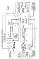
- a signal processing system in accordance with one embodiment of the invention is adapted for the analogue to digital conversion of a composite colour video signal received at a signal input 1.
- An analogue conditioning circuit indicated generally at 2 is arranged to set the signal voltage limits to defined levels and to extract timing information from the conventional video synchronising pulses of the composite video signal. This timing information is provided from an output indicated at 3, whereas the conditioned composite video signal is applied from an output 4 to an input of an analogue to digital converter 5.
- the analogue to digital converter 5 is clocked to sample the composite video signal at a repetition frequency corresponding to four times the frequency of the colour subcarrier of the composite video waveform, by means of clock pulses derived from a voltage controlled oscillator 6 and applied to the analogue to digital converter via a phase shifter 7, a flywheel circuit 8 and a divider circuit 9. At each clock pulse applied to the analogue to digital converter 5 the latter provides at an output 10 a corresponding digital word corresponding to the voltage amplitude of the incoming analogue signal.
- the incoming analogue signal is sampled at four times the frequency of the colour subcarrier, when the phase of the clock pulses supplied to the analogue to digital converter 5 are correctly locked to the phase of the colour subcarrier of the incoming signal the voltage amplitudes of the four samples obtained during each cycle of the subcarrier represent four different relationships of sample sign or phase from which the colour information carried by the original can be decoded.
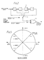
- Figure 5 illustrates the appropriate phase relationship between the colour subcarrier and the four samples required to be obtained during each cycle, and the locking of the sampling axes to the phase of the colour subcarrier is achieved by adjusting the frequency of the clock oscillator 6 and the phase shift provided by the phase shifter 7 with the aid of a programmed microprocessor control system as indicated within the box 11 shown in broken lines in Fig. 1.
- the system comprises a main processor unit 12 and a tag word counter 13, both of which receive the same clock pulses as the analogue to digital converter 5 and thus operate at a system frequency corresponding to the sampling frequency of the analogue to digital converter.
- the processor 12 is associated with read only memory 13 containing the control program and random access memory 14 for storing the results of processing operations.
- the processor 12 incorporates a data selector indicated diagrammatically at 15, which, when enabled by an appropriate signal from an output 16 of the processor 12, causes the processor 12 to read selectively digital words from the output 10 of the analogue to digital converter 5 and to read associated tag words from the tag word counter 13.
- the processor 12 further comprises an input 17 for receiving video synchronising signals from the output 3 of the conditioner 2, a data output 18 to control ports 19 of the processing system and control outputs 20 and 21 for the phase shifter 7 and variable frequency oscillator 6 respectively.
- the processing system 11 is programmed to compute, from the digital signals received at 10, the synchronising signals received at 17 and the clock pulse signals received from the divider 9 a phase error between the clock pulse signals and the colour subcarrier of the incoming analogue composite video signal and to provide a corresponding error signal on one of the two outputs 20 and 21 in accordance with whether the magnitude of the error is greater or less than a predetermined value. Fast locking of the phase of the clock pulse signals to that of the composite video signal can thus be obtained in a manner that will now be described.
- the variable frequency oscillator 6 comprises a stable voltage controlled oscillator which runs at eight times the nominal subcarrier frequency and generates the system clocks for feeding into the phase shifter 7.
- the oscillator 6 can be steered in frequency under control of the processor 12 via a digital to analogue converter 22. However changes in phase will take place over large numbers of cycles because of the limited pulling range of the oscillator and hence the primary fast control of phase lock is achieved with the phase shifter 7, which is adapted to provide fast switching of increments of phase shift via a selector 23 controlled from the output 20 of processor 12.
- the oscillator 6 is slowly pulled onto frequency with a second order loop filter implemented in the processor instructions as described below.
- the phase shifter 7 comprises a tapped delay line 71 and a programmable selector 72.
- Each tap off the delay line 71 is equivalent to the required resolution of phase step at subcarrier frequency, and is applied to individual inputs of the selector 72. Since the input frequency into the delay line 71 is eight times subcarrier, the delay taps move by a total of one eighth of a cycle of subcarrier frequency for a complete cycle of 360 degrees, in steps of approximately one nano-second.
- a programmable inverter 73 can be placed after the selected output and the total delay reduced to 180 degrees or half a cycle of the oscillator frequency.
- the processor 12 applies a continuous series of steps to the programmable selector in response to a measured colour burst phase error, which has the effect of sliding the selector output along the delay line and consequently shifting the output phase.
- Each 360 degree movement of the oscillator phase is equivalent to 180 degrees at the system clock frequency.
- the system will provide the necessary rotation of a full 360 degrees at four times subcarrier by sliding the selector along the delay line up to twice per line time. An error can therefore be corrected extremely quickly using the phase shifter 7.
- the clock flywheel circuit 8 removes any spikes or glitches produced on the clock by the action of the processor in moving the phase shifter.
- the clean clocks are then divided by two in the divider 9 to produce a clean, even mark/space ratio system clock at four times nominal subcarrier frequency.
- Fig. 5 is a vector diagram showing the correct, in-phase relationship between the sampling axes as defined by the system clock pulses, and the axes of the conventional chrominance signal components of the colour subcarrier of the composite video signal.
- the upper part of Fig. 4 shows the corresponding in-phase relationship between the waveform of the conventional colour burst signal of the composite waveform indicated at 100, and the digital values, indicated at 102, obtained by sampling the colour burst of the composite video signal, when the system clock pulses are correctly phase locked with no phase error.
- phase error 4 shows, for comparison, the corresponding relationship when a phase error of less than 45° occurs between the colour burst waveform and the clock pulses.
- the phase error can be determined from the corresponding amplitude error that will occur in the digital value of that sample which is closest to a zero crossing point of the colour burst waveform.
- the phase error will thus be the arc-sine of the amplitude error represented by the difference between the sampled digital value and the digital value that would correspond to a zero crossing point of the waveform.
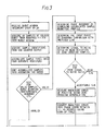
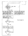
- Fig. 3 is a flow chart illustrating the programming of the processor system 11 required to affect the above-mentioned computation and provide a corresponding control signal to the oscillator 6 or phase shifter 7 of Fig. 1.
- the individual steps of the flow chart will be understood by one skilled in the art without further detailed explanation, and therefore the relationship between the flow chart and the foregoing description will be summarised only briefly.
- the program commences with the wait for 'burst window', the presence of a burst window within which the colour burst of the composite video signal will occur being determined from the conventional synchronising signals received at input 17 of the processor 12.
- the sampled digital values from the analogue to digital converter 5 are received via a digital subcarrier band-pass filter, not shown in Fig. 1, and the data selector 15 and stored in the random access memory 14 to provide, for each of the ten cycles of the colour burst, four sampled digital values corresponding to the samples 102 of Fig. 4.
- the processor 12 then also receives from the tag word counter 13 corresponding tag words that are associated with each of the sampled and stored digital values, so that corresponding samples from each of the cycles of the colour burst signal are each identified by the same tag word to identify the relative positions of the samples within the cycle.
- This relationship between samples and tag words is illustrated in Fig. 4.
- Each set of samples identified by the same tag word is then accumulated in an individual register to provide an integrated value for the entire period of the colour burst signal. This averaging will provide immunity to burst envelope distortion and noise.
- the four accumulated samples are then processed to determine the phase error from the amplitude error of that sample identified as being closest to the positive going zero crossing point of the colour burst waveform. Selection of the appropriate sample type will ensure that the phase error is within plus or minus 45° and a corresponding adjustment of the phase shifter 7 or the oscillator 6 can then be initiated in accordance with the determined magnitude of the phase error.
- the above described measurement and correction loop enables the system to acquire the phase, and where appropriate the PAL ident, of the incoming colour burst within three line times and provides extremely quick recovery from non-synchronous changes in the incoming signal to bring the clocks back into a known phase.
- the use of digital techniques in the system also conveys other advantages to enhance performance over conventional analogue locking methods, by directly measuring the amount of noise present during the colour burst, and indicating the colour burst amplitude. These measurements may then be used to modify characteristics within the system such as alteration of loop filtering for noisy signals, and automatic corrections for low amplitude incoming subcarrier by simple condition testing in the processor program. All the functions provided by a conventional analogue phase locked oscillator, such as the loop filtering and PAL ident extraction are implemented in the program and are therefore capable of being dynamically altered by the processor to optimise locking conditions.
Landscapes
- Engineering & Computer Science (AREA)
- Multimedia (AREA)
- Signal Processing (AREA)
- Processing Of Color Television Signals (AREA)
Applications Claiming Priority (2)
| Application Number | Priority Date | Filing Date | Title |
|---|---|---|---|
| GB909013151A GB9013151D0 (en) | 1990-06-13 | 1990-06-13 | Digital signal processing system |
| GB9013151 | 1990-06-13 |
Publications (3)
| Publication Number | Publication Date |
|---|---|
| EP0461896A2 true EP0461896A2 (fr) | 1991-12-18 |
| EP0461896A3 EP0461896A3 (en) | 1993-06-09 |
| EP0461896B1 EP0461896B1 (fr) | 1997-11-12 |
Family
ID=10677525
Family Applications (1)
| Application Number | Title | Priority Date | Filing Date |
|---|---|---|---|
| EP91305350A Expired - Lifetime EP0461896B1 (fr) | 1990-06-13 | 1991-06-13 | Système de traitement de signal numérique |
Country Status (3)
| Country | Link |
|---|---|
| EP (1) | EP0461896B1 (fr) |
| DE (1) | DE69128168T2 (fr) |
| GB (1) | GB9013151D0 (fr) |
Cited By (7)
| Publication number | Priority date | Publication date | Assignee | Title |
|---|---|---|---|---|
| EP0565333A3 (en) * | 1992-04-06 | 1994-05-11 | Questech Ltd | Apparatus for processing a pal colour television signal |
| EP0632664A3 (fr) * | 1993-07-01 | 1995-01-18 | Sony Corporation | Circuit de traitement d'un signal de chrominance |
| WO1996042171A1 (fr) * | 1995-06-09 | 1996-12-27 | Samsung Electronics Co., Ltd. | Equipement et procede de production d'un signal de synchronisation d'un segment de donnees |
| WO1996042170A1 (fr) * | 1995-06-09 | 1996-12-27 | Samsung Electronics Co., Ltd. | Circuit et procede de recuperation de rythme de symboles |
| EP0777391A3 (fr) * | 1995-11-30 | 1997-09-24 | Sanyo Electric Co | Appareil comprenant un convertisseur analogique-numérique pour le traitement d'un signal de télévision |
| ES2127161A1 (es) * | 1996-06-05 | 1999-04-01 | Samsung Electronics Co Ltd | Aparato y procedimiento para la generacion de una señal de sincronismo de un segmento de datos. |
| ES2129012A1 (es) * | 1996-06-05 | 1999-05-16 | Samsung Electronics Co Ltd | Circuito y procedimiento para la recuperacion de temporizacion de simbolos. |
Family Cites Families (6)
| Publication number | Priority date | Publication date | Assignee | Title |
|---|---|---|---|---|
| JPS5715586A (en) * | 1980-07-02 | 1982-01-26 | Sony Corp | Code modulator for video signal |
| DE3136522A1 (de) * | 1981-09-15 | 1983-03-24 | Siemens AG, 1000 Berlin und 8000 München | Verfahren und anordnung zur digitalen regelung der phase des systemtaktes eines digitalen signalverarbeitungssystems |
| US4463371A (en) * | 1982-05-28 | 1984-07-31 | Rca Corporation | Clock generation apparatus for a digital television system |
| US4636836A (en) * | 1984-12-03 | 1987-01-13 | Rca Corporation | Phase locked loop system for providing a phase shifted output signal |
| US4797730A (en) * | 1987-04-10 | 1989-01-10 | Ampex Corporation | Method and apparatus for controlling the sampling phase of an analog color television signal |
| US4847678A (en) * | 1988-01-11 | 1989-07-11 | Eastman Kodak Company | Dual mode gen-lock system which automatically locks to color burst or to sync information |
-
1990
- 1990-06-13 GB GB909013151A patent/GB9013151D0/en active Pending
-
1991
- 1991-06-13 DE DE69128168T patent/DE69128168T2/de not_active Expired - Fee Related
- 1991-06-13 EP EP91305350A patent/EP0461896B1/fr not_active Expired - Lifetime
Cited By (15)
| Publication number | Priority date | Publication date | Assignee | Title |
|---|---|---|---|---|
| EP0565333A3 (en) * | 1992-04-06 | 1994-05-11 | Questech Ltd | Apparatus for processing a pal colour television signal |
| EP0632664A3 (fr) * | 1993-07-01 | 1995-01-18 | Sony Corporation | Circuit de traitement d'un signal de chrominance |
| US5532757A (en) * | 1993-07-01 | 1996-07-02 | Sony Corporation | APC and ACC processing using common circuitry |
| GB2304476A (en) * | 1995-06-09 | 1997-03-19 | Samsung Electronics Co Ltd | Symbol timing recovery circuit and method |
| WO1996042170A1 (fr) * | 1995-06-09 | 1996-12-27 | Samsung Electronics Co., Ltd. | Circuit et procede de recuperation de rythme de symboles |
| GB2303759A (en) * | 1995-06-09 | 1997-02-26 | Samsung Electronics Co Ltd | Apparatus and method for generating data segment |
| WO1996042171A1 (fr) * | 1995-06-09 | 1996-12-27 | Samsung Electronics Co., Ltd. | Equipement et procede de production d'un signal de synchronisation d'un segment de donnees |
| GB2304476B (en) * | 1995-06-09 | 1999-09-29 | Samsung Electronics Co Ltd | Symbol timing recovery circuit and method |
| GB2303759B (en) * | 1995-06-09 | 2000-01-12 | Samsung Electronics Co Ltd | Apparatus and method for generating data segment sync signal |
| CN1058122C (zh) * | 1995-06-09 | 2000-11-01 | 三星电子株式会社 | 符号定时恢复电路和方法 |
| CN1068749C (zh) * | 1995-06-09 | 2001-07-18 | 三星电子株式会社 | 用于产生数据段同步信号的装置和方法 |
| EP0777391A3 (fr) * | 1995-11-30 | 1997-09-24 | Sanyo Electric Co | Appareil comprenant un convertisseur analogique-numérique pour le traitement d'un signal de télévision |
| US6201578B1 (en) | 1995-11-30 | 2001-03-13 | Sanyo Electric Co., Ltd. | Apparatus with A/D converter for processing television signal |
| ES2127161A1 (es) * | 1996-06-05 | 1999-04-01 | Samsung Electronics Co Ltd | Aparato y procedimiento para la generacion de una señal de sincronismo de un segmento de datos. |
| ES2129012A1 (es) * | 1996-06-05 | 1999-05-16 | Samsung Electronics Co Ltd | Circuito y procedimiento para la recuperacion de temporizacion de simbolos. |
Also Published As
| Publication number | Publication date |
|---|---|
| EP0461896B1 (fr) | 1997-11-12 |
| GB9013151D0 (en) | 1990-08-01 |
| DE69128168T2 (de) | 1998-04-09 |
| EP0461896A3 (en) | 1993-06-09 |
| DE69128168D1 (de) | 1997-12-18 |
Similar Documents
| Publication | Publication Date | Title |
|---|---|---|
| KR900006472B1 (ko) | 샘플링 클록 재생회로 | |
| US5500874A (en) | Digital filtering, data rate conversion and modem design | |
| US4692931A (en) | Synchronization circuit capable of establishing synchronism even when a sampling rate is invariable | |
| US6909467B2 (en) | Broadcast text data sampling apparatus and broadcast text data sampling method | |
| US4312075A (en) | Timing-phase recovery circuit | |
| US4510521A (en) | Circuit for adjusting the amplitude of a color signal | |
| KR950035391A (ko) | 고품위 텔레비젼 수신기에 있어서 기호 레이트의 약수에서 최종 중간 주파수 반송파를 갖는 디지탈잔류 측파대(vsb) 검출기 | |
| JPH10200594A (ja) | ディジタル復調器におけるシンボルタイミング復元回路 | |
| US4751565A (en) | Microprocessor controlled digital genlock | |
| KR970005216B1 (ko) | 위상 검출기 | |
| EP0461896B1 (fr) | Système de traitement de signal numérique | |
| US5130802A (en) | Television receiving section having an a/d converter which simultaneously performs synchronous demodulation | |
| US4570126A (en) | FM Demodulator using interpolation to approximate zero crossings | |
| EP0478024B1 (fr) | Dispositif pour améliorer des transitions de signal | |
| US20050265487A1 (en) | Method of sampling data and a circuit for sampling data | |
| US4852124A (en) | Digital phase-locked loop clock extractor for bipolar signals | |
| US5999577A (en) | Clock reproducing circuit for packet FSK signal receiver | |
| KR100466553B1 (ko) | 지연 정정 회로 | |
| US4535295A (en) | Method and device for controlling the phase of timing signal | |
| US4538172A (en) | Analog to digital converting system for composite video signal | |
| US4165488A (en) | Derangement detector in a receiver of a system for data transmission by means of phase modulation of a carrier | |
| JPH04234278A (ja) | 信号分離器 | |
| JPH05249942A (ja) | コンピュータ出力映像の画像サンプリング装置 | |
| JPS62292079A (ja) | 自動波形等化器 | |
| JPH0693778B2 (ja) | カラーテレビジヨン信号受信機 |
Legal Events
| Date | Code | Title | Description |
|---|---|---|---|
| PUAI | Public reference made under article 153(3) epc to a published international application that has entered the european phase |
Free format text: ORIGINAL CODE: 0009012 |
|
| AK | Designated contracting states |
Kind code of ref document: A2 Designated state(s): DE FR GB IT |
|
| PUAL | Search report despatched |
Free format text: ORIGINAL CODE: 0009013 |
|
| AK | Designated contracting states |
Kind code of ref document: A3 Designated state(s): DE FR GB IT |
|
| 17P | Request for examination filed |
Effective date: 19931208 |
|
| 17Q | First examination report despatched |
Effective date: 19951010 |
|
| GRAG | Despatch of communication of intention to grant |
Free format text: ORIGINAL CODE: EPIDOS AGRA |
|
| GRAH | Despatch of communication of intention to grant a patent |
Free format text: ORIGINAL CODE: EPIDOS IGRA |
|
| GRAH | Despatch of communication of intention to grant a patent |
Free format text: ORIGINAL CODE: EPIDOS IGRA |
|
| GRAA | (expected) grant |
Free format text: ORIGINAL CODE: 0009210 |
|
| AK | Designated contracting states |
Kind code of ref document: B1 Designated state(s): DE FR GB IT |
|
| PG25 | Lapsed in a contracting state [announced via postgrant information from national office to epo] |
Ref country code: IT Free format text: LAPSE BECAUSE OF FAILURE TO SUBMIT A TRANSLATION OF THE DESCRIPTION OR TO PAY THE FEE WITHIN THE PRE;WARNING: LAPSES OF ITALIAN PATENTS WITH EFFECTIVE DATE BEFORE 2007 MAY HAVE OCCURRED AT ANY TIME BEFORE 2007. THE CORRECT EFFECTIVE DATE MAY BE DIFFERENT FROM THE ONE RECORDED.SCRIBED TIME-LIMIT Effective date: 19971112 |
|
| REF | Corresponds to: |
Ref document number: 69128168 Country of ref document: DE Date of ref document: 19971218 |
|
| ET | Fr: translation filed | ||
| PLBE | No opposition filed within time limit |
Free format text: ORIGINAL CODE: 0009261 |
|
| STAA | Information on the status of an ep patent application or granted ep patent |
Free format text: STATUS: NO OPPOSITION FILED WITHIN TIME LIMIT |
|
| 26N | No opposition filed | ||
| PGFP | Annual fee paid to national office [announced via postgrant information from national office to epo] |
Ref country code: GB Payment date: 20000614 Year of fee payment: 10 |
|
| PGFP | Annual fee paid to national office [announced via postgrant information from national office to epo] |
Ref country code: FR Payment date: 20000626 Year of fee payment: 10 |
|
| PGFP | Annual fee paid to national office [announced via postgrant information from national office to epo] |
Ref country code: DE Payment date: 20000629 Year of fee payment: 10 |
|
| PG25 | Lapsed in a contracting state [announced via postgrant information from national office to epo] |
Ref country code: GB Free format text: LAPSE BECAUSE OF NON-PAYMENT OF DUE FEES Effective date: 20010613 |
|
| GBPC | Gb: european patent ceased through non-payment of renewal fee |
Effective date: 20010613 |
|
| PG25 | Lapsed in a contracting state [announced via postgrant information from national office to epo] |
Ref country code: FR Free format text: LAPSE BECAUSE OF NON-PAYMENT OF DUE FEES Effective date: 20020228 |
|
| PG25 | Lapsed in a contracting state [announced via postgrant information from national office to epo] |
Ref country code: DE Free format text: LAPSE BECAUSE OF NON-PAYMENT OF DUE FEES Effective date: 20020403 |