EP0464614A2 - Licht- oder strahlungsempfindliche Zusammensetzung - Google Patents
Licht- oder strahlungsempfindliche Zusammensetzung Download PDFInfo
- Publication number
- EP0464614A2 EP0464614A2 EP91110509A EP91110509A EP0464614A2 EP 0464614 A2 EP0464614 A2 EP 0464614A2 EP 91110509 A EP91110509 A EP 91110509A EP 91110509 A EP91110509 A EP 91110509A EP 0464614 A2 EP0464614 A2 EP 0464614A2
- Authority
- EP
- European Patent Office
- Prior art keywords
- light
- resist
- sensitivity
- composition
- radiation
- Prior art date
- Legal status (The legal status is an assumption and is not a legal conclusion. Google has not performed a legal analysis and makes no representation as to the accuracy of the status listed.)
- Granted
Links
- 230000005855 radiation Effects 0.000 title claims abstract description 106
- 230000035945 sensitivity Effects 0.000 title claims abstract description 102
- 239000000203 mixture Substances 0.000 title claims abstract description 83
- 229920000642 polymer Polymers 0.000 claims abstract description 113
- 230000001235 sensitizing effect Effects 0.000 claims abstract description 77
- 238000000034 method Methods 0.000 claims abstract description 58
- 230000008569 process Effects 0.000 claims abstract description 29
- 239000004065 semiconductor Substances 0.000 claims abstract description 23
- 238000006116 polymerization reaction Methods 0.000 claims abstract description 9
- 239000003795 chemical substances by application Substances 0.000 claims description 80
- 229920005601 base polymer Polymers 0.000 claims description 46
- 239000000758 substrate Substances 0.000 claims description 43
- -1 polysiloxane Polymers 0.000 claims description 30
- 238000010894 electron beam technology Methods 0.000 claims description 28
- 125000002887 hydroxy group Chemical group [H]O* 0.000 claims description 28
- 239000002253 acid Substances 0.000 claims description 25
- 239000003513 alkali Substances 0.000 claims description 23
- 229920001296 polysiloxane Polymers 0.000 claims description 23
- 150000003839 salts Chemical class 0.000 claims description 14
- 238000009499 grossing Methods 0.000 claims description 13
- 230000001681 protective effect Effects 0.000 claims description 12
- 238000012643 polycondensation polymerization Methods 0.000 claims description 8
- 125000003545 alkoxy group Chemical group 0.000 claims description 7
- 239000000975 dye Substances 0.000 claims description 7
- 238000005530 etching Methods 0.000 claims description 7
- 125000001997 phenyl group Chemical group [H]C1=C([H])C([H])=C(*)C([H])=C1[H] 0.000 claims description 7
- 150000001450 anions Chemical class 0.000 claims description 6
- 238000006555 catalytic reaction Methods 0.000 claims description 5
- 238000010438 heat treatment Methods 0.000 claims description 5
- 125000000217 alkyl group Chemical group 0.000 claims description 4
- 150000001768 cations Chemical class 0.000 claims description 4
- 229950000688 phenothiazine Drugs 0.000 claims description 4
- 239000002798 polar solvent Substances 0.000 claims description 4
- 229920000734 polysilsesquioxane polymer Polymers 0.000 claims description 4
- 239000004215 Carbon black (E152) Substances 0.000 claims description 3
- 150000008365 aromatic ketones Chemical group 0.000 claims description 3
- 229930195733 hydrocarbon Natural products 0.000 claims description 3
- 150000002430 hydrocarbons Chemical class 0.000 claims description 3
- 125000000951 phenoxy group Chemical group [H]C1=C([H])C([H])=C(O*)C([H])=C1[H] 0.000 claims description 3
- BDHFUVZGWQCTTF-UHFFFAOYSA-M sulfonate Chemical compound [O-]S(=O)=O BDHFUVZGWQCTTF-UHFFFAOYSA-M 0.000 claims description 3
- 239000012954 diazonium Substances 0.000 claims description 2
- 150000001989 diazonium salts Chemical class 0.000 claims description 2
- 125000001484 phenothiazinyl group Chemical group C1(=CC=CC=2SC3=CC=CC=C3NC12)* 0.000 claims 1
- 239000010408 film Substances 0.000 description 89
- 239000000463 material Substances 0.000 description 85
- 239000000243 solution Substances 0.000 description 51
- WGTYBPLFGIVFAS-UHFFFAOYSA-M tetramethylammonium hydroxide Chemical compound [OH-].C[N+](C)(C)C WGTYBPLFGIVFAS-UHFFFAOYSA-M 0.000 description 50
- XUIMIQQOPSSXEZ-UHFFFAOYSA-N Silicon Chemical compound [Si] XUIMIQQOPSSXEZ-UHFFFAOYSA-N 0.000 description 35
- 229910052710 silicon Inorganic materials 0.000 description 35
- 239000010703 silicon Substances 0.000 description 35
- LRHPLDYGYMQRHN-UHFFFAOYSA-N N-Butanol Chemical compound CCCCO LRHPLDYGYMQRHN-UHFFFAOYSA-N 0.000 description 16
- 150000001875 compounds Chemical class 0.000 description 16
- 239000007864 aqueous solution Substances 0.000 description 15
- 230000007423 decrease Effects 0.000 description 15
- 238000004519 manufacturing process Methods 0.000 description 15
- LFQSCWFLJHTTHZ-UHFFFAOYSA-N Ethanol Chemical compound CCO LFQSCWFLJHTTHZ-UHFFFAOYSA-N 0.000 description 14
- 238000006243 chemical reaction Methods 0.000 description 14
- 238000011161 development Methods 0.000 description 14
- 238000010586 diagram Methods 0.000 description 13
- 238000001312 dry etching Methods 0.000 description 12
- VYPSYNLAJGMNEJ-UHFFFAOYSA-N Silicium dioxide Chemical compound O=[Si]=O VYPSYNLAJGMNEJ-UHFFFAOYSA-N 0.000 description 11
- 125000001301 ethoxy group Chemical group [H]C([H])([H])C([H])([H])O* 0.000 description 10
- 125000002496 methyl group Chemical group [H]C([H])([H])* 0.000 description 10
- 229920003217 poly(methylsilsesquioxane) Polymers 0.000 description 10
- 150000003254 radicals Chemical class 0.000 description 10
- 229930192627 Naphthoquinone Natural products 0.000 description 9
- 230000007062 hydrolysis Effects 0.000 description 9
- 238000006460 hydrolysis reaction Methods 0.000 description 9
- 239000003960 organic solvent Substances 0.000 description 9
- 229920001721 polyimide Polymers 0.000 description 9
- 238000002834 transmittance Methods 0.000 description 9
- 239000000126 substance Substances 0.000 description 8
- XLYOFNOQVPJJNP-UHFFFAOYSA-N water Substances O XLYOFNOQVPJJNP-UHFFFAOYSA-N 0.000 description 8
- 230000007812 deficiency Effects 0.000 description 7
- 235000019441 ethanol Nutrition 0.000 description 7
- 239000011347 resin Substances 0.000 description 7
- 229920005989 resin Polymers 0.000 description 7
- ZWEHNKRNPOVVGH-UHFFFAOYSA-N 2-Butanone Chemical compound CCC(C)=O ZWEHNKRNPOVVGH-UHFFFAOYSA-N 0.000 description 6
- KFZMGEQAYNKOFK-UHFFFAOYSA-N Isopropanol Chemical compound CC(C)O KFZMGEQAYNKOFK-UHFFFAOYSA-N 0.000 description 6
- 238000009826 distribution Methods 0.000 description 6
- 239000003999 initiator Substances 0.000 description 6
- 238000001459 lithography Methods 0.000 description 6
- 125000002080 perylenyl group Chemical group C1(=CC=C2C=CC=C3C4=CC=CC5=CC=CC(C1=C23)=C45)* 0.000 description 6
- CSHWQDPOILHKBI-UHFFFAOYSA-N peryrene Natural products C1=CC(C2=CC=CC=3C2=C2C=CC=3)=C3C2=CC=CC3=C1 CSHWQDPOILHKBI-UHFFFAOYSA-N 0.000 description 6
- 229920002120 photoresistant polymer Polymers 0.000 description 6
- VYZAMTAEIAYCRO-UHFFFAOYSA-N Chromium Chemical compound [Cr] VYZAMTAEIAYCRO-UHFFFAOYSA-N 0.000 description 5
- 239000004642 Polyimide Substances 0.000 description 5
- QVGXLLKOCUKJST-UHFFFAOYSA-N atomic oxygen Chemical compound [O] QVGXLLKOCUKJST-UHFFFAOYSA-N 0.000 description 5
- 238000009833 condensation Methods 0.000 description 5
- 230000005494 condensation Effects 0.000 description 5
- 239000012046 mixed solvent Substances 0.000 description 5
- 239000001301 oxygen Substances 0.000 description 5
- 229910052760 oxygen Inorganic materials 0.000 description 5
- 235000012239 silicon dioxide Nutrition 0.000 description 5
- 238000004528 spin coating Methods 0.000 description 5
- 238000002835 absorbance Methods 0.000 description 4
- 230000003247 decreasing effect Effects 0.000 description 4
- 125000000524 functional group Chemical group 0.000 description 4
- UHOVQNZJYSORNB-UHFFFAOYSA-N monobenzene Natural products C1=CC=CC=C1 UHOVQNZJYSORNB-UHFFFAOYSA-N 0.000 description 4
- 239000000377 silicon dioxide Substances 0.000 description 4
- 239000007858 starting material Substances 0.000 description 4
- 125000000999 tert-butyl group Chemical group [H]C([H])([H])C(*)(C([H])([H])[H])C([H])([H])[H] 0.000 description 4
- WJFKNYWRSNBZNX-UHFFFAOYSA-N 10H-phenothiazine Chemical compound C1=CC=C2NC3=CC=CC=C3SC2=C1 WJFKNYWRSNBZNX-UHFFFAOYSA-N 0.000 description 3
- ZAMOUSCENKQFHK-UHFFFAOYSA-N Chlorine atom Chemical compound [Cl] ZAMOUSCENKQFHK-UHFFFAOYSA-N 0.000 description 3
- 238000010521 absorption reaction Methods 0.000 description 3
- 125000003118 aryl group Chemical group 0.000 description 3
- 230000008901 benefit Effects 0.000 description 3
- 230000008859 change Effects 0.000 description 3
- 239000000460 chlorine Substances 0.000 description 3
- 229910052801 chlorine Inorganic materials 0.000 description 3
- 238000006482 condensation reaction Methods 0.000 description 3
- 238000007796 conventional method Methods 0.000 description 3
- 125000004435 hydrogen atom Chemical group [H]* 0.000 description 3
- 238000010884 ion-beam technique Methods 0.000 description 3
- 150000003377 silicon compounds Chemical class 0.000 description 3
- 230000008961 swelling Effects 0.000 description 3
- 238000012546 transfer Methods 0.000 description 3
- FAYMLNNRGCYLSR-UHFFFAOYSA-M triphenylsulfonium triflate Chemical compound [O-]S(=O)(=O)C(F)(F)F.C1=CC=CC=C1[S+](C=1C=CC=CC=1)C1=CC=CC=C1 FAYMLNNRGCYLSR-UHFFFAOYSA-M 0.000 description 3
- 230000004304 visual acuity Effects 0.000 description 3
- 238000005406 washing Methods 0.000 description 3
- MCVVDMSWCQUKEV-UHFFFAOYSA-N (2-nitrophenyl)methyl 4-methylbenzenesulfonate Chemical compound C1=CC(C)=CC=C1S(=O)(=O)OCC1=CC=CC=C1[N+]([O-])=O MCVVDMSWCQUKEV-UHFFFAOYSA-N 0.000 description 2
- AZQWKYJCGOJGHM-UHFFFAOYSA-N 1,4-benzoquinone Chemical compound O=C1C=CC(=O)C=C1 AZQWKYJCGOJGHM-UHFFFAOYSA-N 0.000 description 2
- VEXZGXHMUGYJMC-UHFFFAOYSA-N Hydrochloric acid Chemical compound Cl VEXZGXHMUGYJMC-UHFFFAOYSA-N 0.000 description 2
- BAPJBEWLBFYGME-UHFFFAOYSA-N Methyl acrylate Chemical compound COC(=O)C=C BAPJBEWLBFYGME-UHFFFAOYSA-N 0.000 description 2
- PPBRXRYQALVLMV-UHFFFAOYSA-N Styrene Chemical compound C=CC1=CC=CC=C1 PPBRXRYQALVLMV-UHFFFAOYSA-N 0.000 description 2
- 150000007513 acids Chemical class 0.000 description 2
- 150000001555 benzenes Chemical class 0.000 description 2
- 230000015572 biosynthetic process Effects 0.000 description 2
- 125000004432 carbon atom Chemical group C* 0.000 description 2
- JHIVVAPYMSGYDF-UHFFFAOYSA-N cyclohexanone Chemical compound O=C1CCCCC1 JHIVVAPYMSGYDF-UHFFFAOYSA-N 0.000 description 2
- 239000004205 dimethyl polysiloxane Substances 0.000 description 2
- LIKFHECYJZWXFJ-UHFFFAOYSA-N dimethyldichlorosilane Chemical compound C[Si](C)(Cl)Cl LIKFHECYJZWXFJ-UHFFFAOYSA-N 0.000 description 2
- 229960004592 isopropanol Drugs 0.000 description 2
- 230000007246 mechanism Effects 0.000 description 2
- 125000000956 methoxy group Chemical group [H]C([H])([H])O* 0.000 description 2
- 239000005055 methyl trichlorosilane Substances 0.000 description 2
- JLUFWMXJHAVVNN-UHFFFAOYSA-N methyltrichlorosilane Chemical compound C[Si](Cl)(Cl)Cl JLUFWMXJHAVVNN-UHFFFAOYSA-N 0.000 description 2
- 125000000449 nitro group Chemical group [O-][N+](*)=O 0.000 description 2
- 229920003986 novolac Polymers 0.000 description 2
- 229920000435 poly(dimethylsiloxane) Polymers 0.000 description 2
- 239000002861 polymer material Substances 0.000 description 2
- 238000010992 reflux Methods 0.000 description 2
- 125000003808 silyl group Chemical group [H][Si]([H])([H])[*] 0.000 description 2
- 239000002904 solvent Substances 0.000 description 2
- 238000006467 substitution reaction Methods 0.000 description 2
- CPUDPFPXCZDNGI-UHFFFAOYSA-N triethoxy(methyl)silane Chemical compound CCO[Si](C)(OCC)OCC CPUDPFPXCZDNGI-UHFFFAOYSA-N 0.000 description 2
- JCVQKRGIASEUKR-UHFFFAOYSA-N triethoxy(phenyl)silane Chemical compound CCO[Si](OCC)(OCC)C1=CC=CC=C1 JCVQKRGIASEUKR-UHFFFAOYSA-N 0.000 description 2
- DLDWUFCUUXXYTB-UHFFFAOYSA-N (2-oxo-1,2-diphenylethyl) 4-methylbenzenesulfonate Chemical compound C1=CC(C)=CC=C1S(=O)(=O)OC(C=1C=CC=CC=1)C(=O)C1=CC=CC=C1 DLDWUFCUUXXYTB-UHFFFAOYSA-N 0.000 description 1
- DXUMYHZTYVPBEZ-UHFFFAOYSA-N 2,4,6-tris(trichloromethyl)-1,3,5-triazine Chemical compound ClC(Cl)(Cl)C1=NC(C(Cl)(Cl)Cl)=NC(C(Cl)(Cl)Cl)=N1 DXUMYHZTYVPBEZ-UHFFFAOYSA-N 0.000 description 1
- QRHHZFRCJDAUNA-UHFFFAOYSA-N 2-(4-methoxyphenyl)-4,6-bis(trichloromethyl)-1,3,5-triazine Chemical compound C1=CC(OC)=CC=C1C1=NC(C(Cl)(Cl)Cl)=NC(C(Cl)(Cl)Cl)=N1 QRHHZFRCJDAUNA-UHFFFAOYSA-N 0.000 description 1
- PTTPXKJBFFKCEK-UHFFFAOYSA-N 2-Methyl-4-heptanone Chemical compound CC(C)CC(=O)CC(C)C PTTPXKJBFFKCEK-UHFFFAOYSA-N 0.000 description 1
- ZNQVEEAIQZEUHB-UHFFFAOYSA-N 2-ethoxyethanol Chemical compound CCOCCO ZNQVEEAIQZEUHB-UHFFFAOYSA-N 0.000 description 1
- VHUUQVKOLVNVRT-UHFFFAOYSA-N Ammonium hydroxide Chemical compound [NH4+].[OH-] VHUUQVKOLVNVRT-UHFFFAOYSA-N 0.000 description 1
- 229910017048 AsF6 Inorganic materials 0.000 description 1
- LSNNMFCWUKXFEE-UHFFFAOYSA-M Bisulfite Chemical compound OS([O-])=O LSNNMFCWUKXFEE-UHFFFAOYSA-M 0.000 description 1
- 239000007848 Bronsted acid Substances 0.000 description 1
- DKPFZGUDAPQIHT-UHFFFAOYSA-N Butyl acetate Natural products CCCCOC(C)=O DKPFZGUDAPQIHT-UHFFFAOYSA-N 0.000 description 1
- 239000002841 Lewis acid Substances 0.000 description 1
- VVQNEPGJFQJSBK-UHFFFAOYSA-N Methyl methacrylate Chemical compound COC(=O)C(C)=C VVQNEPGJFQJSBK-UHFFFAOYSA-N 0.000 description 1
- 229910052581 Si3N4 Inorganic materials 0.000 description 1
- STOLYTNTPGXYRW-UHFFFAOYSA-N [nitro(phenyl)methyl] 4-methylbenzenesulfonate Chemical compound C1=CC(C)=CC=C1S(=O)(=O)OC([N+]([O-])=O)C1=CC=CC=C1 STOLYTNTPGXYRW-UHFFFAOYSA-N 0.000 description 1
- FLCWLOFMVFESNI-UHFFFAOYSA-N acridine-9(10H)-thione Chemical compound C1=CC=C2C(=S)C3=CC=CC=C3NC2=C1 FLCWLOFMVFESNI-UHFFFAOYSA-N 0.000 description 1
- 230000002411 adverse Effects 0.000 description 1
- XYLMUPLGERFSHI-UHFFFAOYSA-N alpha-Methylstyrene Chemical compound CC(=C)C1=CC=CC=C1 XYLMUPLGERFSHI-UHFFFAOYSA-N 0.000 description 1
- 239000004411 aluminium Substances 0.000 description 1
- 229910052782 aluminium Inorganic materials 0.000 description 1
- XAGFODPZIPBFFR-UHFFFAOYSA-N aluminium Chemical compound [Al] XAGFODPZIPBFFR-UHFFFAOYSA-N 0.000 description 1
- 239000000908 ammonium hydroxide Substances 0.000 description 1
- 125000003710 aryl alkyl group Chemical group 0.000 description 1
- 125000004429 atom Chemical group 0.000 description 1
- RWCCWEUUXYIKHB-UHFFFAOYSA-N benzophenone Chemical compound C=1C=CC=CC=1C(=O)C1=CC=CC=C1 RWCCWEUUXYIKHB-UHFFFAOYSA-N 0.000 description 1
- 239000012965 benzophenone Substances 0.000 description 1
- 125000001797 benzyl group Chemical group [H]C1=C([H])C([H])=C(C([H])=C1[H])C([H])([H])* 0.000 description 1
- 125000000051 benzyloxy group Chemical group [H]C1=C([H])C([H])=C(C([H])=C1[H])C([H])([H])O* 0.000 description 1
- 230000001588 bifunctional effect Effects 0.000 description 1
- 229910052799 carbon Inorganic materials 0.000 description 1
- 150000001732 carboxylic acid derivatives Chemical class 0.000 description 1
- 229910001914 chlorine tetroxide Inorganic materials 0.000 description 1
- 238000010276 construction Methods 0.000 description 1
- 238000000354 decomposition reaction Methods 0.000 description 1
- 230000002950 deficient Effects 0.000 description 1
- 229920006237 degradable polymer Polymers 0.000 description 1
- 230000000593 degrading effect Effects 0.000 description 1
- 238000006297 dehydration reaction Methods 0.000 description 1
- 238000001514 detection method Methods 0.000 description 1
- 125000005520 diaryliodonium group Chemical group 0.000 description 1
- 238000010790 dilution Methods 0.000 description 1
- 239000012895 dilution Substances 0.000 description 1
- 239000012153 distilled water Substances 0.000 description 1
- 239000000428 dust Substances 0.000 description 1
- 238000000609 electron-beam lithography Methods 0.000 description 1
- 238000002474 experimental method Methods 0.000 description 1
- 230000009477 glass transition Effects 0.000 description 1
- PCHJSUWPFVWCPO-UHFFFAOYSA-N gold Chemical compound [Au] PCHJSUWPFVWCPO-UHFFFAOYSA-N 0.000 description 1
- 239000010931 gold Substances 0.000 description 1
- 229910052737 gold Inorganic materials 0.000 description 1
- FUZZWVXGSFPDMH-UHFFFAOYSA-N hexanoic acid Chemical compound CCCCCC(O)=O FUZZWVXGSFPDMH-UHFFFAOYSA-N 0.000 description 1
- 125000006289 hydroxybenzyl group Chemical group 0.000 description 1
- 238000009413 insulation Methods 0.000 description 1
- 238000003475 lamination Methods 0.000 description 1
- 150000007517 lewis acids Chemical class 0.000 description 1
- QSHDDOUJBYECFT-UHFFFAOYSA-N mercury Chemical compound [Hg] QSHDDOUJBYECFT-UHFFFAOYSA-N 0.000 description 1
- 229910052753 mercury Inorganic materials 0.000 description 1
- 229910052751 metal Inorganic materials 0.000 description 1
- 239000002184 metal Substances 0.000 description 1
- 230000004048 modification Effects 0.000 description 1
- 238000012986 modification Methods 0.000 description 1
- 125000004573 morpholin-4-yl group Chemical group N1(CCOCC1)* 0.000 description 1
- 125000000962 organic group Chemical group 0.000 description 1
- VLTRZXGMWDSKGL-UHFFFAOYSA-M perchlorate Chemical compound [O-]Cl(=O)(=O)=O VLTRZXGMWDSKGL-UHFFFAOYSA-M 0.000 description 1
- 239000005011 phenolic resin Substances 0.000 description 1
- 238000006303 photolysis reaction Methods 0.000 description 1
- 230000015843 photosynthesis, light reaction Effects 0.000 description 1
- 238000001020 plasma etching Methods 0.000 description 1
- 229920003229 poly(methyl methacrylate) Polymers 0.000 description 1
- 230000000379 polymerizing effect Effects 0.000 description 1
- 239000004926 polymethyl methacrylate Substances 0.000 description 1
- 239000010453 quartz Substances 0.000 description 1
- 230000009467 reduction Effects 0.000 description 1
- 230000035939 shock Effects 0.000 description 1
- HQVNEWCFYHHQES-UHFFFAOYSA-N silicon nitride Chemical compound N12[Si]34N5[Si]62N3[Si]51N64 HQVNEWCFYHHQES-UHFFFAOYSA-N 0.000 description 1
- FDNAPBUWERUEDA-UHFFFAOYSA-N silicon tetrachloride Chemical compound Cl[Si](Cl)(Cl)Cl FDNAPBUWERUEDA-UHFFFAOYSA-N 0.000 description 1
- 239000007787 solid Substances 0.000 description 1
- 239000011877 solvent mixture Substances 0.000 description 1
- 230000000087 stabilizing effect Effects 0.000 description 1
- XTXNWQHMMMPKKO-UHFFFAOYSA-N tert-butyl 2-phenylethenyl carbonate Chemical compound CC(C)(C)OC(=O)OC=CC1=CC=CC=C1 XTXNWQHMMMPKKO-UHFFFAOYSA-N 0.000 description 1
- HJUGFYREWKUQJT-UHFFFAOYSA-N tetrabromomethane Chemical compound BrC(Br)(Br)Br HJUGFYREWKUQJT-UHFFFAOYSA-N 0.000 description 1
- QEMXHQIAXOOASZ-UHFFFAOYSA-N tetramethylammonium Chemical compound C[N+](C)(C)C QEMXHQIAXOOASZ-UHFFFAOYSA-N 0.000 description 1
- 238000002411 thermogravimetry Methods 0.000 description 1
- 239000010409 thin film Substances 0.000 description 1
- YRHRIQCWCFGUEQ-UHFFFAOYSA-N thioxanthen-9-one Chemical compound C1=CC=C2C(=O)C3=CC=CC=C3SC2=C1 YRHRIQCWCFGUEQ-UHFFFAOYSA-N 0.000 description 1
- 125000004665 trialkylsilyl group Chemical group 0.000 description 1
- 125000005409 triarylsulfonium group Chemical group 0.000 description 1
- 125000003866 trichloromethyl group Chemical group ClC(Cl)(Cl)* 0.000 description 1
- 125000000026 trimethylsilyl group Chemical group [H]C([H])([H])[Si]([*])(C([H])([H])[H])C([H])([H])[H] 0.000 description 1
- 238000001039 wet etching Methods 0.000 description 1
Images


Classifications
-
- G—PHYSICS
- G03—PHOTOGRAPHY; CINEMATOGRAPHY; ANALOGOUS TECHNIQUES USING WAVES OTHER THAN OPTICAL WAVES; ELECTROGRAPHY; HOLOGRAPHY
- G03F—PHOTOMECHANICAL PRODUCTION OF TEXTURED OR PATTERNED SURFACES, e.g. FOR PRINTING, FOR PROCESSING OF SEMICONDUCTOR DEVICES; MATERIALS THEREFOR; ORIGINALS THEREFOR; APPARATUS SPECIALLY ADAPTED THEREFOR
- G03F7/00—Photomechanical, e.g. photolithographic, production of textured or patterned surfaces, e.g. printing surfaces; Materials therefor, e.g. comprising photoresists; Apparatus specially adapted therefor
- G03F7/004—Photosensitive materials
- G03F7/075—Silicon-containing compounds
- G03F7/0757—Macromolecular compounds containing Si-O, Si-C or Si-N bonds
- G03F7/0758—Macromolecular compounds containing Si-O, Si-C or Si-N bonds with silicon- containing groups in the side chains
-
- Y—GENERAL TAGGING OF NEW TECHNOLOGICAL DEVELOPMENTS; GENERAL TAGGING OF CROSS-SECTIONAL TECHNOLOGIES SPANNING OVER SEVERAL SECTIONS OF THE IPC; TECHNICAL SUBJECTS COVERED BY FORMER USPC CROSS-REFERENCE ART COLLECTIONS [XRACs] AND DIGESTS
- Y10—TECHNICAL SUBJECTS COVERED BY FORMER USPC
- Y10S—TECHNICAL SUBJECTS COVERED BY FORMER USPC CROSS-REFERENCE ART COLLECTIONS [XRACs] AND DIGESTS
- Y10S430/00—Radiation imagery chemistry: process, composition, or product thereof
- Y10S430/1053—Imaging affecting physical property or radiation sensitive material, or producing nonplanar or printing surface - process, composition, or product: radiation sensitive composition or product or process of making binder containing
- Y10S430/1055—Radiation sensitive composition or product or process of making
- Y10S430/114—Initiator containing
- Y10S430/117—Free radical
-
- Y—GENERAL TAGGING OF NEW TECHNOLOGICAL DEVELOPMENTS; GENERAL TAGGING OF CROSS-SECTIONAL TECHNOLOGIES SPANNING OVER SEVERAL SECTIONS OF THE IPC; TECHNICAL SUBJECTS COVERED BY FORMER USPC CROSS-REFERENCE ART COLLECTIONS [XRACs] AND DIGESTS
- Y10—TECHNICAL SUBJECTS COVERED BY FORMER USPC
- Y10S—TECHNICAL SUBJECTS COVERED BY FORMER USPC CROSS-REFERENCE ART COLLECTIONS [XRACs] AND DIGESTS
- Y10S430/00—Radiation imagery chemistry: process, composition, or product thereof
- Y10S430/1053—Imaging affecting physical property or radiation sensitive material, or producing nonplanar or printing surface - process, composition, or product: radiation sensitive composition or product or process of making binder containing
- Y10S430/1055—Radiation sensitive composition or product or process of making
- Y10S430/114—Initiator containing
- Y10S430/126—Halogen compound containing
-
- Y—GENERAL TAGGING OF NEW TECHNOLOGICAL DEVELOPMENTS; GENERAL TAGGING OF CROSS-SECTIONAL TECHNOLOGIES SPANNING OVER SEVERAL SECTIONS OF THE IPC; TECHNICAL SUBJECTS COVERED BY FORMER USPC CROSS-REFERENCE ART COLLECTIONS [XRACs] AND DIGESTS
- Y10—TECHNICAL SUBJECTS COVERED BY FORMER USPC
- Y10S—TECHNICAL SUBJECTS COVERED BY FORMER USPC CROSS-REFERENCE ART COLLECTIONS [XRACs] AND DIGESTS
- Y10S430/00—Radiation imagery chemistry: process, composition, or product thereof
- Y10S430/1053—Imaging affecting physical property or radiation sensitive material, or producing nonplanar or printing surface - process, composition, or product: radiation sensitive composition or product or process of making binder containing
- Y10S430/1055—Radiation sensitive composition or product or process of making
- Y10S430/128—Radiation-activated cross-linking agent containing
Definitions
- the present invention relates to a composition having sensitivity to light or radiation, wherein the term "light” or “radiation” hereinafter represents visible light, ultraviolet rays, far ultraviolet rays, X-rays, an electron beam, or an ion beam, a process for forming a pattern, a method for preparing a photomask, and a method for manufacturing a semiconductor device by using the same.
- a resist film applied to a substrate is exposed to light through a mask possessing light non-transmissive portions and light transmissive portions.
- light is emitted from an exposure and reduction projection apparatus, through a pattern on a mask which is reduced by means of a lens, and then transfers such a pattern to the resist film.
- Figure 16(a) represents the chemical formula of the main component of a conventional resist.
- the above resist material is mainly composed of a polymer material soluble in an alkali aqueous solution such as novolak resin or phenol resin.
- a sensitizing agent such as a naphthoquinonediazido compound is mixed therein to provide a resist material having sensitivity to light or radiation.
- an alkali aqueous solution mainly, several percent ammonium hydroxide aqueous solution, is used as a developer.
- the naphtoquinone compound as a sensitizing agent produces a carboxylic acid which dissolves in an alkali aqueous solution as a developer to form a resist pattern. Consequently, the resist material which contains a naphtoquinone compound may serve as a positive type of resist material.
- the above resist material having sensitivity to light or radiation has low sensitivity as a resist, it needs to be irradiated with a relatively large amount of light or radiation so as to become soluble in a developer. This entails a deficiency in that the formation of the desired resist pattern requires the resist material to be irradiated with light or radiation for a relatively long period of time. Since the resist material has high absorbance to ultraviolet rays, it has another deficiency of being unsuitable for lithography with the use of light with a shorter wavelength such as far ultraviolet rays.
- a resist which is referred to as a chemically sensitizable resist.
- the material for this resist comprises a sensitizing compound which produces an acid when irradiated with light or radiation (an acid producing agent), and a compound which undergoes a chemical reaction under the presence of an acid. Therefore, the dissolving rate of the resist in a developer is not directly changed by the presence of an acid resulting from an acid producing agent irradiated with light or radiation as a sensitizing agent, but changed by the reaction of other resist components catalyzed by the resulting acid. In such a resist, the change in a sensitizing agent induced when irradiated with light or radiation is amplified by catalysis of the acid, thereby making a resist having high sensitivity.
- Such a chemically sensitizable resist is described in U.S. patent No. 4,491,628.
- the resist comprises a tert-butyl ester polymer as a main component and onium salt as an acid producing agent.
- Figure 16(b) shows an example of the chemical formula of the components of the resist which uses tert-butoxycarbonyloxystyrene as tert-butyl ester, and triphenylsulfoniumphloroantimonate as an acid producing agent.
- the onium salt when irradiated with light or radiation, produces an acid which catalyzes hydrolysis of tert-butyl ester, thereby changing the property of the irradiated portions of a resist film from lipophilic property to hydrophilic property. Consequently, the irradiated portions of the resist film dissolves in a developer to form a resist pattern.
- multilayer resist methods For overcoming such a deficiency, multilayer resist methods have been developed.
- a thick organic film is formed on a substrate to level the uneven surface of the substrate, on which a thin resist film is provided, after which the resist film is irradiated with light or radiation to form a resist pattern.
- the resist pattern is irradiated with light or radiation to form a resist pattern.
- the lower thick organic film is etched by means of dry etching, thereby transferring the resist pattern to the organic film.
- the resolving power of the resist can be maintained, and prevented from decreasing due to the variety of the depth of focus, thereby forming a fine resist pattern on the substrate with a large difference in level.
- Examples of multilayer resist methods include two methods as follows:
- the latter two-layer resist method is more promising because of its easier process as compared to the former three-layer resist method.
- Most of the resist materials used in the two-layer method contains silicon. Since silicon is stable to oxygen plasma for use in dry etching, the silicon-containing resist film is scarcely removed by etching. Consequently, only the lower thick organic film can be etched by oxygen plasma through a silicon-containing resist pattern as a mask, thereby transferring a resist pattern with high resolution to the organic film.
- the silicon-containing resists used in the two-layer resist method may be classified into three kinds as follows: (1) a polymerizable one-component resist, (2) a two-component resist containing a naphthoquinone compound as a sensitizing agent, and (3) a chemically sensitizable resist.
- Figure 17(d) shows a resist described in SPIE (pages 291 - 294, vol. 920, 1988, by S. Imamura et al.), which comprises acetylated polyphenylsilsesquioxan as a base polymer, which is also soluble in an alkali aqueous solution. Consequently, the resist may serve as a positive type of resist which may be developed by the use of an alkali aqueous solution by adding a naphthoquinone compound as a sensitizing agent thereto.
- the sensitivity to ultraviolet rays of the resist is 100 mJ/cm 2 for a g-line, and 40 mJ/cm 2 for an i-line.
- resists which comprises a naphthoquinone compound as a sensitizing agent, and a silicon-containing resin which is soluble in an alkali solution as a base polymer.
- These resists are characterized in that they can be developed by an alkali solution and have a sensitivity of almost 100 mJ/cm 2 because of the presence of a naphthoquinone compound as a sensitizing agent.
- the chemically sensitizable resist has high sensitivity and therefore it can form a resist pattern with high resolution.
- An example of a resist is described in Japanese Laid-Open Patent Publication No. 60-52845.
- a resist comprising a compound that produces a cation or an anion when irradiated with light or radiation as a sensitizing agent, and a resin that reacts with the resulting cation or anion moiety to release a silyl group therefrom as a base polymer is known.
- Figure 17(e) An example of the main component of this resist is shown in Figure 17(e), which comprises onium salt as the compound that produces an acid when irradiated with light or radiation, and polytrimethylsiloxystyrene as the polymer which releases a silyl group therefrom.
- FIG. 17(f) further shows a resist described in SPIE (pages 13 - 20, vol. 920, 1988, by A. Steinmann et.al.), which comprises onium salt as the compound that produces an acid when irradiated with light or irradiation, and polytrimethylsilylphthalaldehyde as a base polymer. Since the onium salt has sensitivity only to far ultraviolet rays ( ⁇ 300 nm), perylene is added to this resist material as a sensitizer so that the resist may have sensitivity to a g-line (436 nm).
- an organic solvent is used as a developer in a process of development after exposure.
- the development by the use of an organic solvent as a developer requires higher cost than that by the use of an alkali aqueous solution as a developer for conventional photoresists.
- an alkali developer after dilution with water will not adversely affect human
- an organic solvent is insoluble in water, and requires large-scale equipment for decomposition.
- a two-components resist comprising a naphthoquinone compound as a sensitizing agent and a silicon-containing resin which is soluble in an alkali solution as a base polymer can be developed by the use of an alkali aqueous solution.
- this resist comprises the same naphthoquinone compound as that in conventional photoresists as a sensitizing agent, it has the same level of sensitivity to light as conventional photoresists, which is difficult to be raised.
- the resist Since the naphthoquinone compound also has high absorbance to light of short wavelength, the resist is not suitable for lithography by the use of light of short wavelength.
- the resolution of this kind of conventional resists is not entirely satisfactory, because the dissolving rate of the silicon-containing resin in an alkali solution of a developer has not been optimized.
- the silicon content of polytrimethylsiloxystyrene shown in Figure 17(e) is 14%, and the silicon content of polytrimethylsilylphthalaldehyde shown in Figure 17(f) is 20%.
- both silicon contents are not sufficient to obtain high resolution, thereby requiring the use of a base polymer having higher silicon content.
- composition having sensitivity to light or radiation of this invention which overcomes the above- discussed and numerous other disadvantages and deficiencies of the prior art, comprises:
- a composition having sensitivity to light or radiation comprises:
- a process for forming a pattern comprises the steps of:
- a method for preparing a photomask comprises the steps of:
- a method for preparing a photomask which further comprises:
- a method for manufacturing a semiconductor device comprises the steps of:
- composition having sensitivity to light or radiation of the present invention will now be described.
- the composition having sensitivity to light or radiation of the present invention comprises a base polymer consisting essentially of a polymer having a siloxane-bond structure and a sensitizing agent.
- the term "light” or “radiation” includes visible light, ultraviolet rays, far ultraviolet rays, vacuum ultraviolet rays, X-rays, gamma rays, an electron beam, an ion beam, etc.
- the polymer having a siloxane-bond (-Si-O-) structure present in the composition of the present invention is polymerized due to exposure with light or radiation.
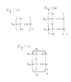
- Examples of the polymer are as follows: a single-chain-form of polysiloxane as shown in Figure 1 (a), a ladder-form of polysiloxane as shown in Figure 1 (b), and a polymer having a three dimensional structure of polysiloxane as shown in Figure 1 (c).
- R1 and R2 which are an organic group (a side chain group, i.e., a group presented at side chain group), and R3 and R4 which are an end group present in a repeating unit
- each of these groups can be a hydrogen atom, a hydroxyl group, a lower alkyl group having 1 to 5 carbon atoms, a lower alkoxyl group having 1 to 5 carbon atoms, a phenyl group, a benzyl group, a phenoxy group, a benzyloxy group, a trialkylsilyl group, etc.
- the condensation polymerization is caused by an anion or a cation produced from the sensitizing agent by exposure to light or radiation.
- the polymer having a siloxane-bond structure contains at least one side chain group or end group that is a functional group which causes this condensation polymerization.
- the functional group include a hydroxyl group, an alkoxyl group, or a phenoxy group.
- the polysilsesquioxane which is a particularly preferable material for resist, contains a hydroxyl group and an alkoxyl group in a ratio of 1 to 1 as an end group, and an alkyl group or a phenyl group as a side chain group.
- composition of the present invention comprising a base polymer consisting essentially of a polymer having a siloxane-bond and a sensitizing agent
- this resist will have sufficient sensitivity to light and small absorbance to ultraviolet rays, and therefore it is suitable for a lithography utilizing light of short wavelength.
- the resolving power of the resist can also be maintained and prevented from decreasing due to the deviation of the depth of the focus of light for use in exposure, thereby forming a fine resist pattern even on a substrate with a large difference in level.
- the polymer having a siloxane-bond structure undergoes condensation polymerization when irradiated with light or radiation and becomes insoluble in a solvent.
- the composition having sensitivity to light or radiation is used as a resist material by imparting polarity to the end group or the side chain group of the polymer having a siloxane-bond structure present in the composition
- an organic solvent not only an organic solvent but also an alkali solution can be used as a developer, which leads to a low cost developer, the easy disposal and the safe handling thereof, and no pollution.
- the use of an alkali solution may also prevent a resist from swelling, thereby preventing the resolution of a resist pattern from decreasing.
- the content of the polymer having a siloxane-bond structure of the composition is 10 percent by weight or more, and preferably 50 percent by weight or more.
- the resistance to dry etching of the composition decreases, thereby lowering the resolution of the transferred resist pattern.
- the above polymer having a siloxane-bond structure is used as a base polymer in the composition of the present invention, which may comprise a repeating unit such as styrene, a-methylstyrene, methylmethacrylate, methylacrylate, etc., in addition to.
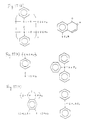
- the solution thus prepared is a solution of polymethylsilsesquioxane having a hydroxyl group as an end group as shown in Figure 1 (b), wherein R1 and R2 are a methyl group, and R3 and R4 are a hydroxyl group.
- Hydrolysis of a bifunctional silicon compound provides a chain of silicone shown in Figure 1 (a).
- hydrolysis and condensation of dimethyldichlorosilane provides polydimethylsiloxane which has a hydroxyl group as an end group as shown in Figure 1 (a), wherein R1 and R2 are a methyl group, and R3 is a hydroxyl group.
- Hydrolysis of a tetrafunctional silicon compound provides three dimensional silicone chain network as shown in Figure 1 (c).
- hydrolysis and condensation of tetrachlorosilane provides polysiloxane which has a hydroxyl group as an end group as shown in Figure 1 (c), wherein R3, and R4 are a hydroxyl group.
- any type of polysiloxane obtained have hydroxyl groups as end groups as shown in Figure 1, wherein R3 and R4 are a hydroxyl group.
- the functional group is an alkoxy group (in the above formula, an ethoxy group)
- a hydroxyl group and an alkoxy group are present each in almost the same amount as an end group of the resulting polysiloxane.
- a starting material may appropriately be selected to be polymerized so as to provide polysiloxane having the desired side chain groups, the desired end groups, and the desired framework of siloxane bonds according to objective thereof.
- a polymer having a siloxane-bond structure may be selected from a chain form, ladder form, or three dimensional form of polymer network, wherein a side chain group is a group represented by R1 and R2 shown in Figure 1, and an end group is a group represented by R3 and R4 shown in Figure 1.
- a substance which produces an acid or a substance which produces a radical when irradiated with light or radiation is used as a sensitizing agent present in the composition of the present invention.
- sensitizing agent an initiator or an acid producing agent
- sensitizing agent an initiator or an acid producing agent
- any compounds which produce acids when irradiated with light or radiation may be used.
- the compounds which produce acids by photolysis thereof described in U.S. patent No. 3,779,778 and Japanese Laid-Open Patent Publication No. 63-236028 may also be used in the composition of the present invention
- Onium salt produces a Br ⁇ nsted acid when irradiated with light or radiation.
- the onium salt include diaryliodonium salt (Ar 2 l + X - ),triarylsulfonium salt (Ar 3 S + X - ), triarylselenium salt (Ar 3 Se + X - ), wherein aryl (Ar) is mono- to tri- substituted or non-substituted benzene having a methyl group, a methoxy group, a t-butyl group, a nitro group, chlorine, or a CH 3 CONH- group, etc., as a substitution group, and an anion X - i s PF 6 - , AsF - 6 , SbF 6 - , BF 4 - , ClO 4 - , CF 3 SO 3 - , FSO 3 - , F 2 PO 2 - , etc.
- Aryldiazonium salt (ArN 2 X-) produces a Lewis acid when irradiated with light or radiation, wherein aryl (Ar) is mono- to tri- substituted or non-substituted benzene having a methyl group, a methoxy group, a morpholino group, a nitro group, chlorine, as a substitution group, and an anion X - is PF 5 - , AsF 6 - , SbF 6 - , BF 4 - , FeCl 4 - , SbCl 6 - , SnCl 6 - , etc.
- Sulfonate produces a sulfonic acid when irradiated with light or radiation, such as a-hydroxymethylben- zoinsulfonate, N-hydroxyimidosulfonate, a-sulfonyloxyketone, ⁇ -sulfonyloxyketone, p-nitrobenzyldiethoxyan- thracenesulfonate, o-nitrobenzyl tosylate, benzoin tosylate.
- a sulfonic acid when irradiated with light or radiation, such as a-hydroxymethylben- zoinsulfonate, N-hydroxyimidosulfonate, a-sulfonyloxyketone, ⁇ -sulfonyloxyketone, p-nitrobenzyldiethoxyan- thracenesulfonate, o-nitrobenzyl tosylate, benzoin tosylate.
- sensitizing agent which produces a radical when irradiated with light or radiation present in the composition of the present invention
- the sensitizing agent which produces a radical when irradiated with light or radiation present in the composition of the present invention
- examples of the sensitizing agent (the initiator) which produces a radical when irradiated with light or radiation present in the composition of the present invention include (1) to (3) described below. However, any compounds which produce radicals when irradiated with light or radiation may be used.
- Aromatic ketone such as benzophenone, thioxanthone, quinone, thioacridone, produces a radical when irradiated with light or radiation.
- Polyhalogenated hydrocarbon such as CBr 4 , CCI 4 , RCC1 3 , RCBr 3 , wherein R is a hydrogen atom, an alkyl group, an aryl group, or an aralkyl group, produces a radical when irradiated with light or radiation.
- a triazine compound (C 3 H 3 N 3 ), the 1 to 3 atoms of hydrogen moiety of which is substituted with a trichloromethyl group (CCIa-) also produces a radical when irradiated with light or radiation.
- CCIa- trichloromethyl group
- examples of the compound include 2,4,6-Tris(trichloromethyl)-1,3,5-triazine, 2,4-Bis(trichloromethyl)-6-(p-methoxyphenyl)-1,3,5-triazine), etc.
- composition of the present invention When the composition of the present invention is used as a resist material by adding the above sensitizing agent that produces on acid or a radical when irradiated with light or radiation thereto, the resulting acid or the radical catalyzes the condensation polymerization of the above polymer having a siloxane-bond structure.
- the content of the above sensitizing agent is preferably 40 percent by weight or less based on the weight of the base polymer.
- the sensitizing agent content is 40 percent by weight or less based on the weight of the base polymer, the resistance to dry etching of the composition decreases, thereby degrading the resolution of the transferred resist pattern.
- the content of the above sensitizing agent differs depending on the kind of light or radiation for use in exposure, when irradiated with an electron beam, the sensitizing agent content is preferably 10 percent by weight or less based on the weight of the base polymer, and when irradiated with ultraviolet rays, the sensitizing agent content is preferably in the range of 0.2 to 10 percent by weight based on the weight of the base polymer.
- Conventional process for forming a resist pattern comprises a step of forming a smoothing layer, a step of forming a resist film, a step of exposure, and a step of development.
- a smoothing layer is formed by a conventional method in order to level the uneven surface of a silicon substrate.
- the aforesaid composition having sensitivity to light or radiation is dissolved in an organic solvent to prepare a resist solution containing a solid in a concentration in the range of 5 to 50 percent by weight.
- the resist solution thus prepared is applied to the aforesaid leveled substrate by a spin coating process to form a film thereon. Then, the predetermined portions of the film are irradiated with light or radiation.
- the sensitizing agent in the irradiated portions produces an acid or a radical, which catalyzes a dehydration reaction or a de-alcoholization reaction of a polymer having a siloxane-bond structure as the other component of the resist film, thereby polymerizing the polymers.
- a developer capable of dissolving the pre-polymerization polymer having a siloxane-bond structure is used, the polymerized portions is insoluble in the developer, thereby forming a negative type of a resist pattern.
- the substrate is etched with suitable etchant, plasma, etc., to form a fine pattern reflecting the resist pattern.
- Hydrolysis and condensation of methyltriethoxysilane may provide polymethylsilsesquioxane as a base polymer.
- the number average molecular weight and the weight average molecular weight of the polymer are 1,310 and 3,320, respectively.
- the polymer is dissolved in an ethylalcohol/butylalcohol solvent mixture (weight ratio of ethylalcohol to butylalcohol is 1 : 1) to prepare a solution of 10 percent by weight. Thereafter, 1 to 5 percent by weight of triphenylsulfonium triflate is added as a sensitizing agent to the resulting solution based on the weight of the polymer to prepare a resist solution.
- Table 1 shows samples of the resist solution each having different concentration of a sensitizing agent therein.
- resist materials will now be each referred to as a sample 10, 11, 12, 13, or 15 according to the concentration of the sensitizing agent therein.
- the resist solution is applied to a silicon substrate by a spin coating process at a rate of 2,000 spin/min so that the resulting film has a thickness of 0.5 am.
- the resist film thus applied is dried by means of a hot plate at 75 C for 2 minutes, after which the predetermined pattern is drawn by means of an electron beam with an acceralation voltage of 25 kV or far ultraviolet rays utilizing a Xe-Hg lamp as light source (exposure energy: 25 mW/cm 2 ).
- exposure energy 25 mW/cm 2
- dip development dip development is conducted for 1 minute, which dissolves and removes the non-irradiated portions to form a resist pattern at the removed portions.
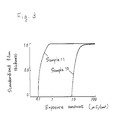
- Table 1 shows the sensitivity to an electron beam and the sensitivity to far ultraviolet rays of each sample containing a sensitizing agent in different concentration.
- Table 1 shows the measured values of the sensitivity to an electron beam and the sensitivety to far ultraviolet rays of the resist materials each containing a sensitizing agent in different concentration.
- the sensitivity to an electron beam and the sensitivity to far ultraviolet rays used herein are defined as exposure which may provide a film with a thickness of 50% of the initial film thickness.
- Figure 3 shows curve indicating the sensitivity to an electron beam of the samples 10 and 11 each containing a sensitizing agent in concentrations of 0% and 1 %, respectively.
- the resist formed in this example of the present invention is found to have much higher sensitivity.
- all the resist formed from the resist material of the samples 11, 12, 13, and 15 can resolve a line and space pattern having a width of 0.5 ⁇ m with exporue amount in the range of 0.18 to 0.3 ⁇ C/cm 2. The resolution is not found to be lowered due to swelling as is often found in the case of a negative type of resist.
- sample 10 that is a resist material containing no sensitizing agent may form a resist which has a sensitivity to an electron beam of 8 ⁇ C/cm 2 , which is as high as that of conventional resists.
- the resist which comprises only a base polymer without a sensitizing agent may independently serve as a resist material in the same manner as conventional resist materials.
- Sample 10 is a one-component resist material, has relatively high sensitivity to an electron beam and the high silicone content, and further can be developed by the use of an alkali developer, thereby serving as a resist material for an electron beam.
- the weight average molecular weight of the polymer present in the sample 10 is 3,320, and a 5% solution of TMAH is used as a developer.
- Figure 4 shows the relationship between the concentration of a TMAH aqueous solution and the dissolving rate of a polymer having a siloxane-bond structure (see Figure 2(a)) in the solution.
- the mark “*” denotes a sample of a polymer having a siloxane-bond structure having a molecular weight (Mw: weight average molecular weight) of 7,044, and a molecular weight distribution (Mn/Mw: the ratio of number average molecular weight to weight average molecular weight) of 2.1.
- Mw weight average molecular weight
- Mn/Mw the ratio of number average molecular weight to weight average molecular weight
- the mark “o” denotes a sample of the polymer having a molecular weight of 3,320 and a molecular weight distribution of 2.5.
- the mark “ ⁇ ” denotes a sample of the polymer having a molecular weight of 1,507 and a molecular weight distribution of 1.39.
- the dissolving rate of the polymer can be raised only when the concentration of the TMAH solution is raised. Therefore, when the concentration of the TMAH solution is held constant, the dissolving rate of the polymer decreases with a decrease in the molecular weight of the polymer. This phenomenon is largely different from the dissolving property of conventional polymers as a resist.
- the dissolving property shown in Figure 4 may be attributed to the chemical reaction between a TMAH solution and a polymer having a siloxane-bond structure.
- the polymer shown in Figure 2(a) does not simply dissolve in the TMAH solution.
- the condensation reaction of the polymers is effected because of the presence of a hydroxyl group and an ethoxy group both as an end group thereof by catalysis of TMAH which is an alkali compound. That is, the polymers dissolve in the TMAH solution, while partially becoming insoluble.
- a 2.38% solution of TMAH has been widely used as a developer for a photoresist. Therefore, a polymer which enables the development of the resist made of such polymer by the use of a 2.38% solution of TMAH may be used in the process without changing conventional equipments and conditions for manufacturing a semiconductor.
- the resist formed from a resist material containing the polymer having a siloxane-bond structure of the present invention is a negative type of resist. Thus, if the dissolving rate of the polymer is 20 nm/sec or more, the resist may serve as a negative type of resist.
- Figure 4 indicates that in order to obtain a dissolving rate of the polymer of 20 nm/sec or more under a 2.38% solution of TMAH, the molecular weight of 3,320 of the polymer having a siloxane-bond structure is too small to develop a resist.
- the weight average molecular weight of the polymer which serves as a base polymer is 7,044
- the dissolving rate of the polymer in the 2.38% solution of TMAH can be sufficiently raised. Consequently, when the weight average molecular weight of a polymer made of the framework of siloxane bonds is 7,044, the resist made of the polymer may be developed to serve as a negative type of resist.
- a resist comprising the polymer having a siloxane-bond structure having a weight average molecular weight of 7,044 as a base polymer may have the same relationship between the concentration of a sensitizing agent and the sensitivity of the resulting resist as that shown in Table 1.
- a polymer having a siloxane-bond structure having a weight average molecular weight of 1,507 has a glass transition point lower than room temperature, when the resist material containing such polymer is applied to a substrate to form a resist film, the resulting resist film exhibits viscosity. Therefore, a polymer having a siloxane-bond structure having a weight average molecular weight of 1,507 is not suitable for use as a base polymer. Consequently, in order to use the polymer having a weight average molecular weight of 1,500 or less as a base polymer, the resulting resist film requires heat treatment at high temperature, etc., so as to facilitate the condensation reaction thereof, thereby eliminating the viscosity.
- the weight average molecular weight of the polymer is preferably in the range of 2,000 to 100,000, and more preferably in the range of 3,000 to 50,000.
- the weight average molecular weight of the polymer of the present invention is preferably in the range of about 4,000 to about 20,000.
- Table 1 indicates that the resist formed in this example of the present invention has very high sensitivity to far ultraviolet rays in the range of 20 to 40 mJ/cm 2 .
- the resist formed in this example of the present invention has high sensitivity to an electron beam and far ultraviolet rays and high resolution.
- the onium salt used as a sensitizing agent of this example of the present invention has an absorption peak to ultraviolet rays at around 250 nm, and does not sensitize to light of a longer wavelength than 313 nm in the lower range of the absorption band thereof. Therefore, the resist has no sensitivity to a g-line (436 nm) and an i-line (365 nm) of a mercury lamp widely used at present in a process for manufacturing a semiconductor.
- the use of suitable organic dyes may impart the sensitivity of the resist to a g-line and an i-line.
- phenothiazine C1 2 Hg SN
- organic dyes For preparing such a resist, to the resist material of a sample 11 comprising 1 percent by weight of onium salt as a sensitizing agent is added 3 percent by weight of phenothiazine (C1 2 Hg SN) as organic dyes to raise the sensitivity. This improves the sensitivity to a g-line to 80 mJ/cm 2 , and the sensitivity to an i-line to 60 mJ/cm 2 .
- Phenothiazine is used as organic dyes for improving the sensitivity, because perylene as conventional organic dyes for improving the sensitivity is insoluble in a mixed solvent containing ethylalcohol and butylalcohol used as a solvent for the resist material, but phenothiazine has high solubility in such polar solvent.
- the onium salt used as a sensitizing agent when irradiated with light or radiation, the onium salt used as a sensitizing agent produces an acid.
- the de-ethylalcoholization reaction of the hydroxyl group and the ethoxy group both as an end group of polymethylsilsesquioxane used as a base polymer is effected by catalysis of the resulting acid, thereby facilitating the polymerization of the polymer.
- conventional polymerizable resists may serve as a negative type of resist by taking advantage of the property that same of the polymer constituting the resist becomes insoluble in a developer because of an increase in the molecular weight thereof when irradiated with light or radiation.
- the solubility of the resist of the present invention in an alkali aqueous solution is mainly attributed to the presence of a hydroxyl group as an end group of polymethylsilsesquioxane.
- the irradiated portions of the resist rapidly becomes insoluble in a developer because of the progress of the reaction shown in Figure 5(b).
- the irradiated portions of the resist of the present invention becomes insoluble because of an increase in the molecular weight, together with a change in the polarity of the polymers at the irradiated portion. This may markedly increase a difference in the dissolving rate between the irradiated portions and the non-irradiated portions. Consequently, the resist of the present invention has a characteristic of very high sensitivity and high contrast property.
- the number average molecular weight and the weight average molecular weight of the base polymer herein used are 1,310 and 3,320, respectively. Not limited to the present example, the weight average molecular weight of the polymer may preferably be in the range of 2,000 to 500,000, and more preferably in the range of 3,000 to 100,000.
- the molecular weight distribution i,e., the value obtained by dividing the weight average molecular weight by the number average molecular weight, is 2.5 in this example. However, it is desirable that the molecular weight distribution be close to 1 as much as possible.
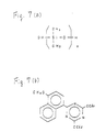
- Figure 6 shows the resist materials of Example 2.
- polydiphenylsilsesquioxane having a siloxane-bond structure shown in Figure 6(a) comprising a phenyl group as a side chain group and a hydroxyl group and an ethoxy group as an end group is a base polymer.
- Diphenyliodonium fluoroantimonate shown in Figure 6(b) is a sensitizing agent (an initiator)
- perylene (C28 H18) shown in Figure 6(c) is used as a sensitizer.
- a resist material containing no sensitizing agent will be referred to as a sample 20, and a resist material containing a sensitizing agent and a sensitizer each in an amount of 1 percent by weight will be referred to as a sample 21 hereinafter.
- the number average molecular weight and the weight average molecular weight of the polymer are 1,900 and 3,420, respectively.
- the above polymer is dissolved in butyl acetate to prepare a 10 wt% solution. Then, to the resulting solution is added 1 percent by weight of diphenylsulfoniumfluoroantimonate as a sensitizing agent and 1 percent by weight of perylene based on the weight of the polymer to prepare a resist solution.
- the resist solution is applied to a silicon substrate by a spin coating process at a rate of 2,200 spin/min so that the resulting resist film has a thickness of 0.5 am.
- the resist film thus applied is dried by means of a hot plate at 75 C for 2 minutes, after which by the use of a stepper utilizing a g-line as light source (exposure wavelength: 436 nm, the numerical apeture of a lens: 0.45) or a stepper utilizing an i-line as light source (exposure wavelength: 365 nm, the numerical apeture of a lens: 0.40), the resist film is exposed to ultraviolet rays through a photomask having a predetermined light non-transmissive pattern.
- Sample 21 has a sensitivity to a g-line of 12 mJ/cm 2 and a sensitivity to an i-line of 45 mJ/cm 2 .
- the resist made of the resist material of the present invention may also have very high sensitivity to ultraviolet rays (g-line, i-line) owing to the use of a sensitizer. Both exposures above can provide a line and space resist pattern with a width of 0.8 ⁇ m.
- development is conducted by the use of an organic solvent, but may also be conducted by the use of a TMAH aqueous solution.
- Figure 7 shows resist materials of Example 3.
- polydimethylsiloxane having a siloxane-bond structure comprising a methyl group as a side chain group and a hydroxyl group as an end group is used as a base polymer.
- 2-(4'-methoxy-1'-naphtyl)-4,6-bis(trichloromethyl)-1,3,5-triazine shown in Figure 6(b) is a sensitizing agent (an initiator).
- the above polymer is dissolved in butylalcohol/ethylalcohol mixed solvent (weight ratio of butylalcohol to ethylalcohol is 1:1) to prepare a 10 wt% solution. Then, to the resulting solution is added 1 percent by weight based on the weight of the polymer-of the above triazine compound as a sensitizing agent to prepare a resist solution.
- the resist solution is applied to a silicon substrate by a spin coating process at a rate of 1,700 spin/min so that the resulting resist film has a thickness of 0.5 am.
- the resist film is dried by means of a hot plate at 75 C for 2 minutes, after which by the use of a stepper utilizing an i-line as light source (exposure wavelength: 365 nm, the numerical apeture of a lens: 0.40), the resist film is exposed to ultraviolet rays through a photomask with a predetermined pattern.
- the radiation energy during exposure to ultraviolet rays is 250 mW/cm 2 .
- TMAH 2.38% solution of TMAH as a developer
- dip development is conducted for 1 minute.
- the sensitivity to an i-line of this resist is 33 mJ/cm 2.
- the above exposure may also provide a line and space resist pattern with a width of 1 am.
- Figure 8 shows resist materials of Example 4.
- polyhydroxybenzylsilsesquioxane having a siloxane-bond structure comprising a hydroxybenzyl group as a side chain group and a hydroxyl group as an end group as shown in Figure 8-(a) is used as a base polymer
- o-Nitrobenzyl tosylate shown in Figure 8(b) is a sensitizing agent (an initiator).
- the above polymer is dissolved in butylalcohol/ethylalcohol mixed solvent (weight ratio of butylalcohol to ethylalcohol is 1:1) to prepare a 10 wt% solution. Then, to the resulting solution is added 1 percent by weight based on the weight of the polymer of the above nitrobenzyl tosylate as a sensitizing agent to prepare a resist solution.
- the resist solution is applied to a silicon substrate by a spin coating process at a rate of 2,100 spin/min so that the resulting resist film has a thickness of 0.5 am.
- the resist film is dried by means of a hot plate at 75 C for 2 minutes, after which by the use of an aligner utilizing a Xe-Hg lamp as light source, the resist film is exposed to ultraviolet rays through a photomask with a predetermined pattern.
- the radiation energy during exposure to ultraviolet rays is 250 mW/cm 2.
- TMAH dip development is conducted for 1 minute.
- the sensitivity to an i-line of this resist is 60 mJ/cm 2.
- the above exposure provides a line and space resist pattern with a width of 1 am.
- the base polymer having a weight average molecular weight of about 3,000 is described.
- the weight average molecular weight is not limited to this Example, it is preferably in the range of 500 to 500,000, and more preferably in the range of 1,000 to 100,000.
- the weight average molecular weight needs to be restricted up to about 10,000.
- the molecular weight distribution i.e., the value obtained by dividing the weight average molecular weight by the number average molecular weight is desirably close to 1 as much as possible.
- a sensitizing agent is contained in a concentration range of 0 to 5 percent by weight based on the weight of the base polymer.
- the concentration of sensitizing agent may practically be in the range of 0 to 40 percent by weight.
- the concentration of sensitizing agent is high, the silicon content of the resist film decreases, which entails a problem in that the resistance to plasma etching is decreased as shown in Figure 9. Since the polymer having a siloxane-bond structure has excellent property as described below, it is desirable that the concentration of the sensitizing agent may be lowered as much as possible in order to raise the polymer content of the resist film.
- the polymer may have sufficient sensitivity to an electron beam even with no sensitizing agent contained, thereby being able to be used independently as a resist.
- a problem arises in that the sensitivity to ultraviolet rays or far ultraviolet rays markedly decreases when the concentration of the sensitizing agent content is 0.2% by weight or less based on the weight of a base polymer. Therefore, it is necessary to vary the concentration of the sensitizing agent according to the end use thereof.
- the property of the resist is decided upon the balance between the sensitivity to light or radiation and the silicon content of the resist.
- the concentration of sensitizing agent in the range of 0 to 10 percent by weight based on the weight of a base polymer is very effective as a resist, while when used as a resist for ultraviolet rays, the range of 0.2 to 10 percent by weight based on the weight of a base polymer is very effective as a resist.
- composition having no sensitizing agent has sufficient sensitivity for use as a resist for an electron beam. Therefore, unless very high sensitivity is required, it is effective to use a base polymer containing no sensitizing agent as a one-component resist so that the excellent property of the polymer may be fully utilized.
- the resist material of the present invention has the high silicone content as shown in Figure 9.
- the resist material (sample 11) shown in Figure 2 has the silicone content close to that of a silicon dioxide film (Si0 2 ), thereby providing high resistance to plasma. This may improve the selection ratio during a process of etching, and therefore a resist pattern may be transferred with high resolution.
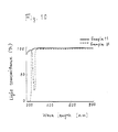
- Figure 10 shows the light transmittance of the resist material of the present invention, wherein the full line represents the light transmittance of a sample 11 with a film thickness of 1 am, and the broken line denotes the light transmittance of a sample 21 with a film thickness of 1 am.
- Sample 21 has high light transmittance in a wide range from visible light to medium ultraviolet rays while absorbing light of e wavelength of 300 nm or less according to a phenyl group thereof.
- sample 11 has high light transmittance of all the range from visible light to far ultraviolet rays.
- the resist material of the present invention has high light transmittance. This is attributed to the fact that the base polymer made of a framework of the siloxane bonds has high light transmittance to ultraviolet rays and that the concentration of sensitizing agent can be restricted to a lower concentration degree because the resist material utilizes the chemically sensitizable reaction.
- Figure 11 shows the results of thermogravimetric analysis, wherein the full line represents the value of sample 11 with a film thickness of 1 ⁇ m, and the broken line denotes the value of polyimide with a film thickness of 1 ⁇ m.
- the weight of sample 11 scarcely decreases at temperatures up to 500 C, and slightly decreases even at 500 C or more. This decrease in weight of the sample occurs because the methyl groups at the side chains groups are dissociated from the polymer of the sample.
- Polyimide has been widely used as conventional heat-resistant polymer material.
- Figure 11 clearly shows that the resist of the present invention has higher heat resistance compared with polyimide.
- Sample 11 is used to prepare a resist pattern by exposure and development. The resulting resist pattern is heated, after which the thermal deformation of the resist pattern is observed. However, at temperatures up to 300 C, no thermal deformation of the resist pattern can be observed.
- the resist pattern of a conventional photoresist begins to deform at about 120°C. Consequently, the resist pattern of the present invention is found to possess remarkably high thermal resistance.
- the resist of the present invention is mainly composed of polysiloxane, it has high electrical insulating property, high hardness, excellent water resisting property, low hygroscopic property, high adhesion to a metal substrate or a silicon substrate, and further high capability of leveling the uneven surface of a substrate.
- the composition having sensitivity to light or radiation of the present invention has sensitivity to light, together with high plasma resistance, high light transmittance, high thermal resistance, high electrical insulating property, high hardness, high water resisting property, low hygroscopic property, high adhesion, and high smoothing capability. Therefore, the resist has not only a use for a resist material for preparing fine elements but also various other uses.
- composition having sensitivity to light or radiation of the present invention is used as a resist material.
- composition having sensitivity to light or radiation of the present invention is used as an upper resist in a two-layer resist method for an electron beam lithography.
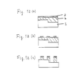
- a polyimide with a thickness of 2 I .Lm. Thereafter, the polyimide film is heat treated at 200 C to form a smoothing layer 2, to which is applied the resist material of the present invention with a thickness of 0.25 ⁇ m ( Figure 12(a)).
- the resist material shown in Figure 2 is used wherein polymethylsilsesquioxane having a siloxane-bond structure which contains a methyl group as a side chain group and a hydroxyl group and an ethoxy group as an end group is a base polymer, and triphenylsulfoniumtriflate is a sensitizing agent.
- the number average molecular weight and the weight average molecular weight of polymethylsilsesquioxane are 3,273 and 7,044, respectively, and the concentration of sensitizing agent content is 2 percent by weight.
- the predetermined portions of the resist film are exposed to an electron beam at an exposure amount of 0.3 u.C/cm 2 , after which the resist is developed in a 2.38% solution of TMAH ( Figure 12(b)).
- the smoothing layer 2 is etched by means of dry etching by the use of oxygen.
- an upper layer with a resist pattern is used as a mask for dry etching, and the pattern at the predetermined portions exposed to an electron beam is transferred to the lower smoothing layer 2 ( Figure 12(c)).
- This method may provide a pattern with a width of 0.3 ⁇ m on a semiconductor substrate having a difference in level of 1 ⁇ m by a low exposure amount rate of 0.3 u.C/cm 2 .
- the phase shifting mask is obtained by improving a photomask for use in exposure by means of a conventional projection and exposure apparatus in order to form a fine pattern.
- a method is for forming a finer resist pattern by imparting a phase difference to light from an optimal system which is used in exposure. Examples of the method utilizing such a photomask (hereinafter, referred to as a phase shifting mask) are described in Japanese Laid-Open Patent Publication No. 62-50811, Japanese Laid-Open Patent Publication No. 62-59296, etc.
- the original picture of a pattern to be transferred to a photomask substrate is made of a light non-transmissive film.
- a phase shifter having a pattern on a transparent film is provided on either of transparent portions having a pattern. These transparent portions hold the light non-transmissive film between them or are formed at both sides of the light non-transmissive film.
- the phase shifter changes the phase of light to be exposured.
- phase shifter for use in a conventional photomask needs to be transparent with respect to light having wavelength upto that of ultraviolet rays.
- the phase shifter On handling the photomask, it is desirable that the phase shifter has high hardness, and high resistance to shock, and furthermore, has excellent thermal resistance and chemical resistance for washing thereof when dust, etc., deposit thereover.
- the phase shifter is required to have high water resisting property, low hygroscopic property, and high adhesion to a substrate, concerning washing.
- phase shifter The process for forming a phase shifter will now be described, wherein the composition having sensitivity to light or radiation of the present invention is used as a resist material.
- Figure 13(a) shows a photomask comprising a chrome film with a pattern 5 on a quartz substrate 4.
- polymethylsilsesquioxane having a siloxane-bond structure which contains a methyl group as a side chain group and a hydroxyl group and an ethoxy group as an end group is used as a resist material.
- the weight average molecular weight of this resist material is 7,044.
- the resist material containing no sensitizing agent is used so as to avoid the absorption of ultraviolet rays by the sensitizing agent.
- This resist film is heat treated at 70 C, after which the treated film is exposed to an electron beam at a rate of 25 u.C/cm 2 , and then developed by the use of a 2.38% solution of TMAH to form a resist pattern ( Figure 13(c)).
- this mask substrate at 200 C completes the reaction of the end group of the pre-polymerization polymer (-OH, -C 2 H s OH),thereby stabilizing the resist.
- the resist thus prepared is used as a phase shifter 6.
- this resist is transparent to light having wavelength up to that of ultraviolet rays, and has high thermal resistance and chemical resistance, and concerning washing has further properties of high water resisting property, low hygroscopic property, and high adhesion to a substrate.
- the phase shifting mask may be prepared in a easy process as shown in Figure 13.
- Figure 14 shows the construction of another phase shifting mask by the use of the resist of the present invention as a phase shifter.
- Figure 14(a) shows a Levenson type phase shifting mask comprising the phase shifter 6 arrayed at every other groove of the chrome film with a pattern 5.
- Figure 14(b) shows a transparent type phase shifting mask comprising only a phase shifter 6 which has a pattern formed by said phase shifter.
- Figure 14(c) shows an emphasized-edge type phase shifting mask comprising the phase shifter 6 arrayed at a predetermined distance from the groove of the chrome film with a pattern 5.
- a silicon dioxide film (Si0 2 ) or a coated oxide film (SOG) has been used as the phase shifter of a phase shifting mask.
- a resist pattern is formed on a silicon dioxide film or a SOG film, and by the use of the resulting resist pattern as a mask, a phase shifting pattern is formed by dry etching.
- This conventional method involves a complicated manufacturing process, accompanied with increased defective density
- the pattern of the phase shifter 6 can be directly drawn by means of an electron beam, thereby largely simplifying the process for preparing a phase shifting mask.
- composition having sensitivity to light or radiation of the present invention is used as a chip covering material of a semiconductor device will now be described in detail by reference to Figure 15.
- semiconductor elements are provided on the silicon substrate 1. All the surface of a silicon substrate 1 except the portions where bonding pads 8 made of an aluminium film is formed, is covered by a silicon nitride film used as a protective coat 7, thereby opening windows of the protective coat at the bonding pad portions.
- the resist material of the present invention is applied to this coated substrate 1 with a thickness of 3.5 ⁇ m, after which the resulting film is heat treated at 70 C ( Figure 15(b)).
- a composition is used as a resist material, wherein polyphenylsilsesquioxane having a siloxane-bond structure which contains a phenyl group as a side chain group and a hydroxyl group and an ethoxy group as an end group is a base polymer, diphenyliodoniumfluoroantimonate is a sensitizing agent, and perylene is a sensitizer.
- the resist film is exposed to light by means of a stepper utilizing a g-line at a exposure amount of 60 mJ/cm 2 , after which the irradiated film is developed by the use of a 5% TMAH solution to leave the resist film on the circuit portions on the semiconductor substrate 1 ( Figure 15(c)).
- an open window at the bonding pads 8 on the substrate 1 is connected to gold wires 9 by wire- bonding, thereby completing a semiconductor device.
- this resist material has high thermal resistance as well as high chemical resistance, it may be directly used as a chip covering material.
- Polyimide has been used as a conventional chip covering material.
- a resist pattern should be formed on the polyimide film, and then the polyimide film should be etched by means of wet etching through the resist pattern as a mask.
- the use of the resist material of the present invention as a chip covering material enables a window to be opened by exposure to ultraviolet rays, thereby largely simplifying the process.
- this resist has high transparency to light including ultraviolet rays as stated above, it is particularly effective as a window material for EPROM (erasable programmable read-only memory) wherein data is erased by irradiation with ultraviolet rays.
- EPROM erasable programmable read-only memory
- composition having sensitivity to light or radiation of the present invention may be applied for various materials besides a resist material for use in an upper resist film of a two-layer resist, a chip covering material on a protective coat of a semiconductor device, a material for constituting a phase shifting film for a phase shifting mask.
- the composition of the present invention may be used as a material of a micro lens for use in converging light from CCD, a material for constituting an a-rays cutoff film of a semiconductor element, a protective coat material of a semiconductor device, a layer insulation film material for multilayer inter-connection, a smoothing layer material for multilayer inter-connection of a semiconductor device, a smoothing material of a babble memory device, an insulating layer material of a thin film magnetic head, etc.
- a pattern may be directly formed by exposure as mentioned in Examples, and it is necessary to denote that the resulting pattern has high resistance to plasma, high transparency, high thermal resistance, high electric insulating property, high hardness, high water resisting property, low hygroscopic property, high adhesion to substrate, high smoothing capability, etc.
- the Examples mentioned above illustrate the exposure of predetermined pattern to ultraviolet rays or an electron beam.
- the light source is not limited to those used in the Examples, the use of an ion beam or an X-ray may be possible.
Landscapes
- Physics & Mathematics (AREA)
- Spectroscopy & Molecular Physics (AREA)
- General Physics & Mathematics (AREA)
- Exposure And Positioning Against Photoresist Photosensitive Materials (AREA)
Applications Claiming Priority (3)
| Application Number | Priority Date | Filing Date | Title |
|---|---|---|---|
| JP16717390 | 1990-06-25 | ||
| JP167173/90 | 1990-06-25 | ||
| JP16717390 | 1990-06-25 |
Publications (3)
| Publication Number | Publication Date |
|---|---|
| EP0464614A2 true EP0464614A2 (de) | 1992-01-08 |
| EP0464614A3 EP0464614A3 (en) | 1992-09-02 |
| EP0464614B1 EP0464614B1 (de) | 1999-09-29 |
Family
ID=15844774
Family Applications (1)
| Application Number | Title | Priority Date | Filing Date |
|---|---|---|---|
| EP91110509A Expired - Lifetime EP0464614B1 (de) | 1990-06-25 | 1991-06-25 | Licht- oder strahlungsempfindliche Zusammensetzung |
Country Status (4)
| Country | Link |
|---|---|
| US (3) | US5378585A (de) |
| EP (1) | EP0464614B1 (de) |
| KR (1) | KR950002874B1 (de) |
| DE (1) | DE69131658T2 (de) |
Cited By (2)
| Publication number | Priority date | Publication date | Assignee | Title |
|---|---|---|---|---|
| US5378585A (en) * | 1990-06-25 | 1995-01-03 | Matsushita Electronics Corporation | Resist composition having a siloxane-bond structure |
| WO2008093629A1 (ja) * | 2007-02-01 | 2008-08-07 | Tokyo Ohka Kogyo Co., Ltd. | 液晶表示素子用平坦化絶縁膜形成用組成物および液晶表示素子用平坦化絶縁膜の製造方法 |
Families Citing this family (48)
| Publication number | Priority date | Publication date | Assignee | Title |
|---|---|---|---|---|
| JP2934353B2 (ja) * | 1992-06-24 | 1999-08-16 | 三菱電機株式会社 | 半導体装置およびその製造方法 |
| TW434458B (en) * | 1995-04-04 | 2001-05-16 | Shinetsu Chemical Co | Chemically amplified positive resist compositions |
| JP2697680B2 (ja) * | 1995-05-31 | 1998-01-14 | 日本電気株式会社 | 珪素含有高分子化合物および感光性樹脂組成物 |
| KR970011972A (ko) * | 1995-08-11 | 1997-03-29 | 쯔지 하루오 | 투과형 액정 표시 장치 및 그 제조 방법 |
| JPH1160735A (ja) * | 1996-12-09 | 1999-03-05 | Toshiba Corp | ポリシランおよびパターン形成方法 |
| WO1998040439A1 (en) * | 1997-03-14 | 1998-09-17 | Minnesota Mining And Manufacturing Company | Cure-on-demand, moisture-curable compositions having reactive silane functionality |
| US6372415B1 (en) * | 1997-10-30 | 2002-04-16 | Kao Corporation | Resist developer |
| JP3796982B2 (ja) * | 1998-06-02 | 2006-07-12 | 住友化学株式会社 | ポジ型レジスト組成物 |
| US6087064A (en) * | 1998-09-03 | 2000-07-11 | International Business Machines Corporation | Silsesquioxane polymers, method of synthesis, photoresist composition, and multilayer lithographic method |
| JP3120402B2 (ja) | 1998-09-03 | 2000-12-25 | インターナショナル・ビジネス・マシーンズ・コーポレ−ション | 不活性化芳香族アミン化合物を含むフォトレジスト組成物 |
| TWI221946B (en) | 1999-01-07 | 2004-10-11 | Kao Corp | Resist developer |
| US6136511A (en) * | 1999-01-20 | 2000-10-24 | Micron Technology, Inc. | Method of patterning substrates using multilayer resist processing |
| TW497165B (en) * | 1999-06-30 | 2002-08-01 | Hitachi Ltd | Method for manufacturing semiconductor integrated circuit device, optical mask used therefor, method for manufacturing the same, and mask blanks used therefor |
| US6361904B1 (en) | 2000-06-14 | 2002-03-26 | Taiwan Semiconductor Manufacturing Company | Method for repairing the shifter layer of an alternating phase shift mask |
| US6420084B1 (en) | 2000-06-23 | 2002-07-16 | International Business Machines Corporation | Mask-making using resist having SIO bond-containing polymer |
| JP3760086B2 (ja) * | 2000-07-07 | 2006-03-29 | 株式会社ルネサステクノロジ | フォトマスクの製造方法 |
| TW541605B (en) * | 2000-07-07 | 2003-07-11 | Hitachi Ltd | Fabrication method of semiconductor integrated circuit device |
| JP2002184669A (ja) | 2000-12-14 | 2002-06-28 | Hitachi Ltd | 半導体集積回路装置の製造方法 |
| JP2002196470A (ja) | 2000-12-26 | 2002-07-12 | Hitachi Ltd | フォトマスクの製造方法および半導体集積回路装置の製造方法 |
| JP2002202585A (ja) | 2000-12-27 | 2002-07-19 | Hitachi Ltd | フォトマスクの製造方法および半導体集積回路装置の製造方法 |
| US6617674B2 (en) | 2001-02-20 | 2003-09-09 | Dow Corning Corporation | Semiconductor package and method of preparing same |
| EP1364917A4 (de) * | 2001-03-01 | 2006-03-15 | Nippon Sheet Glass Co Ltd | Verfahren zur herstellung optischer elemente |
| US6731857B2 (en) | 2001-03-29 | 2004-05-04 | Shipley Company, L.L.C. | Photodefinable composition, method of manufacturing an optical waveguide with the photodefinable composition, and optical waveguide formed therefrom |
| US6589711B1 (en) * | 2001-04-04 | 2003-07-08 | Advanced Micro Devices, Inc. | Dual inlaid process using a bilayer resist |
| TW594416B (en) * | 2001-05-08 | 2004-06-21 | Shipley Co Llc | Photoimageable composition |
| JP3827544B2 (ja) | 2001-08-31 | 2006-09-27 | 株式会社ルネサステクノロジ | 半導体集積回路装置の製造方法 |
| JP2003121977A (ja) * | 2001-10-12 | 2003-04-23 | Hitachi Ltd | 半導体集積回路装置の製造方法およびマスク |
| JP2003287875A (ja) * | 2002-01-24 | 2003-10-10 | Hitachi Ltd | マスクの製造方法および半導体集積回路装置の製造方法 |
| JP3754378B2 (ja) * | 2002-02-14 | 2006-03-08 | 株式会社ルネサステクノロジ | 半導体集積回路装置の製造方法 |
| JP4557497B2 (ja) * | 2002-03-03 | 2010-10-06 | ローム・アンド・ハース・エレクトロニック・マテリアルズ,エル.エル.シー. | シランモノマー及びポリマーを製造する方法及びそれを含むフォトレジスト組成物 |
| JP2004038142A (ja) | 2002-03-03 | 2004-02-05 | Shipley Co Llc | ポリシロキサンを製造する方法及びそれを含むフォトレジスト組成物 |
| JP2004212946A (ja) * | 2002-10-21 | 2004-07-29 | Rohm & Haas Electronic Materials Llc | Siポリマー含有フォトレジスト |
| EP1422565A3 (de) * | 2002-11-20 | 2005-01-05 | Shipley Company LLC | Mehrlagige Fotoresist-Systeme |
| KR20040044368A (ko) * | 2002-11-20 | 2004-05-28 | 쉬플리 캄파니, 엘.엘.씨. | 다층 포토레지스트 시스템 |
| US6842577B2 (en) * | 2002-12-02 | 2005-01-11 | Shipley Company L.L.C. | Photoimageable waveguide composition and waveguide formed therefrom |
| JP2004185000A (ja) * | 2002-12-02 | 2004-07-02 | Rohm & Haas Electronic Materials Llc | 導波路を形成する方法及びそれから形成される導波路 |
| US20040229159A1 (en) * | 2003-02-23 | 2004-11-18 | Subbareddy Kanagasabapathy | Fluorinated Si-polymers and photoresists comprising same |
| KR101112482B1 (ko) * | 2003-03-03 | 2012-02-24 | 롬 앤드 하스 일렉트로닉 머트어리얼즈, 엘.엘.씨. | Si-폴리머 및 이를 포함하는 포토레지스트 |
| US7072564B2 (en) * | 2003-11-25 | 2006-07-04 | Rohm And Haas Electronic Materials Llc | Waveguide compositions and waveguides formed therefrom |
| JP5102428B2 (ja) * | 2003-11-25 | 2012-12-19 | ローム・アンド・ハース・エレクトロニック・マテリアルズ,エル.エル.シー. | 導波路組成物およびこれから形成された導波路 |
| EP1586603B1 (de) * | 2004-04-14 | 2007-06-13 | Rohm and Haas Electronic Materials LLC | Zusammensetzungen für Wellenleiter und daraus hergestellte Wellenleiter |
| KR100593042B1 (ko) | 2004-09-07 | 2006-06-26 | 안성화인케미칼 주식회사 | 고개구율 액정표시소자의 유기절연막 형성용 음성레지스트 조성물 |
| US7659050B2 (en) * | 2005-06-07 | 2010-02-09 | International Business Machines Corporation | High resolution silicon-containing resist |
| JP4699140B2 (ja) * | 2005-08-29 | 2011-06-08 | 東京応化工業株式会社 | パターン形成方法 |
| JP2007211062A (ja) * | 2006-02-07 | 2007-08-23 | Tokyo Ohka Kogyo Co Ltd | 着色シリカ系被膜形成用組成物 |
| US7939236B2 (en) * | 2007-02-22 | 2011-05-10 | Lexmark International, Inc. | Chemically prepared toner and process therefor |
| US20100255427A1 (en) * | 2009-04-02 | 2010-10-07 | Taiwan Semiconductor Manufacturing Company, Ltd. | Conformal photo-sensitive layer and process |
| KR102375191B1 (ko) * | 2015-01-05 | 2022-03-17 | 삼성디스플레이 주식회사 | 포지티브형 감광성 실록산 수지 조성물 및 이를 포함하는 표시 장치 |
Family Cites Families (23)
| Publication number | Priority date | Publication date | Assignee | Title |
|---|---|---|---|---|
| US3779778A (en) * | 1972-02-09 | 1973-12-18 | Minnesota Mining & Mfg | Photosolubilizable compositions and elements |
| JPS5760330A (en) * | 1980-09-27 | 1982-04-12 | Fujitsu Ltd | Resin composition |
| DE3278567D1 (en) * | 1981-10-03 | 1988-07-07 | Japan Synthetic Rubber Co Ltd | Solvent-soluble organopolysilsesquioxanes, processes for producing the same, and compositions and semiconductor devices using the same |
| US4442197A (en) * | 1982-01-11 | 1984-04-10 | General Electric Company | Photocurable compositions |
| DE3374452D1 (en) * | 1982-04-05 | 1987-12-17 | Ibm | Method of increasing the image resolution of a transmitting mask and improved masks for performing the method |
| US4491628A (en) * | 1982-08-23 | 1985-01-01 | International Business Machines Corporation | Positive- and negative-working resist compositions with acid generating photoinitiator and polymer with acid labile groups pendant from polymer backbone |
| JPS5968735A (ja) * | 1982-10-13 | 1984-04-18 | Tokyo Ohka Kogyo Co Ltd | 感光性組成物 |
| JPS6052845A (ja) * | 1983-09-02 | 1985-03-26 | Japan Synthetic Rubber Co Ltd | パタ−ン形成材料 |
| JPS61144639A (ja) * | 1984-12-19 | 1986-07-02 | Hitachi Ltd | 放射線感応性組成物及びそれを用いたパタ−ン形成法 |
| US4759616A (en) * | 1985-08-26 | 1988-07-26 | Eastman Kodak Company | Method and apparatus for anamorphically shaping and deflecting electromagnetic beams |
| JPS6259296A (ja) * | 1985-09-10 | 1987-03-14 | Green Cross Corp:The | ペプタイド誘導体 |
| US4665006A (en) * | 1985-12-09 | 1987-05-12 | International Business Machines Corporation | Positive resist system having high resistance to oxygen reactive ion etching |
| DE3760030D1 (en) * | 1986-02-07 | 1989-02-02 | Nippon Telegraph & Telephone | Photosensitive and high energy beam sensitive resin composition containing substituted polysiloxane |
| JPS6346094A (ja) * | 1986-08-13 | 1988-02-26 | Matsushita Electric Ind Co Ltd | 構内電子交換機 |
| JPS63236028A (ja) * | 1987-03-25 | 1988-09-30 | Fuji Photo Film Co Ltd | 光可溶化組成物 |
| JPS63279245A (ja) * | 1987-05-12 | 1988-11-16 | Fujitsu Ltd | ネガ型レジスト組成物 |
| JPH07102439B2 (ja) * | 1988-07-04 | 1995-11-08 | 宇部興産株式会社 | ロータリダイカストマシンの回転テーブル駆動制御方法 |
| JP2608429B2 (ja) * | 1987-11-09 | 1997-05-07 | 東レ・ダウコーニング・シリコーン株式会社 | パターン形成用材料およびパターン形成方法 |
| JPH0815650B2 (ja) * | 1988-07-04 | 1996-02-21 | 宇部興産株式会社 | 加圧鋳造方法 |
| US5059512A (en) * | 1989-10-10 | 1991-10-22 | International Business Machines Corporation | Ultraviolet light sensitive photoinitiator compositions, use thereof and radiation sensitive compositions |
| JP2646289B2 (ja) * | 1990-06-01 | 1997-08-27 | 富士写真フイルム株式会社 | レジスト組成物 |
| EP0464614B1 (de) * | 1990-06-25 | 1999-09-29 | Matsushita Electronics Corporation | Licht- oder strahlungsempfindliche Zusammensetzung |
| EP0568476B1 (de) * | 1992-04-30 | 1995-10-11 | International Business Machines Corporation | Silikon enthaltendes positives Photoresistmaterial und dessen Verwendung in Dünnfilm-Verpackung-Technologie |
-
1991
- 1991-06-25 EP EP91110509A patent/EP0464614B1/de not_active Expired - Lifetime
- 1991-06-25 DE DE69131658T patent/DE69131658T2/de not_active Expired - Fee Related
- 1991-06-25 KR KR1019910010558A patent/KR950002874B1/ko not_active Expired - Fee Related
-
1993
- 1993-10-13 US US08/135,952 patent/US5378585A/en not_active Expired - Lifetime
-
1994
- 1994-09-09 US US08/304,086 patent/US5547808A/en not_active Expired - Lifetime
-
1995
- 1995-05-23 US US08/448,100 patent/US5554465A/en not_active Expired - Lifetime
Cited By (2)
| Publication number | Priority date | Publication date | Assignee | Title |
|---|---|---|---|---|
| US5378585A (en) * | 1990-06-25 | 1995-01-03 | Matsushita Electronics Corporation | Resist composition having a siloxane-bond structure |
| WO2008093629A1 (ja) * | 2007-02-01 | 2008-08-07 | Tokyo Ohka Kogyo Co., Ltd. | 液晶表示素子用平坦化絶縁膜形成用組成物および液晶表示素子用平坦化絶縁膜の製造方法 |
Also Published As
| Publication number | Publication date |
|---|---|
| US5378585A (en) | 1995-01-03 |
| US5547808A (en) | 1996-08-20 |
| EP0464614B1 (de) | 1999-09-29 |
| US5554465A (en) | 1996-09-10 |
| KR950002874B1 (ko) | 1995-03-27 |
| DE69131658D1 (de) | 1999-11-04 |
| DE69131658T2 (de) | 2000-04-27 |
| EP0464614A3 (en) | 1992-09-02 |
Similar Documents
| Publication | Publication Date | Title |
|---|---|---|
| US5378585A (en) | Resist composition having a siloxane-bond structure | |
| EP0758102B1 (de) | Terpolymere mit Organosiliziumseitenketten und ihre Verwendung zur Herstellung von Reliefstrukturen | |
| JP3340864B2 (ja) | ポジ型化学増幅レジスト組成物 | |
| US6884571B2 (en) | Intermediate layer composition for three-layer resist process and pattern formation method using the same | |
| US6913865B2 (en) | Surface modified encapsulated inorganic resist | |
| US5338818A (en) | Silicon containing positive resist for DUV lithography | |
| JP2004212946A (ja) | Siポリマー含有フォトレジスト | |
| US5035979A (en) | Radiation-sensitive mixture | |
| US6399792B2 (en) | Photoresist cross-linker and photoresist composition comprising the same | |
| JP3293940B2 (ja) | 感光性組成物及びそれを用いたパターン形成方法 | |
| JPH09258448A (ja) | レジスト組成物及びそれを用いた半導体装置製造方法 | |
| JPH0262544A (ja) | フォトレジスト組成物 | |
| JPH07113773B2 (ja) | パタ−ン形成方法 | |
| JP3279313B2 (ja) | パターン形成方法と位相シフトマスクの製造方法および半導体装置の製造方法 | |
| JP3225537B2 (ja) | 光または放射線感応性組成物 | |
| EP0285025A2 (de) | Silylierte Phenolharze | |
| US4812200A (en) | Method for generating resist structures | |
| JPH05249681A (ja) | 酸分解性化合物及びそれを含有するポジ型感放射線性レジスト組成物 | |
| KR910005031B1 (ko) | 감광성 조성물 | |
| JP3392728B2 (ja) | パターン形成方法 | |
| CA2061847A1 (en) | Radiation-sensitive polymers containing naphthoquinone-2-diazide-4-sulfonyl groups and their use in a positive working recording material | |
| JPH08193167A (ja) | 感光性樹脂組成物 | |
| JPH0693045A (ja) | 感光性組成物 | |
| JPS63113021A (ja) | ポリシラン及びそれを用いた感光性組成物 | |
| JPH05265213A (ja) | 感放射線性樹脂組成物 |
Legal Events
| Date | Code | Title | Description |
|---|---|---|---|
| PUAI | Public reference made under article 153(3) epc to a published international application that has entered the european phase |
Free format text: ORIGINAL CODE: 0009012 |
|
| 17P | Request for examination filed |
Effective date: 19910625 |
|
| AK | Designated contracting states |
Kind code of ref document: A2 Designated state(s): DE FR GB |
|
| PUAL | Search report despatched |
Free format text: ORIGINAL CODE: 0009013 |
|
| AK | Designated contracting states |
Kind code of ref document: A3 Designated state(s): DE FR GB |
|
| 17Q | First examination report despatched |
Effective date: 19960801 |
|
| GRAG | Despatch of communication of intention to grant |
Free format text: ORIGINAL CODE: EPIDOS AGRA |
|
| GRAG | Despatch of communication of intention to grant |
Free format text: ORIGINAL CODE: EPIDOS AGRA |
|
| GRAH | Despatch of communication of intention to grant a patent |
Free format text: ORIGINAL CODE: EPIDOS IGRA |
|
| GRAH | Despatch of communication of intention to grant a patent |
Free format text: ORIGINAL CODE: EPIDOS IGRA |
|
| GRAA | (expected) grant |
Free format text: ORIGINAL CODE: 0009210 |
|
| AK | Designated contracting states |
Kind code of ref document: B1 Designated state(s): DE FR GB |
|
| REF | Corresponds to: |
Ref document number: 69131658 Country of ref document: DE Date of ref document: 19991104 |
|
| ET | Fr: translation filed | ||
| PLBE | No opposition filed within time limit |
Free format text: ORIGINAL CODE: 0009261 |
|
| STAA | Information on the status of an ep patent application or granted ep patent |
Free format text: STATUS: NO OPPOSITION FILED WITHIN TIME LIMIT |
|
| 26N | No opposition filed | ||
| REG | Reference to a national code |
Ref country code: GB Ref legal event code: IF02 |
|
| REG | Reference to a national code |
Ref country code: GB Ref legal event code: 732E |
|
| REG | Reference to a national code |
Ref country code: FR Ref legal event code: TP |
|
| PGFP | Annual fee paid to national office [announced via postgrant information from national office to epo] |
Ref country code: DE Payment date: 20080703 Year of fee payment: 18 |
|
| PGFP | Annual fee paid to national office [announced via postgrant information from national office to epo] |
Ref country code: FR Payment date: 20080617 Year of fee payment: 18 |
|
| PGFP | Annual fee paid to national office [announced via postgrant information from national office to epo] |
Ref country code: GB Payment date: 20080625 Year of fee payment: 18 |
|
| GBPC | Gb: european patent ceased through non-payment of renewal fee |
Effective date: 20090625 |
|
| REG | Reference to a national code |
Ref country code: FR Ref legal event code: ST Effective date: 20100226 |
|
| PG25 | Lapsed in a contracting state [announced via postgrant information from national office to epo] |
Ref country code: FR Free format text: LAPSE BECAUSE OF NON-PAYMENT OF DUE FEES Effective date: 20090630 |
|
| PG25 | Lapsed in a contracting state [announced via postgrant information from national office to epo] |
Ref country code: GB Free format text: LAPSE BECAUSE OF NON-PAYMENT OF DUE FEES Effective date: 20090625 |
|
| PG25 | Lapsed in a contracting state [announced via postgrant information from national office to epo] |
Ref country code: DE Free format text: LAPSE BECAUSE OF NON-PAYMENT OF DUE FEES Effective date: 20100101 |