EP0465151A2 - Dispositif semi-conducteur avec jonction Shottky - Google Patents
Dispositif semi-conducteur avec jonction Shottky Download PDFInfo
- Publication number
- EP0465151A2 EP0465151A2 EP91305868A EP91305868A EP0465151A2 EP 0465151 A2 EP0465151 A2 EP 0465151A2 EP 91305868 A EP91305868 A EP 91305868A EP 91305868 A EP91305868 A EP 91305868A EP 0465151 A2 EP0465151 A2 EP 0465151A2
- Authority
- EP
- European Patent Office
- Prior art keywords
- semiconductor
- area
- shottky
- electrode
- semiconductor device
- Prior art date
- Legal status (The legal status is an assumption and is not a legal conclusion. Google has not performed a legal analysis and makes no representation as to the accuracy of the status listed.)
- Granted
Links
Images



Classifications
-
- H—ELECTRICITY
- H10—SEMICONDUCTOR DEVICES; ELECTRIC SOLID-STATE DEVICES NOT OTHERWISE PROVIDED FOR
- H10D—INORGANIC ELECTRIC SEMICONDUCTOR DEVICES
- H10D1/00—Resistors, capacitors or inductors
- H10D1/01—Manufacture or treatment
- H10D1/025—Manufacture or treatment of resistors having potential barriers
-
- H—ELECTRICITY
- H10—SEMICONDUCTOR DEVICES; ELECTRIC SOLID-STATE DEVICES NOT OTHERWISE PROVIDED FOR
- H10D—INORGANIC ELECTRIC SEMICONDUCTOR DEVICES
- H10D8/00—Diodes
- H10D8/60—Schottky-barrier diodes
-
- H—ELECTRICITY
- H10—SEMICONDUCTOR DEVICES; ELECTRIC SOLID-STATE DEVICES NOT OTHERWISE PROVIDED FOR
- H10D—INORGANIC ELECTRIC SEMICONDUCTOR DEVICES
- H10D10/00—Bipolar junction transistors [BJT]
- H10D10/221—Schottky barrier BJTs
-
- H—ELECTRICITY
- H10—SEMICONDUCTOR DEVICES; ELECTRIC SOLID-STATE DEVICES NOT OTHERWISE PROVIDED FOR
- H10D—INORGANIC ELECTRIC SEMICONDUCTOR DEVICES
- H10D64/00—Electrodes of devices having potential barriers
- H10D64/01—Manufacture or treatment
- H10D64/012—Manufacture or treatment of electrodes comprising a Schottky barrier to a semiconductor
- H10D64/0121—Manufacture or treatment of electrodes comprising a Schottky barrier to a semiconductor to Group IV semiconductors
-
- H—ELECTRICITY
- H10—SEMICONDUCTOR DEVICES; ELECTRIC SOLID-STATE DEVICES NOT OTHERWISE PROVIDED FOR
- H10D—INORGANIC ELECTRIC SEMICONDUCTOR DEVICES
- H10D64/00—Electrodes of devices having potential barriers
- H10D64/60—Electrodes characterised by their materials
- H10D64/64—Electrodes comprising a Schottky barrier to a semiconductor
-
- H—ELECTRICITY
- H10—SEMICONDUCTOR DEVICES; ELECTRIC SOLID-STATE DEVICES NOT OTHERWISE PROVIDED FOR
- H10D—INORGANIC ELECTRIC SEMICONDUCTOR DEVICES
- H10D64/00—Electrodes of devices having potential barriers
- H10D64/60—Electrodes characterised by their materials
- H10D64/64—Electrodes comprising a Schottky barrier to a semiconductor
- H10D64/647—Schottky drain or source electrodes for IGFETs
Definitions
- the present invention relates to a semiconductor device with a Shottky junction utilizing aluminum, adapted for use in an integrated semiconductor circuit device.
- the aluminum film constituting a Shottky barrier with a semiconductor has been formed by sputtering or evaporation.
- So-called PNM type semiconductor device which a modification of lateral PNP semiconductor device, is so designed to concentrate the current in a Shottky junction formed in a portion corresponding to the collector of the lateral PNP device, thereby realizing a function equivalent to that in the ordinary PNP device.
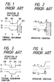
- Figs. 1 and 2 are band charts showing the function states of a PNM device
- Figs. 3 and 4 are band charts showing the function states of a PNP device, wherein shown are an emitter 201, 210; a base 202, 211; a collector 203, 212; and a depletion layer 204, 213 between the collector and the base.
- the movement of the positive holes, functioning as the principal carriers, is same in both devices.
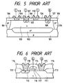
- FIG. 5 illustrates a conventional PNM semiconductor device, wherein shown are semiconductor substrate 101 for example of p-type; an n+ buried layer 102 constituting the collector; an n-epitaxial layer 103 constituting the actual device; an isolation area 104; a diffused emitter area 105; emitter and base electrodes 107; Shottky electrodes 108 composed for example of aluminum for constituting Shottky junctions with the epitaxial layer 103; an insulation layer 106 composed for example of SiO2 for insulating the emitter, base electrodes 107 and the metal layers 108 from the semiconductor surface; and a diffusion layer 109 for electrical connection with the base electrode 107.
- Fig. 6 shows a conventional structure in which a Shottky junction is utilized in the drain portion, wherein shown are an n-type semiconductor substrate 111; a diffusion layer 112 constituting a source area; an isolation oxide film 113 formed for example by LOCOS (local oxidation of silicon); an insulation layer 114 composed for example of phosphor glass; a Shottky electrode 115 composed for example of Al; a gate oxide film 116; a gate electrode 117; and a source electrode 118.
- LOCOS local oxidation of silicon
- the conventional PNM semiconductor device shown in Fig. 5 has been associated with a drawback of an extremely low current collecting efficiency because of a planar structure of the Shottky junction.
- the depletion layer 119 generated at the Shottky junction (collector) is concentrated in the surface area of the device and is therefore unable to efficiency collect the carriers diffusing from the emitter, so that the carriers leak to the device isolation area, leading to a lowered current gain. It is also necessary to effect control on the silicon substrate so as to realize satisfactory interface characteristics.
- the depletion layer 119 generates a protruding portion 119a extending along the surface of the device, thus forming a generation/recombination (G-R) area and hindering the improvement in the device characteristics. It is also conceived, in order to prevent such drawback, to form a highly doped layer 120 in a position corresponding to said protruding portion 119a as shown in Fig. 9, but a significant improvement in the characteristics cannot be expected with such structure since the area of the depletion layer 119 is inevitably limited.
- a principal object of the present invention is to provide a semiconductor device capable of high-speed rectifying operation and a method for producing the same.
- Another object of the present invention is to provide a highly reliable semiconductor device of satisfactory performance and a sufficiently high breakdown voltage with a low cost.
- Still another object of the present invention is to provide a semiconductor device having a metal electrode constituting a Shottky junction, formed by a CVD process utilizing alkylaluminum hydride and hydrogen.
- Still another object of the present invention is to provide a semiconductor device having a Shottky junction consisting of a monocrystalline metal and a semiconductor area.
- Still another object of the present invention is to provide a semiconductor device in which a Shottky junction is formed by burying metal in a recess formed in a semiconductor area.
- a semiconductor device having a Shottky junction consisting of a metal electrode and a semiconductor area, wherein said metal electrode is formed by a single crystal principally composed of Al.
- a method for producing a semiconductor device in which a Shottky electrode area is formed by a chemical vapor deposition (CVD) process utilizing alkylaluminum hydride gas and hydrogen.
- CVD chemical vapor deposition
- the present invention enables the preparation of a Shottky barrier diode in well controlled and uniform manner by controlling the reaction between Al and Si, by selectively burying monocrystalline aluminum in a constant hole, utilizing the CVD process utilizing alkylaluminum hydride and hydrogen, called Al-CVD process.
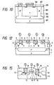
- Fig. 10 illustrates a semiconductor device having a Shottky junction embodying the present invention, provided with: a first semiconductor area of an n-type semiconductor; a second semiconductor area of an n-type semiconductor of a high resistance than in said first semiconductor area; an insulation film provided adjacent to said second semiconductor area and having an aperture; an electrode area formed in the area of said aperture; and a third semiconductor area of a p-type semiconductor formed at the junction of said insulation film and said electrode area; wherein said electrode area is composed of monocrystalline aluminum constituting a Shottky junction with said second semiconductor area.
- Fig. 10 illustrates, as an example of the semiconductor device having Shottky junction, a Shottky barrier diode.
- a p-type semiconductor substrate 301 On a p-type semiconductor substrate 301 there is formed a buried layer 302, on which an n-type layer 303 is epitaxially grown. From the principal surface of the substrate there is formed an n+ layer 304 for contacting with the buried layer 302, and said n+ layer is in ohmic contact with an upper cathode electrode.
- n layer 303 On the n layer 303 there are provided silicon oxide layers 305, 307, in which an aperture is formed to locally expose the n layer 303 and monocrystalline Al is formed therein to constitute a Shottky junction with said n layer 303.
- a p+-layer 306 is formed below and across the boundary between the anode electrode consisting of said monocrystalline Al and the silicon oxide insulation layer 305.
- the anode electrode in contact with the n-layer 303 including the junction thereof with the p+-layer 306 is formed by monocrystalline aluminum, the interface characteristics are improved to provide a satisfactory Shottky junction.
- Figs. 11A to 11D for explaining the method for producing the Shottky barrier diode of the present invention utilizing aluminum film.
- a semiconductor substrate 301 there is formed an n+-layer 302 of a high impurity concentration, as a buried layer for reducing the serial resistance (Fig. 11A).
- an n-semiconductor layer 303 is epitaxially grown.
- the impurity concentration is such as to form a Shottky junction with aluminum and is preferably 5 x 10¹⁶/cm3 or lower.
- n+-layer 304 of a high impurity concentration is formed for reducing the serial resistance, and a thin thermal oxide film 305 of 300 - 500 ⁇ is formed in the device forming area.
- a p+-layer 306 is formed thereon by ion implantation in order to secure the inverse voltage resistance of the Shottky barrier diode, and an interlayer insulation film 307 of a thickness of 3000 - 8000 ⁇ is formed by a CVD process (Fig. 11B).
- contact holes are formed by opening the interlayer insulation film 307 and the thermal oxide film 305 in desired positions by an ordinary photolithographic process, and aluminum for forming wiring electrodes is selectively grown in said contact holes by a CVD process to be explained later.
- the aluminum film formation is conducted, in a reaction chamber evacuated to a pressure of 5 x 10 ⁇ 3 Torr or lower, by introduction of dimethylaluminum hydride (DMAH) with H2 as carrier gas, with a total pressure of 0.5 - 760 Torr, preferably 0.1 to 0.8 Torr with a DMAH partial pressure of 1 x 10 ⁇ 5 to 1.3 x 10 ⁇ 3 times of the total pressure and with a substrate temperature of 270 - 350°C.
- DMAH dimethylaluminum hydride
- the formed Al film 308 grows as a single crystal selectively in the contact hole, and can fill in the contact hole with flat top surface (Fig. 11C).
- an Al film of a thickness of 4000 - 12000 ⁇ is formed by sputtering with a substrate temperature of 100 - 500°C without breaking the vacuum condition, and is subsequently patterned by a photolithographic process to form wiring electrodes 309.
- a second embodiment of the present invention provide a semiconductor device having a Shottky junction, capable of forming a depletion layer of a desired shape without reducing the area thereof, thereby achieving a significant improvement in the performance.
- the semiconductor device of the second embodiment includes a structure in which the substrate is provided with a recess at a position where the Shottky junction is to be formed, and a part of a metal layer is positioned in said recess.
- the Shottky electrode penetrates to a predetermined depth in the epitaxial layer, so that the depletion layer reaches the deep part of said epitaxial layer.
- the carriers diffusing from the emitter can be efficiently captured and an improvement in gain can therefore be attained.
- a semiconductor substrate 1 a buried layer 2; a device isolation layer 3; a diffused portion 4 of the emitter; a diffusion layer 5 for ohmic contact with the base electrode 7; base and emitter electrodes 7; a Shottky electrode 8 constituting a collector; an insulation layer 6 composed for example of SiO2 for insulating the semiconductor substrate 1 from the electrodes 7, 8; and an epitaxial layer 9.
- the electrodes 7 are in contact with the surface of the smiconductor substrate 1, while the electrodes 8 penetrate in recesses 10 formed on the surface of the semiconductor substrate 1, and form Shottky junctions between the end faces and the epitaxial layer 9.
- Fig. 13 for explaining the function of the semiconductor device explained above.
- the Shottky electrodes 8 penetrate to a predetermined depth in the epitaxial layer 9, the depletion layer 20 reaches the deeper part of the epitaxial layer 9 as will be apparent from the comparison with the conventional device shown in Fig. 7, whereby the carriers diffusing from the emitter can be efficiently captured by the collector and an improvement in the gain can be attained.
- Figs. 14A to 14D illustrate an example of the method for producing the semiconductor device shown in Fig. 12.
- a semiconductor substrate 501 there are shown a semiconductor substrate 501; a buried layer 502 constituting a part of the base; an epitaxial layer 504 constituting a device forming layer; a device isolation layer 503; a surface protective film 505; a diffusion layer 506 forming a contact to the base; and a diffusion area 507 serving as an emitter.
- the diffusion layers 506, 507 constituting the base and the emitter are formed according to an ordinary method.
- contact holes 508 are fomred in the surface protective film 505 by a photolithographic process and an etching process (Fig.
- recesses 509 are formed again by a photolithographic process and an etching process. Said recesses 509 penetrates the surface protective film 505 and reach a depth d from the surface of the epitaxial layer 504. Finally base and emitter electrodes 511 and collector electrodes 512 are formed in the contact holes 508 and the recesses 509 (Fig. 14D).
- the collector electrodes 512 for forming Shottky barriers can be formed by the Al-CVD process mentioned above. More specifically, a substrate to be subjected to the Al film formation is placed in a loading chamber, of which atmosphere is replaced by hydrogen gas. An adjacent reaction chamber is evacuated to a pressure of ca. 1 x 10 ⁇ 8 Torr. Into said reaction chamber there are introduced dimethylaluminum hydride (Al(CH3)2H: DMAH) with hydrogen as carrier gas, through a first gas line, and hydrogen gas as reaction gas through a second gas line. DMAH and hydrogen gas react in the reaction chamber, and the reacted gas contacts the substrate in the loading chamber. Said substrate is heated to about 270°C generally by lamps, and aluminum is deposited onto the substrate surface in this state. The Al-CVD process causes selective aluminum deposition in the grooves present on the substrate surface, providing satisfactory Al deposited film.
- Al(CH3)2H: DMAH dimethylaluminum hydride
- DMAH dimethylaluminum hydr
- Fig. 15 illustrates an embodiment of the present invention applied to a field effect transistor wherein shown are an epitaxial layer 11 formed on a semiconductor substrate; a diffusion layer 12 constituting a source; a device isolation area 13 formed by LOCOS; an insulation layer 14 composed for example of phosphate glass; a drain electrode 15; a gate insulation film 16; a gate electrode 17; and a Shottky electrode 18 constituting a source.
- the drain electrode 15 is composed of a metal, such as aluminum, constituting a Shottky barrier, and partly penetrates into a recess 19 formed in the epitaxial layer 11. Also in the semiconductor device of the present embodiment, as in the case of Fig.
- the Shottky junction S is formed in the deep part of the epitaxial layer 11, so that the carriers diffusing from the source can be efficiently collected by the drain and an improvement in the gain can therefore be attained.
- the Shottky barrier may be formed other metals than aluminum, such as Pt, W, Mo, Ni, Ti, Mn or Ta.
- a structure shown in Fig. 16 provided with an epitaxial layer 21, an insulation layer 22 and a Shottky electrode 23 penetrating into a recess 26, there may be formed a high impurity concentration layer 25 around said electrode 23. Also in this case, a depletion layer 24 is formed, reaching the deep part of the epitaxial layer 21, thereby reducing the surfacial G-R area without a significant decrease in the carrier collecting area.
- the semiconductor devices of the second and third embodiments have the effect of significantly improving the probability of capturing the carriers, diffusing from the emitter, by the collector, thereby attaining an improvement in the current gain, as the Shottky electrode penetrates to a predetermined depth in the epitaxial layer and the depletion layer formed therearound reaches the deep part of said epitaxial layer.
- the Al-CVD process employed for forming the Shottky electrode provides particularly satisfactory interface characteristics, thus allowing to obtain a satisfactory Shottky junction, and facilitates the control of preparation of the device.
- Al-CVD process a method for forming a metal film composed solely or principally of aluminum, adapted for use in the present invention, said method being called Al-CVD process.
- This method is suitable for filling a fine and deep aperture with an aspect ratio of 1 or larger, such as a contact hole or a through hole, with a metal material, and is characterized by a splended selectivity.
- the metal film formed by this method is characterized by spectacular crystallinity, such as monocrystalline aluminum, and is almost free from carbon inclusion.
- Said metal film has excellent surface characteristics, with a resistivity as low as 0.7 to 3.4 ⁇ cm, a reflectance as high as 85 to 95 %, and a density of hillocks equal to 1 ⁇ m or larger in a range of 1 to 100 cm ⁇ 2.
- said method consists of forming a deposition film by a surface reaction, on an electron-donating substrate, utilizing alkylaluminum hydride gas and hydrogen gas.
- An aluminum film of particularly satisfactory quality can be deposited by employing mono-methylaluminum hydride (MMAH) or dimethylaluminum hydride (DMAH) as the raw material gas and hydrogen as the reaction gas, and heating the substrate surface in the presence of a mixture of these transistor.
- MMAH mono-methylaluminum hydride
- DMAH dimethylaluminum hydride
- the substrate surface is preferably heated, either by direct or indirect heating, to a temperature range at least equal to the decomposition temperature of alkylaluminum hydride but lower than 450°C, more preferably within a range from 260 - 440°C.
- the substrate may be heated to the above-mentioned temperature range either by indirect or direct heating, but an aluminum film of satisfactory quality can be obtained with a particularly high deposition speed if the substrate is maintained within the above-mentioned temperature range by direct heating.
- a satisfactory film can be obtained with a deposition speed of 3000 - 5000 ⁇ /min., which is higher than the deposition speed obtainable with resistance heating.
- Such direct heating in which the substrate is heated by direct energy transfer from heating means, is for example achieved by heating with lamps, such as halogen lamps or xenon lamps.
- the indirect heating can for example be achieved by resistance heating, utilizing a heat generating member provided in a substrate support member, provided for supporting the substrate for film formation in a film forming chamber.
- This method when applied to a substrate having both an electron donating surface area and an electron non-donating surface area, forms monocrystalline aluminum with a satisfactory selectivity, solely on the electron donating surface area.
- the electron donating material means a material in which free electrons are present or intentionally generated, and which has a surface capable of accelerating a chemical reaction by electron transfer with molecules of the raw material gas deposited onto said surface.
- Metals and semiconductors generally fall into this category. Also metals and semiconductors having a thin surfacial oxide film are included in the electron donating materials of the present invention, since a chemical reaction can be induced by electron transfer between the substrate and the raw material molecules deposited thereon.
- Examples of the electron donating material include III-V compound semiconductors of two-, three- or multi-element system obtained by combining element(s) of group III such as Ga, In, Al etc. with element(s) of group V such as P, As, N etc.; semiconductors such as mono-crystalline or amorphous silicon; and metals, alloys and silicides such as tungsten, molybdenum, tantalum, copper, titanium, aluminum, titanium-aluminum, titanium nitride, aluminum-silicon-copper, aluminum-palladium, tungsten silicide, titanium silicide, aluminum silicide, molybdenum silicide and tantalum silicide.
- III-V compound semiconductors of two-, three- or multi-element system obtained by combining element(s) of group III such as Ga, In, Al etc. with element(s) of group V such as P, As, N etc.
- semiconductors such as mono-crystalline or amorphous silicon
- example,of the electron non-donating material constituting a surface not inducing selective deposition of Al or Al-Si, include silicon oxide formed by thermal oxidation or by CVD; glass materials such as BSG, PSG and BPSG; oxide films; thermal nitride films; and a silicon nitride film formed by plasma CVD, low pressure CVD, or ECR-CVD.
- Said Al-CVD method can also deposit following metal films principally composed of aluminum, with satisfactory film quality.
- a conductive material for electrode formation such as Al-Si, Al-Ti, Al-Cu, Al-Si-Ti or Al-Si-Cu by employing a mixed gaseous atmosphere containing a suitable combination, in addition to alkylaluminum hydride gas and hydrogen,of: Si-containing gas such as SiH4, Si2H6, Si3H8, Si(CH3)4, SiCl4, SiH2CL2, SiHCl3 etc.; Ti-containing gas such as TiCl4, TiBr4, Ti(CH3)4 etc.; and Cu-containing gas such as copper bisacetylacetonate (Cu(C5H7O2)2), copper bispyvaloylmethanite (Cu(C11H19O2)2), copper bishexafluoroacetyl-acetonate (Cu(C5HF6O2)2 etc.
- Si-containing gas such as SiH4, Si2H6, Si3H8, Si(CH3)4, SiCl4, SiH2CL2, SiHCl3 etc.
- said Al-CVD method is capable of film formation with excellent selectivity and with satisfactory surface characteristics of the obtained film
- non-selective film forming method in the succeeding film deposition to obtain a metal film solely or principally composed of aluminum both on the selectively deposited aluminum film and on the SiO2 insulation film, thereby obtaining a metal film generally usable as wirings for the semiconductor devices.
- Such metal film can be obtained by the combinations of non-selectively deposited Al, Al-Si, Al-Ti, Al-Cu, Al-Si-Ti or Al-Si-Cu and selectively deposited Al, Al-Si, Al-Ti, Al-Cu, Al-Si-Ti or Al-Si-Cu.
- Said non-selective film deposition can be achieved for example by a CVD method other than the above-explained Al-CVD method, or by sputtering.
- the wirings may also be formed by forming a conductive film by CVD or sputtering, patteening said film to obtain a sub layer of a form of desired wirings, and selectively depositing aluminum or a metal principally composed of aluminum on said sub layer by the Al-CVD method.
- a metal may be deposited on an insulation film by the Al-CVD method.
- the insulation film is subjected to a surface modification to form a substantially electron-donating surface area.
- a pattern of desired wirings may be drawn with a beam, whereby the film is selectively deposited only on the electron-donating area obtained by said beam drawing, and the wirings can be obtained in self-aligned manner without the patterning operation.
Landscapes
- Electrodes Of Semiconductors (AREA)
- Bipolar Transistors (AREA)
- Junction Field-Effect Transistors (AREA)
Applications Claiming Priority (4)
| Application Number | Priority Date | Filing Date | Title |
|---|---|---|---|
| JP17006590 | 1990-06-29 | ||
| JP170065/90 | 1990-06-29 | ||
| JP240493/90 | 1990-09-10 | ||
| JP24049390 | 1990-09-10 |
Publications (3)
| Publication Number | Publication Date |
|---|---|
| EP0465151A2 true EP0465151A2 (fr) | 1992-01-08 |
| EP0465151A3 EP0465151A3 (en) | 1993-05-12 |
| EP0465151B1 EP0465151B1 (fr) | 1998-08-26 |
Family
ID=26493186
Family Applications (1)
| Application Number | Title | Priority Date | Filing Date |
|---|---|---|---|
| EP91305868A Expired - Lifetime EP0465151B1 (fr) | 1990-06-29 | 1991-06-28 | Méthode de production d'un dispositif semi-conducteur avec jonction Schottky |
Country Status (7)
| Country | Link |
|---|---|
| US (1) | US5438218A (fr) |
| EP (1) | EP0465151B1 (fr) |
| KR (1) | KR950007347B1 (fr) |
| CN (1) | CN1021943C (fr) |
| AT (1) | ATE170333T1 (fr) |
| DE (1) | DE69130041T2 (fr) |
| MY (1) | MY108622A (fr) |
Families Citing this family (12)
| Publication number | Priority date | Publication date | Assignee | Title |
|---|---|---|---|---|
| US5580808A (en) * | 1992-07-30 | 1996-12-03 | Canon Kabushiki Kaisha | Method of manufacturing a ROM device having contact holes treated with hydrogen atoms and energy beam |
| DE19737360C1 (de) * | 1997-08-27 | 1999-01-21 | Siemens Ag | Hochfrequenzdiode und Verfahren zu deren Herstellung |
| JP3273001B2 (ja) * | 1997-11-25 | 2002-04-08 | 株式会社東芝 | 半導体記憶装置とその製造方法 |
| US6455403B1 (en) * | 1999-01-04 | 2002-09-24 | Taiwan Semiconductor Manufacturing Company | Shallow trench contact structure to solve the problem of schottky diode leakage |
| JP4012040B2 (ja) * | 2002-10-31 | 2007-11-21 | キヤノン株式会社 | センタタップ終端回路及びセンタタップ終端回路を有するプリント配線板 |
| JP4089419B2 (ja) * | 2002-12-19 | 2008-05-28 | 株式会社村田製作所 | 半導体装置およびその製造方法 |
| JP4829476B2 (ja) * | 2004-03-09 | 2011-12-07 | オンセミコンダクター・トレーディング・リミテッド | ショットキーバリアダイオードおよびその製造方法 |
| FR2880193A1 (fr) * | 2004-12-23 | 2006-06-30 | St Microelectronics Sa | Diode schottky a barriere verticale |
| US8435873B2 (en) * | 2006-06-08 | 2013-05-07 | Texas Instruments Incorporated | Unguarded Schottky barrier diodes with dielectric underetch at silicide interface |
| EP2180517A1 (fr) * | 2008-10-24 | 2010-04-28 | Epcos Ag | Transistor bipolaire pnp avec un collecteur latéral et procédé de fabrication |
| US9929044B2 (en) * | 2014-01-30 | 2018-03-27 | Semiconductor Energy Laboratory Co., Ltd. | Method of manufacturing semiconductor device |
| JP6866326B2 (ja) * | 2018-03-19 | 2021-04-28 | 株式会社東芝 | 半導体装置 |
Family Cites Families (16)
| Publication number | Priority date | Publication date | Assignee | Title |
|---|---|---|---|---|
| JPS559428A (en) * | 1978-07-07 | 1980-01-23 | Internatl Rectifier Corp Japan Ltd | Method of manufacturing schottky barrier contact rectifier elements and schottky barrier contact rectifier element |
| JPS5766660A (en) * | 1980-10-09 | 1982-04-22 | Toshiba Corp | Semiconductor memory |
| US4665414A (en) * | 1982-07-23 | 1987-05-12 | American Telephone And Telegraph Company, At&T Bell Laboratories | Schottky-barrier MOS devices |
| JPS5992575A (ja) * | 1982-11-19 | 1984-05-28 | Hitachi Ltd | 半導体集積回路装置におけるシヨツトキバリアダイオ−ド |
| JPS6068661A (ja) * | 1983-09-26 | 1985-04-19 | Fujitsu Ltd | 半導体装置 |
| JPS60178670A (ja) * | 1984-02-24 | 1985-09-12 | Nec Corp | シヨツトキ−バリアダイオ−ド |
| JPS613470A (ja) * | 1984-06-18 | 1986-01-09 | Nec Corp | 半導体装置 |
| JPS62123716A (ja) * | 1985-11-22 | 1987-06-05 | Nec Corp | 半導体装置の製造方法 |
| GB2195663B (en) * | 1986-08-15 | 1990-08-22 | Nippon Telegraph & Telephone | Chemical vapour deposition method and apparatus therefor |
| JPS6394675A (ja) * | 1986-10-09 | 1988-04-25 | Fujitsu Ltd | 半導体装置 |
| JPS63114167A (ja) * | 1986-10-31 | 1988-05-19 | Toshiba Corp | 半導体装置の製造方法 |
| JPS63193571A (ja) * | 1987-02-05 | 1988-08-10 | Nec Corp | 縦形シヨツトキ電界効果トランジスタの形成方法 |
| JPS6423569A (en) * | 1987-07-20 | 1989-01-26 | Matsushita Electronics Corp | Schottky barrier semiconductor |
| US4952992A (en) * | 1987-08-18 | 1990-08-28 | Siliconix Incorporated | Method and apparatus for improving the on-voltage characteristics of a semiconductor device |
| JPH0251274A (ja) * | 1988-08-15 | 1990-02-21 | Nec Corp | ショットキダイオードの製造方法 |
| US5040034A (en) * | 1989-01-18 | 1991-08-13 | Nissan Motor Co., Ltd. | Semiconductor device |
-
1991
- 1991-06-28 EP EP91305868A patent/EP0465151B1/fr not_active Expired - Lifetime
- 1991-06-28 AT AT91305868T patent/ATE170333T1/de not_active IP Right Cessation
- 1991-06-28 DE DE69130041T patent/DE69130041T2/de not_active Expired - Fee Related
- 1991-06-29 MY MYPI91001180A patent/MY108622A/en unknown
- 1991-06-29 KR KR1019910011037A patent/KR950007347B1/ko not_active Expired - Fee Related
- 1991-06-29 CN CN91104304A patent/CN1021943C/zh not_active Expired - Fee Related
-
1993
- 1993-04-30 US US08/054,831 patent/US5438218A/en not_active Expired - Fee Related
Also Published As
| Publication number | Publication date |
|---|---|
| DE69130041D1 (de) | 1998-10-01 |
| ATE170333T1 (de) | 1998-09-15 |
| DE69130041T2 (de) | 1999-02-18 |
| EP0465151A3 (en) | 1993-05-12 |
| EP0465151B1 (fr) | 1998-08-26 |
| CN1058117A (zh) | 1992-01-22 |
| US5438218A (en) | 1995-08-01 |
| KR950007347B1 (ko) | 1995-07-10 |
| CN1021943C (zh) | 1993-08-25 |
| KR920001746A (ko) | 1992-01-30 |
| MY108622A (en) | 1996-10-31 |
Similar Documents
| Publication | Publication Date | Title |
|---|---|---|
| EP0460861B1 (fr) | Dispositif semiconducteur comportant une structure d'interconnection améliorée | |
| KR100362751B1 (ko) | 반도체소자의콘택트홀및그형성방법 | |
| US8901670B2 (en) | Semiconductor device including multiple metal semiconductor alloy region and a gate structure covered by a continuous encapsulating layer | |
| EP0459773A2 (fr) | Dispositif semi-conducteur et son procédé de fabrication | |
| US5438218A (en) | Semiconductor device with Shottky junction | |
| EP0068154A2 (fr) | Circuit intégré comportant un substrat semiconducteur ayant des régions d'isolation et des régions électriquement conductrices | |
| US4698127A (en) | Process for fabricating a self-aligned bipolar transistor | |
| US6218223B1 (en) | Process for producing electrode for semiconductor element and semiconductor device having the electrode | |
| US5663097A (en) | Method of fabricating a semiconductor device having an insulating side wall | |
| EP0475607B1 (fr) | Procédé de fabrication d'un dispositif semi-conducteur comprenant une diode à barrière Schottky | |
| US10347491B2 (en) | Forming recombination centers in a semiconductor device | |
| US5364802A (en) | Method of making a semiconductor device with buried electrode | |
| US5670417A (en) | Method for fabricating self-aligned semiconductor component | |
| EP0480580A2 (fr) | Pocédé pour la fabrication d'une structure d'électrode de dispositif à semi-conducteur | |
| JPH0845878A (ja) | 半導体装置の製造方法 | |
| US20240258424A1 (en) | Silicon carbide semiconductor device and method of manufacturing the same | |
| JP2010251368A (ja) | バイポーラトランジスタ及びその製造方法 | |
| EP4071786A1 (fr) | Procédé de formation d'un contact ohmique sur un semi-conducteur à bande large et dispositif à semi-conducteur à bande large | |
| JPH04355965A (ja) | ショットキー接合を有する半導体装置 | |
| US20250227980A1 (en) | Semiconductor device and manufacturing method thereof | |
| US12520552B2 (en) | Method of manufacturing a semiconductor device and semiconductor device | |
| US20250311289A1 (en) | Semiconductor device and manufacturing method therefor | |
| JPH0529248A (ja) | 半導体装置およびその製造方法 | |
| JP2786313B2 (ja) | 半導体装置およびその製造方法 | |
| JPH04304627A (ja) | 半導体装置及びその製造方法 |
Legal Events
| Date | Code | Title | Description |
|---|---|---|---|
| PUAI | Public reference made under article 153(3) epc to a published international application that has entered the european phase |
Free format text: ORIGINAL CODE: 0009012 |
|
| AK | Designated contracting states |
Kind code of ref document: A2 Designated state(s): AT BE CH DE DK ES FR GB GR IT LI LU NL SE |
|
| RTI1 | Title (correction) | ||
| PUAL | Search report despatched |
Free format text: ORIGINAL CODE: 0009013 |
|
| AK | Designated contracting states |
Kind code of ref document: A3 Designated state(s): AT BE CH DE DK ES FR GB GR IT LI LU NL SE |
|
| 16A | New documents despatched to applicant after publication of the search report | ||
| 17P | Request for examination filed |
Effective date: 19930924 |
|
| 17Q | First examination report despatched |
Effective date: 19951030 |
|
| GRAG | Despatch of communication of intention to grant |
Free format text: ORIGINAL CODE: EPIDOS AGRA |
|
| GRAG | Despatch of communication of intention to grant |
Free format text: ORIGINAL CODE: EPIDOS AGRA |
|
| GRAH | Despatch of communication of intention to grant a patent |
Free format text: ORIGINAL CODE: EPIDOS IGRA |
|
| GRAH | Despatch of communication of intention to grant a patent |
Free format text: ORIGINAL CODE: EPIDOS IGRA |
|
| RHK1 | Main classification (correction) |
Ipc: H01L 29/73 |
|
| GRAA | (expected) grant |
Free format text: ORIGINAL CODE: 0009210 |
|
| AK | Designated contracting states |
Kind code of ref document: B1 Designated state(s): AT BE CH DE DK ES FR GB GR IT LI LU NL SE |
|
| PG25 | Lapsed in a contracting state [announced via postgrant information from national office to epo] |
Ref country code: IT Free format text: LAPSE BECAUSE OF FAILURE TO SUBMIT A TRANSLATION OF THE DESCRIPTION OR TO PAY THE FEE WITHIN THE PRESCRIBED TIME-LIMIT;WARNING: LAPSES OF ITALIAN PATENTS WITH EFFECTIVE DATE BEFORE 2007 MAY HAVE OCCURRED AT ANY TIME BEFORE 2007. THE CORRECT EFFECTIVE DATE MAY BE DIFFERENT FROM THE ONE RECORDED. Effective date: 19980826 Ref country code: ES Free format text: THE PATENT HAS BEEN ANNULLED BY A DECISION OF A NATIONAL AUTHORITY Effective date: 19980826 Ref country code: BE Free format text: LAPSE BECAUSE OF FAILURE TO SUBMIT A TRANSLATION OF THE DESCRIPTION OR TO PAY THE FEE WITHIN THE PRESCRIBED TIME-LIMIT Effective date: 19980826 Ref country code: CH Free format text: LAPSE BECAUSE OF FAILURE TO SUBMIT A TRANSLATION OF THE DESCRIPTION OR TO PAY THE FEE WITHIN THE PRESCRIBED TIME-LIMIT Effective date: 19980826 Ref country code: GR Free format text: LAPSE BECAUSE OF NON-PAYMENT OF DUE FEES Effective date: 19980826 Ref country code: AT Free format text: LAPSE BECAUSE OF FAILURE TO SUBMIT A TRANSLATION OF THE DESCRIPTION OR TO PAY THE FEE WITHIN THE PRESCRIBED TIME-LIMIT Effective date: 19980826 Ref country code: LI Free format text: LAPSE BECAUSE OF FAILURE TO SUBMIT A TRANSLATION OF THE DESCRIPTION OR TO PAY THE FEE WITHIN THE PRESCRIBED TIME-LIMIT Effective date: 19980826 Ref country code: NL Free format text: LAPSE BECAUSE OF FAILURE TO SUBMIT A TRANSLATION OF THE DESCRIPTION OR TO PAY THE FEE WITHIN THE PRESCRIBED TIME-LIMIT Effective date: 19980826 |
|
| REF | Corresponds to: |
Ref document number: 170333 Country of ref document: AT Date of ref document: 19980915 Kind code of ref document: T |
|
| REG | Reference to a national code |
Ref country code: CH Ref legal event code: EP |
|
| REF | Corresponds to: |
Ref document number: 69130041 Country of ref document: DE Date of ref document: 19981001 |
|
| PG25 | Lapsed in a contracting state [announced via postgrant information from national office to epo] |
Ref country code: SE Free format text: LAPSE BECAUSE OF FAILURE TO SUBMIT A TRANSLATION OF THE DESCRIPTION OR TO PAY THE FEE WITHIN THE PRESCRIBED TIME-LIMIT Effective date: 19981126 Ref country code: DK Free format text: LAPSE BECAUSE OF FAILURE TO SUBMIT A TRANSLATION OF THE DESCRIPTION OR TO PAY THE FEE WITHIN THE PRESCRIBED TIME-LIMIT Effective date: 19981126 |
|
| ET | Fr: translation filed | ||
| NLV1 | Nl: lapsed or annulled due to failure to fulfill the requirements of art. 29p and 29m of the patents act | ||
| REG | Reference to a national code |
Ref country code: CH Ref legal event code: PL |
|
| PG25 | Lapsed in a contracting state [announced via postgrant information from national office to epo] |
Ref country code: LU Free format text: LAPSE BECAUSE OF NON-PAYMENT OF DUE FEES Effective date: 19990628 |
|
| PLBE | No opposition filed within time limit |
Free format text: ORIGINAL CODE: 0009261 |
|
| STAA | Information on the status of an ep patent application or granted ep patent |
Free format text: STATUS: NO OPPOSITION FILED WITHIN TIME LIMIT |
|
| 26N | No opposition filed | ||
| REG | Reference to a national code |
Ref country code: GB Ref legal event code: IF02 |
|
| PGFP | Annual fee paid to national office [announced via postgrant information from national office to epo] |
Ref country code: GB Payment date: 20060616 Year of fee payment: 16 |
|
| PGFP | Annual fee paid to national office [announced via postgrant information from national office to epo] |
Ref country code: FR Payment date: 20060629 Year of fee payment: 16 |
|
| PGFP | Annual fee paid to national office [announced via postgrant information from national office to epo] |
Ref country code: DE Payment date: 20060824 Year of fee payment: 16 |
|
| GBPC | Gb: european patent ceased through non-payment of renewal fee |
Effective date: 20070628 |
|
| REG | Reference to a national code |
Ref country code: FR Ref legal event code: ST Effective date: 20080229 |
|
| PG25 | Lapsed in a contracting state [announced via postgrant information from national office to epo] |
Ref country code: DE Free format text: LAPSE BECAUSE OF NON-PAYMENT OF DUE FEES Effective date: 20080101 |
|
| PG25 | Lapsed in a contracting state [announced via postgrant information from national office to epo] |
Ref country code: GB Free format text: LAPSE BECAUSE OF NON-PAYMENT OF DUE FEES Effective date: 20070628 |
|
| PG25 | Lapsed in a contracting state [announced via postgrant information from national office to epo] |
Ref country code: FR Free format text: LAPSE BECAUSE OF NON-PAYMENT OF DUE FEES Effective date: 20070702 |