EP0466975B1 - Dispositif semiconducteur émetteur de lumière - Google Patents
Dispositif semiconducteur émetteur de lumière Download PDFInfo
- Publication number
- EP0466975B1 EP0466975B1 EP90124199A EP90124199A EP0466975B1 EP 0466975 B1 EP0466975 B1 EP 0466975B1 EP 90124199 A EP90124199 A EP 90124199A EP 90124199 A EP90124199 A EP 90124199A EP 0466975 B1 EP0466975 B1 EP 0466975B1
- Authority
- EP
- European Patent Office
- Prior art keywords
- light
- semiconductor light
- resin
- emitting element
- emitting
- Prior art date
- Legal status (The legal status is an assumption and is not a legal conclusion. Google has not performed a legal analysis and makes no representation as to the accuracy of the status listed.)
- Expired - Lifetime
Links
Images
Classifications
-
- H—ELECTRICITY
- H10—SEMICONDUCTOR DEVICES; ELECTRIC SOLID-STATE DEVICES NOT OTHERWISE PROVIDED FOR
- H10H—INORGANIC LIGHT-EMITTING SEMICONDUCTOR DEVICES HAVING POTENTIAL BARRIERS
- H10H20/00—Individual inorganic light-emitting semiconductor devices having potential barriers, e.g. light-emitting diodes [LED]
- H10H20/80—Constructional details
- H10H20/85—Packages
- H10H20/852—Encapsulations
- H10H20/853—Encapsulations characterised by their shape
-
- G—PHYSICS
- G02—OPTICS
- G02B—OPTICAL ELEMENTS, SYSTEMS OR APPARATUS
- G02B6/00—Light guides; Structural details of arrangements comprising light guides and other optical elements, e.g. couplings
- G02B6/24—Coupling light guides
- G02B6/42—Coupling light guides with opto-electronic elements
- G02B6/4201—Packages, e.g. shape, construction, internal or external details
- G02B6/4204—Packages, e.g. shape, construction, internal or external details the coupling comprising intermediate optical elements, e.g. lenses, holograms
- G02B6/4212—Packages, e.g. shape, construction, internal or external details the coupling comprising intermediate optical elements, e.g. lenses, holograms the intermediate optical element being a coupling medium interposed therebetween, e.g. epoxy resin, refractive index matching material, index grease, matching liquid or gel
-
- H—ELECTRICITY
- H10—SEMICONDUCTOR DEVICES; ELECTRIC SOLID-STATE DEVICES NOT OTHERWISE PROVIDED FOR
- H10H—INORGANIC LIGHT-EMITTING SEMICONDUCTOR DEVICES HAVING POTENTIAL BARRIERS
- H10H20/00—Individual inorganic light-emitting semiconductor devices having potential barriers, e.g. light-emitting diodes [LED]
- H10H20/80—Constructional details
- H10H20/85—Packages
- H10H20/855—Optical field-shaping means, e.g. lenses
- H10H20/856—Reflecting means
Definitions
- This invention relates to a semiconductor light-emitting device which can be used in a light pickup of an optical disc apparatus, or as a module in an optical communications system, or the like, as ontlined in the preamble of claim 1.
- a conventional semiconductor light-emitting device comprises a semiconductor light-emitting element mounted on a heat sink block which, in turn, is mounted on a stem.
- the semiconductor light-emitting element, the heat sink block and the stem are covered by a hollow envelope joined to the stem. Light goes out through a glass window provided in the hollow envelope.
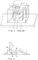
- a semiconductor light-emitting element 1 is mounted on a base 4 with an Si submount 2 and a heat sink block 3 interposed therebetween, and the element 1, the submount 2 and the heat sink block 3 are sealed in a transparent resin on the base 4.
- Light 6 emitted from the semiconductor light-emitting element 1 emerges through the transparent resin 5.
- the emitted light 6 from the semiconductor light-emitting element 1 of the semiconductor light-emitting device shown in Figure 1 is usually made to pass through one or more of optical elements, such as a beam splitter, a lens, an optical fiber, a glass plate and the like.
- the emitted light 6 must have an optically undistorted light intensity distribution so that coupling of light to an optical system is not adversely affected. If the light intensity distribution is distorted, it is difficult to obtain for example, a parallel light beam.
- the emitted light 6 emerges from the device through a surface portion 7 of the transparent resin, and, therefore, the flatness of the surface portion 7 which interfaces with exterior is critical.
- the portion 7 does not have an optically desirable surface state, the light intensity distribution of the emitted light 6 is distorted and, therefore, undesired optical coupling with a succeeding optical system may result.
- the portion 7 could be finished by, for example, polishing.
- polishing it is difficult to provide such working as to give flatness of the same degree as those of optical elements to the surface portion 7, and the productivity of such finishing is low.
- a surface of such resins is not suitable for use as a light emerging surface.
- a semiconductor light-emitting device as outlined in claim 1 is provided.
- a semiconductor light-emitting device includes a semiconductor light-emitting element and a beam splitter or a glass plate disposed in such a predetermined position that light emitted by the semiconductor light-emitting element travels through said elements.
- the light-emitting element and part of said optical element are sealed in a transparent resin member comprising a resin which is transparent to the light emitted by the semiconductor light-emitting element, in such a manner that the entire optical path extruding between the semiconductor light-emitting element and the light entrance portion of said optical element is positioned within the resin member.
- the light exit portion of said optical element from which the light emitted by the semiconductor light-emitting element exits the device is positioned outside of the resin member.
- At least one additional optical element can be disposed in the optical path between the semiconductor light-emitting element and the light entrance portion of the cited optical element.
- the resin member isolates the semiconductor light-emitting element from the external atmosphere and also secures the light-emitting element and the optical element in a predetermined positional relationship.
- FIG. 2 illustrates a semiconductor light-emitting device according to a prefered embodiment of the present invention.
- the semiconductor light-emitting device comprises a semiconductor light-emitting element 1 fixedly mounted on a base 4 and emitting light 6 from its light-emitting region 1a, and a beam splitter 8 also fixed to the base 4.
- a transparent resin 5 covers the entirety of the light-emitting element 1 on the base 4, and also a substantial portion of the beam splitter 8, including a light incident portion of a surface 8a thereof, while leaving a light exit surface 8b exposed, whereby the entirety of the optical path 6a for light from the semiconductor light-emitting element 1 extending between the element 1 and the beam splitter 8 is located in the resin 5.
- the resin 5 is transparent to light emitted by the semiconductor light-emitting element 1.
- a cyclic aliphatic epoxy resin for example, may be used.
- Another resin such as diglycidyl ester, may also be usable.
- the transparent resin 5 adheres to and fills the space between the light-emitting region 1a of the light-emitting element 1 and the light incident surface 8a of the beam splitter 8, leaving no gap between the resin 5 and the region 1a or between the resin and the light entrance portion of the surface 8a.
- the light 6 emitted by the semiconductor light-emitting element 1 passes through the transparent resin 5, enters into the beam splitter 8 where it is deflected 90°, and emerges from the device from the surface 8b of the beam splitter 8. Since the beam splitter 8 has its light-incident surface 8a well-finished so as to give no distortion to light intensity distribution and, furthermore, it is in intimately contact with the resin, the light 6 emitted from the semiconductor light-emitting element 1 can emerge from the device without being distorted.
- optical elements for example, glass plates, other than the ones used in the described embodiment may be used.
- the optical elements usable in the present invention are light transmissive. Types, numbers and arrangements of optical elements in the sealing resin are determined in accordance with the purpose of the light-emitting device.
- the surface of sealing resin need not be provided with any special finishing as is provided for optical elements in order to produce undistorted, stable light output from a semiconductor light-emitting device because light emerges from the device through a well-finished surface of an optical element. Furthermore, because the light-emitting element is sealed in a resin, its stability against environment is improved, and also, the positional relationship between the light-emitting element and the associated optical element(s) can be maintained fixed.
Landscapes
- Physics & Mathematics (AREA)
- General Physics & Mathematics (AREA)
- Optics & Photonics (AREA)
- Led Device Packages (AREA)
- Optical Couplings Of Light Guides (AREA)
- Semiconductor Lasers (AREA)
Claims (4)
- Un dispositif émetteur de lumière à semiconducteurs comprenant :
un élément émetteur de lumière à semiconducteurs (1);
un élément optique (8) placé dans une relation de position prédéterminée par rapport à l'élément émetteur de lumière (1), de façon que la lumière (6) qui est émise par l'élément émetteur de lumière (1) se propage à travers cet élément optique (8) et
une résine (5) encapsulant et maintenant l'élément émetteur de lumière à semiconducteurs (1) et l'élément optique (8) dans la relation de position prédéterminée, cette résine étant transparente pour la lumière (6) qui est émise par l'élément émetteur de lumière (1),
caractérisé en ce que l'élément optique (8) est un diviseur de faisceau ou une lame de verre, la surface d'entrée de faisceau (8a) de cet élément optique (8) étant en contact avec la résine (5), la surface de sortie de faisceau (8b) de l'élément optique (8) n'étant pas recouverte par la résine, et la totalité du chemin optique pour la lumière émise par l'élément émetteur de lumière, s'étendant depuis l'élément émetteur de lumière jusqu'à la surface d'entrée de faisceau (8a) de l'élément optique, se trouve à l'intérieur de la résine (5). - Un dispositif émetteur de lumière à semiconducteurs selon la revendication 1,
caractérisé en ce qu'au moins un élément optique supplémentaire est placé entre la surface de sortie de faisceau (1a) de l'élément émetteur de lumière à semiconducteurs (1) et la surface d'entrée de faisceau (8a) de l'élément optique (8). - Un dispositif émetteur de lumière à semiconducteurs selon la revendication 1 ou 2,
caractérisé en ce que la résine (5) est une résine époxy aliphatique/cyclique. - Un dispositif émetteur de lumière à semiconducteurs selon la revendication 1 ou 2,
caractérisé en ce que la résine (5) consiste en un ester diglycidylique.
Applications Claiming Priority (2)
| Application Number | Priority Date | Filing Date | Title |
|---|---|---|---|
| JP2189917A JP2792722B2 (ja) | 1990-07-16 | 1990-07-16 | 半導体発光装置 |
| JP189917/90 | 1990-07-16 |
Publications (2)
| Publication Number | Publication Date |
|---|---|
| EP0466975A1 EP0466975A1 (fr) | 1992-01-22 |
| EP0466975B1 true EP0466975B1 (fr) | 1993-05-05 |
Family
ID=16249375
Family Applications (1)
| Application Number | Title | Priority Date | Filing Date |
|---|---|---|---|
| EP90124199A Expired - Lifetime EP0466975B1 (fr) | 1990-07-16 | 1990-12-14 | Dispositif semiconducteur émetteur de lumière |
Country Status (5)
| Country | Link |
|---|---|
| US (1) | US5105237A (fr) |
| EP (1) | EP0466975B1 (fr) |
| JP (1) | JP2792722B2 (fr) |
| KR (1) | KR950000112B1 (fr) |
| DE (1) | DE69001548T2 (fr) |
Families Citing this family (18)
| Publication number | Priority date | Publication date | Assignee | Title |
|---|---|---|---|---|
| US5444726A (en) * | 1990-11-07 | 1995-08-22 | Fuji Electric Co., Ltd. | Semiconductor laser device |
| US5590144A (en) * | 1990-11-07 | 1996-12-31 | Fuji Electric Co., Ltd. | Semiconductor laser device |
| TW253996B (fr) * | 1992-04-07 | 1995-08-11 | Fuji Electric Co Ltd | |
| US5367530A (en) * | 1992-05-29 | 1994-11-22 | Sanyo Electric Co., Ltd. | Semiconductor laser apparatus |
| JP2565279B2 (ja) * | 1992-09-25 | 1996-12-18 | 日本電気株式会社 | 光結合構造 |
| US5414293A (en) * | 1992-10-14 | 1995-05-09 | International Business Machines Corporation | Encapsulated light emitting diodes |
| EP0592746B1 (fr) * | 1992-10-14 | 1997-03-19 | International Business Machines Corporation | Diode électroluminescente encapsulée et méthode d'encapsulation |
| US5516727A (en) * | 1993-04-19 | 1996-05-14 | International Business Machines Corporation | Method for encapsulating light emitting diodes |
| JPH09307144A (ja) * | 1996-05-14 | 1997-11-28 | Matsushita Electric Ind Co Ltd | 発光素子及びその製造方法 |
| DE19714170C1 (de) * | 1997-03-21 | 1998-07-30 | Siemens Ag | Elektrooptisches Modul |
| JP2001021775A (ja) | 1999-07-09 | 2001-01-26 | Sumitomo Electric Ind Ltd | 光学装置 |
| US20030151832A1 (en) * | 2002-01-14 | 2003-08-14 | Arthur Berman | Method and apparatus for enclosing optical assemblies |
| US6999237B2 (en) * | 2001-09-12 | 2006-02-14 | Lightmaster Systems, Inc. | Method and apparatus for configuration and assembly of a video projection light management system |
| DE50111658D1 (de) * | 2001-09-14 | 2007-01-25 | Finisar Corp | Sende- und/oder empfangsanordnung zur optischen signalübertragung |
| EP1491927B1 (fr) | 2002-04-01 | 2013-02-27 | Ibiden Co., Ltd. | Substrat support de puce a circuit integre, et procede de fabrication de substrat support de puce a circuit integre. |
| JPWO2005052666A1 (ja) * | 2003-11-27 | 2008-03-06 | イビデン株式会社 | Icチップ実装用基板、マザーボード用基板、光通信用デバイス、icチップ実装用基板の製造方法、および、マザーボード用基板の製造方法 |
| JP2008032522A (ja) * | 2006-07-28 | 2008-02-14 | Nitta Ind Corp | 光ファイバを用いた触覚センサ |
| WO2016164035A1 (fr) | 2015-04-10 | 2016-10-13 | Hewlett Packard Enterprise Development Lp | Filtres surmoulés |
Family Cites Families (14)
| Publication number | Priority date | Publication date | Assignee | Title |
|---|---|---|---|---|
| DE226431C (fr) * | ||||
| JPS5333436A (en) * | 1976-09-09 | 1978-03-29 | Toshiba Corp | Alloy for high frequency induction heating vessel |
| US4478588A (en) * | 1978-03-06 | 1984-10-23 | Amp Incorporated | Light emitting diode assembly |
| JPS54127691A (en) * | 1978-03-28 | 1979-10-03 | Toshiba Corp | Semiconductor light emission device |
| JPS5545236U (fr) * | 1978-09-16 | 1980-03-25 | ||
| DE2913262C2 (de) * | 1979-04-03 | 1982-04-29 | Kabelwerke Reinshagen Gmbh, 5600 Wuppertal | Elektro-optische Verbindungsvorrichtung |
| JPS566038U (fr) * | 1979-06-25 | 1981-01-20 | ||
| DE3016103A1 (de) * | 1980-04-25 | 1981-10-29 | Siemens AG, 1000 Berlin und 8000 München | Verfahren zur herstellung transparenter geissharze |
| JPS5850572A (ja) * | 1981-09-22 | 1983-03-25 | 株式会社東芝 | デイスプレイ装置の製造方法 |
| EP0114258A1 (fr) * | 1982-11-30 | 1984-08-01 | Kabushiki Kaisha Toshiba | Capsulation en résine de dispositifs photovoltaiques à semi-conducteur |
| JPH084155B2 (ja) * | 1986-06-25 | 1996-01-17 | 松下電器産業株式会社 | 光コネクタモジユ−ル |
| JPS6314489A (ja) * | 1986-07-04 | 1988-01-21 | Mitsubishi Electric Corp | 半導体レ−ザ装置 |
| JPS6333877A (ja) * | 1986-07-29 | 1988-02-13 | Omron Tateisi Electronics Co | 光半導体装置 |
| JP2504533B2 (ja) * | 1988-09-02 | 1996-06-05 | 同和鉱業株式会社 | Led発光装置並びに該装置に用いる発光ブロックの製造方法 |
-
1990
- 1990-07-16 JP JP2189917A patent/JP2792722B2/ja not_active Expired - Lifetime
- 1990-12-14 DE DE9090124199T patent/DE69001548T2/de not_active Expired - Lifetime
- 1990-12-14 EP EP90124199A patent/EP0466975B1/fr not_active Expired - Lifetime
-
1991
- 1991-07-03 US US07/724,460 patent/US5105237A/en not_active Expired - Lifetime
- 1991-07-15 KR KR1019910012007A patent/KR950000112B1/ko not_active Expired - Fee Related
Also Published As
| Publication number | Publication date |
|---|---|
| JP2792722B2 (ja) | 1998-09-03 |
| KR950000112B1 (ko) | 1995-01-09 |
| DE69001548T2 (de) | 1993-09-09 |
| DE69001548D1 (de) | 1993-06-09 |
| KR920003566A (ko) | 1992-02-29 |
| US5105237A (en) | 1992-04-14 |
| JPH0474483A (ja) | 1992-03-09 |
| EP0466975A1 (fr) | 1992-01-22 |
Similar Documents
| Publication | Publication Date | Title |
|---|---|---|
| EP0466975B1 (fr) | Dispositif semiconducteur émetteur de lumière | |
| US4355323A (en) | Coupler comprising a light source and lens | |
| US4733094A (en) | Bidirectional optoelectronic component operating as an optical coupling device | |
| US5566265A (en) | Transmission and reception module for a bidirectional, optical message and signal transmission | |
| US8827572B2 (en) | Side coupling optical fiber assembly and fabrication method thereof | |
| US6932519B2 (en) | Optical device package | |
| EP0611975B1 (fr) | Sous-assemblage pour éléments optoélectroniques | |
| US7165896B2 (en) | Light transmitting modules with optical power monitoring | |
| US6786627B2 (en) | Light generating module | |
| EP0859255A2 (fr) | Structure de couplage optique avec résine gélifiée | |
| JP7117133B2 (ja) | 光サブアセンブリ及びその製造方法並びに光モジュール | |
| JP2002534813A (ja) | 光子装置の密閉封止方法と装置 | |
| JPH10321900A (ja) | 光モジュール | |
| US5255333A (en) | Opto-electronic transducer arrangement having a lens-type optical coupling | |
| KR100527160B1 (ko) | 양방향 광 모듈 팩키지 | |
| US20040258367A1 (en) | Electrooptical module | |
| JPH04333806A (ja) | 受光モジュール | |
| JPH10307237A (ja) | 一体型光通信用半導体装置 | |
| JPS60153184A (ja) | 受光素子 | |
| JP3295327B2 (ja) | 双方向光モジュール | |
| JPH06342114A (ja) | 気密光コネクタ | |
| US6808321B2 (en) | Optical communication module | |
| JPS5925284A (ja) | 光半導体装置 | |
| JP2902882B2 (ja) | 光コネクタ付半導体レーザ装置 | |
| JPH0521899A (ja) | 半導体レーザ装置 |
Legal Events
| Date | Code | Title | Description |
|---|---|---|---|
| PUAI | Public reference made under article 153(3) epc to a published international application that has entered the european phase |
Free format text: ORIGINAL CODE: 0009012 |
|
| 17P | Request for examination filed |
Effective date: 19901214 |
|
| AK | Designated contracting states |
Kind code of ref document: A1 Designated state(s): DE FR NL |
|
| 17Q | First examination report despatched |
Effective date: 19920311 |
|
| GRAA | (expected) grant |
Free format text: ORIGINAL CODE: 0009210 |
|
| AK | Designated contracting states |
Kind code of ref document: B1 Designated state(s): DE FR NL |
|
| REF | Corresponds to: |
Ref document number: 69001548 Country of ref document: DE Date of ref document: 19930609 |
|
| ET | Fr: translation filed | ||
| PLBE | No opposition filed within time limit |
Free format text: ORIGINAL CODE: 0009261 |
|
| STAA | Information on the status of an ep patent application or granted ep patent |
Free format text: STATUS: NO OPPOSITION FILED WITHIN TIME LIMIT |
|
| 26N | No opposition filed | ||
| REG | Reference to a national code |
Ref country code: FR Ref legal event code: D6 |
|
| PGFP | Annual fee paid to national office [announced via postgrant information from national office to epo] |
Ref country code: NL Payment date: 20091216 Year of fee payment: 20 |
|
| PGFP | Annual fee paid to national office [announced via postgrant information from national office to epo] |
Ref country code: FR Payment date: 20091221 Year of fee payment: 20 |
|
| PGFP | Annual fee paid to national office [announced via postgrant information from national office to epo] |
Ref country code: DE Payment date: 20091222 Year of fee payment: 20 |
|
| REG | Reference to a national code |
Ref country code: NL Ref legal event code: V4 Effective date: 20101214 |
|
| PG25 | Lapsed in a contracting state [announced via postgrant information from national office to epo] |
Ref country code: NL Free format text: LAPSE BECAUSE OF EXPIRATION OF PROTECTION Effective date: 20101214 |
|
| PG25 | Lapsed in a contracting state [announced via postgrant information from national office to epo] |
Ref country code: DE Free format text: LAPSE BECAUSE OF EXPIRATION OF PROTECTION Effective date: 20101214 |