EP0468502B1 - Déflecteur de lumière - Google Patents
Déflecteur de lumière Download PDFInfo
- Publication number
- EP0468502B1 EP0468502B1 EP91112514A EP91112514A EP0468502B1 EP 0468502 B1 EP0468502 B1 EP 0468502B1 EP 91112514 A EP91112514 A EP 91112514A EP 91112514 A EP91112514 A EP 91112514A EP 0468502 B1 EP0468502 B1 EP 0468502B1
- Authority
- EP
- European Patent Office
- Prior art keywords
- light
- aluminum oxide
- oxide film
- light deflector
- laser beam
- Prior art date
- Legal status (The legal status is an assumption and is not a legal conclusion. Google has not performed a legal analysis and makes no representation as to the accuracy of the status listed.)
- Expired - Lifetime
Links
- 239000010408 film Substances 0.000 claims description 79
- TWNQGVIAIRXVLR-UHFFFAOYSA-N oxo(oxoalumanyloxy)alumane Chemical compound O=[Al]O[Al]=O TWNQGVIAIRXVLR-UHFFFAOYSA-N 0.000 claims description 56
- 229910000838 Al alloy Inorganic materials 0.000 claims description 28
- 239000012788 optical film Substances 0.000 claims description 28
- 238000000034 method Methods 0.000 claims description 27
- 230000003287 optical effect Effects 0.000 claims description 23
- 238000007254 oxidation reaction Methods 0.000 claims description 15
- 230000003647 oxidation Effects 0.000 claims description 13
- 238000001704 evaporation Methods 0.000 claims description 8
- 230000008020 evaporation Effects 0.000 claims description 8
- 239000012535 impurity Substances 0.000 claims description 7
- 239000000463 material Substances 0.000 claims description 5
- 239000000126 substance Substances 0.000 claims description 4
- 238000005240 physical vapour deposition Methods 0.000 claims description 3
- 238000003980 solgel method Methods 0.000 claims description 3
- 238000005268 plasma chemical vapour deposition Methods 0.000 claims description 2
- 238000004544 sputter deposition Methods 0.000 claims description 2
- 238000002230 thermal chemical vapour deposition Methods 0.000 claims description 2
- 239000004065 semiconductor Substances 0.000 description 19
- XAGFODPZIPBFFR-UHFFFAOYSA-N aluminium Chemical compound [Al] XAGFODPZIPBFFR-UHFFFAOYSA-N 0.000 description 15
- 229910052782 aluminium Inorganic materials 0.000 description 13
- 239000000758 substrate Substances 0.000 description 12
- 239000010410 layer Substances 0.000 description 11
- 230000015572 biosynthetic process Effects 0.000 description 6
- 238000006243 chemical reaction Methods 0.000 description 6
- 238000009792 diffusion process Methods 0.000 description 5
- 239000007789 gas Substances 0.000 description 5
- 229910052751 metal Inorganic materials 0.000 description 5
- 239000002184 metal Substances 0.000 description 5
- 230000001681 protective effect Effects 0.000 description 4
- 239000002904 solvent Substances 0.000 description 4
- 239000000654 additive Substances 0.000 description 3
- 230000000996 additive effect Effects 0.000 description 3
- 239000013078 crystal Substances 0.000 description 3
- 230000000694 effects Effects 0.000 description 3
- 239000003792 electrolyte Substances 0.000 description 3
- 238000010894 electron beam technology Methods 0.000 description 3
- 239000007788 liquid Substances 0.000 description 3
- 239000002356 single layer Substances 0.000 description 3
- 238000007738 vacuum evaporation Methods 0.000 description 3
- NCGICGYLBXGBGN-UHFFFAOYSA-N 3-morpholin-4-yl-1-oxa-3-azonia-2-azanidacyclopent-3-en-5-imine;hydrochloride Chemical compound Cl.[N-]1OC(=N)C=[N+]1N1CCOCC1 NCGICGYLBXGBGN-UHFFFAOYSA-N 0.000 description 2
- QGZKDVFQNNGYKY-UHFFFAOYSA-N Ammonia Chemical compound N QGZKDVFQNNGYKY-UHFFFAOYSA-N 0.000 description 2
- XKRFYHLGVUSROY-UHFFFAOYSA-N Argon Chemical compound [Ar] XKRFYHLGVUSROY-UHFFFAOYSA-N 0.000 description 2
- IAUJSQSUSPMIEA-UHFFFAOYSA-N OB(O)O.OB(O)O.N.N.N Chemical compound OB(O)O.OB(O)O.N.N.N IAUJSQSUSPMIEA-UHFFFAOYSA-N 0.000 description 2
- PNEYBMLMFCGWSK-UHFFFAOYSA-N aluminium oxide Inorganic materials [O-2].[O-2].[O-2].[Al+3].[Al+3] PNEYBMLMFCGWSK-UHFFFAOYSA-N 0.000 description 2
- 238000012937 correction Methods 0.000 description 2
- 230000007797 corrosion Effects 0.000 description 2
- 238000005260 corrosion Methods 0.000 description 2
- 239000008367 deionised water Substances 0.000 description 2
- 229910021641 deionized water Inorganic materials 0.000 description 2
- 238000007598 dipping method Methods 0.000 description 2
- 238000011156 evaluation Methods 0.000 description 2
- 230000001105 regulatory effect Effects 0.000 description 2
- 239000000243 solution Substances 0.000 description 2
- 238000012546 transfer Methods 0.000 description 2
- JLTRXTDYQLMHGR-UHFFFAOYSA-N trimethylaluminium Chemical compound C[Al](C)C JLTRXTDYQLMHGR-UHFFFAOYSA-N 0.000 description 2
- XLYOFNOQVPJJNP-UHFFFAOYSA-N water Chemical compound O XLYOFNOQVPJJNP-UHFFFAOYSA-N 0.000 description 2
- VHUUQVKOLVNVRT-UHFFFAOYSA-N Ammonium hydroxide Chemical compound [NH4+].[OH-] VHUUQVKOLVNVRT-UHFFFAOYSA-N 0.000 description 1
- VVTSZOCINPYFDP-UHFFFAOYSA-N [O].[Ar] Chemical compound [O].[Ar] VVTSZOCINPYFDP-UHFFFAOYSA-N 0.000 description 1
- 230000005856 abnormality Effects 0.000 description 1
- 229910021529 ammonia Inorganic materials 0.000 description 1
- 235000011114 ammonium hydroxide Nutrition 0.000 description 1
- 239000010407 anodic oxide Substances 0.000 description 1
- 238000007743 anodising Methods 0.000 description 1
- 229910052786 argon Inorganic materials 0.000 description 1
- QVGXLLKOCUKJST-UHFFFAOYSA-N atomic oxygen Chemical compound [O] QVGXLLKOCUKJST-UHFFFAOYSA-N 0.000 description 1
- 238000005229 chemical vapour deposition Methods 0.000 description 1
- 229910052802 copper Inorganic materials 0.000 description 1
- 238000000151 deposition Methods 0.000 description 1
- 229910003460 diamond Inorganic materials 0.000 description 1
- 239000010432 diamond Substances 0.000 description 1
- 238000009826 distribution Methods 0.000 description 1
- 239000008151 electrolyte solution Substances 0.000 description 1
- 238000005516 engineering process Methods 0.000 description 1
- 239000011521 glass Substances 0.000 description 1
- 238000010438 heat treatment Methods 0.000 description 1
- 238000004519 manufacturing process Methods 0.000 description 1
- 238000005259 measurement Methods 0.000 description 1
- 239000000203 mixture Substances 0.000 description 1
- 239000001301 oxygen Substances 0.000 description 1
- 229910052760 oxygen Inorganic materials 0.000 description 1
- 230000002633 protecting effect Effects 0.000 description 1
- VXYADVIJALMOEQ-UHFFFAOYSA-K tris(lactato)aluminium Chemical compound CC(O)C(=O)O[Al](OC(=O)C(C)O)OC(=O)C(C)O VXYADVIJALMOEQ-UHFFFAOYSA-K 0.000 description 1
Images




Classifications
-
- G—PHYSICS
- G02—OPTICS
- G02B—OPTICAL ELEMENTS, SYSTEMS OR APPARATUS
- G02B5/00—Optical elements other than lenses
- G02B5/20—Filters
- G02B5/28—Interference filters
- G02B5/285—Interference filters comprising deposited thin solid films
- G02B5/286—Interference filters comprising deposited thin solid films having four or fewer layers, e.g. for achieving a colour effect
-
- G—PHYSICS
- G02—OPTICS
- G02B—OPTICAL ELEMENTS, SYSTEMS OR APPARATUS
- G02B5/00—Optical elements other than lenses
- G02B5/08—Mirrors
- G02B5/09—Multifaceted or polygonal mirrors, e.g. polygonal scanning mirrors; Fresnel mirrors
Definitions
- the present invention relates to a laser beam scanning optical device adapted for use in a laser beam printer, a copying machine utilizing image formation on a photosensitive member with a laser beam or the like, and more particularly to a light deflector for deflecting a laser beam from a light source and a method for forming such a light deflector.
- Such conventional laser beam scanning optical device generally employs a rotary polygon mirror as the light deflector for deflecting a light beam into scanning motion.
- a rotary polygon mirror is generally composed of an aluminum alloy, a plastic material or glass, with a reflection increasing film on the reflective faces for light deflection.
- remarkable progress in the mirror surface finishing technology in recent years has put the optical mirror finishing with diamond grinding into practice and has enabled to provide a rotary polygon mirror formed by direct mirror finishing of aluminum or aluminum alloys.
- the Japanese Laid-open Patent No. 58-184903 discloses a rotary polygon mirror formed by direct mirror finishing of aluminum or an aluminum alloy followed by formation of a transparent film by anodic oxidation on the finished mirror faces. Such anodized oxide film shows satisfactory adhesion to the underlying aluminum alloy, thus satisfactorily functioning as a protective film for the aluminum mirror face.
- the anodized aluminum oxide film disclosed in the above-mentioned Japanese Laid-open Patent No. 58-184903, is practically unusable, due to an excessively large variation in the reflection intensity depending on the incident angle, since the optical film thickness (nd) is designed as m ⁇ /2 ⁇ cos ⁇ (wherein m is a positive integer except zero, ⁇ is wavelength, and ⁇ is incident angle) and the reflected light intensity is designed to become maximum in a core of an incident angle at the center of the scanning range.
- the object of the present invention is to provide a light deflector composed principally of aluminum with reduced dependence on the incident angle.
- This object is achieved by a light deflector as claimed in claims 1 or 3, respectively.
- this object is achieved by a method for forming a light deflector as claimed in claims 6 or 12, respectively.
- the structures and methods according to claims 1, 3, 6 and 12 allow to form the aluminum oxide film with an optimum thickness in consideration of the refractive index of the aluminum substrate, wavelength and angle of the incident light, thereby minimizing the dependence on the incident angle.
- Fig. 1 is a plan view of a scanning optical device employing the rotary polygon mirror of the present invention, showing the function in a plane parallel to the deflection plane (a plane formed in time by the light beam deflected by the deflecting reflection face of the light deflector).
- a light beam emitted from a semiconductor laser 1 constituting the light source is converted into a substantially parallel beam by a collimating lens 2.
- a diaphragm 3 for defining the size of the light beam.
- the light beam transmitted by the diaphragm 3 enters a rotary polygon mirror 4, which is rotated at a high speed in a direction indicated by an arrow, whereby the incident light beam is deflected into a high-speed scanning motion.
- the deflected light beam is subjected to correction of f ⁇ characteristics by an f ⁇ lens 5, thereby being focused on a photosensitive member 6 constituting a scanned plane, and performing a linear scanning thereon.
- a corona charger for uniformly charging the surface of the photosensitive member, a developing unit for developing an electrostatic latent image formed on said photosensitive member into a visible toner image, and a transfer corona charger for transferring said toner image onto a recording sheet (all these components not shown), whereby information corresponding to the light beam generated by the semiconductor laser 1 is recorded on the recording sheet.
- the effective light beam scanning angle is defined as 2 ⁇ as shown in Fig. 1, and the angle between the light beam before entry into the rotary polygon mirror and the center of said effective deflection angle 2 ⁇ is defined as ⁇ .
- the incident angle ⁇ of the light beam to the reflecting face varies within a range of 9° - 56° by the rotation of the polygon mirror.
- the light from the semiconductor laser 1 is linearly polarized, and enters the polygon mirror in the S-polarized state. More specifically, the incident light beam to the deflecting reflection plane of the polygon mirror is S-polarized, namely polarized perpendicularly to the reflection section (plane including the incident light, reflected light and refracted light). Stated differently, the light entering the polygon mirror from the semiconductor laser is polarized perpendicularly to the deflecting plane.
- the polygon mirror 4 is principally composed of aluminum, with an aluminum oxide film on the deflecting reflection faces.
- r 0s being a real number
- r 1s being a complex number
- r 1s r 1s e i ⁇ 1s
- amplitude reflectance Fresnel coefficient
- intensity reflectance energy reflectance
- the rotary polygon mirror composed of aluminum alloy is used for example in an incident angle range of 9° - 56° as explained above, there is required a flat reflectance characteristic within said range.
- a flat S-component reflectance within the above angle range can be obtained at several optical film thicknesses, with the fluctuation of S-component reflectance within several per cent over a range of the optical film thickness of several tens of nanometers.
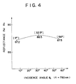
- a flat S-component reflectance over an incident angle range of 9° - 56° can be obtained at an optical film thickness (nd) of the anodized oxide film of 1240, 770, 596, 300 or 160 nm.
- the range of optical film thickness (nd) capable of maintaining the S-component reflectance within a fluctuation of 5 % is: 1215 - 1265 nm ( ⁇ /0.64 - ⁇ /0.61); 720 - 820 nm ( ⁇ /1.08 - ⁇ /0.95); 582 - 609 nm ( ⁇ /1.34 - ⁇ /1.28); 250 - 350 nm ( ⁇ /3,12 - ⁇ /2.23); or 142 - 180 nm ( ⁇ /5.5 - ⁇ /4.3).
- the ordinate indicates the S-component reflectance Rs while the abscissa indicates the incident angle ⁇ o .
- the rotary polygon mirror 4 is principally composed of aluminum, and the aluminum oxide film is formed on the deflecting reflection faces in the following manner.
- Fig. 5 illustrates the principle of anodic oxidation.
- rotary polygon mirrors 11 of an aluminum alloy are placed in an electrolytic tank 12 filled with electrolyte solution 13 (boric acid-ammonium borate buffer).
- electrolyte solution 13 boric acid-ammonium borate buffer
- an electrode which is connected to a DC power source 16.
- the aluminum oxide protective film is thus formed, and the thickness thereof can be precisely controlled by the current density between the electrodes and the time.
- the aluminum oxide layer could be simultaneously formed with a same thickness on all the deflecting reflections faces by a suitable arrangement of the electrodes.
- the oxidation reaction was conducted for example with a constant current of 4 mA/cm 2 and with a voltage up to 100 V, and the current was terminated when the optical film thickness of said aluminum oxide film reached 165 nm.
- Mg content 2.5 - 5.5 wt.%, more preferably 3.5 - 4.5 wt.%.
- Si is preferably not present as it is oxidized faster than Al, but the presence of a small amount is tolerated in consideration of the working ability.
- the Si content is preferably 0 - 0.5 wt.%, more preferably 0.05 wt.% or less.
- the total amount of other impurities is most preferably 0.001 wt.% or less.
- the electrolyte usable in the anodic oxidation is not limited to the boric acid-ammonium borate buffer explained above.
- a rotary mirror member obtained by mirror finishing of the aluminum alloy same as that used in the above-explained anodic oxidation, was cleaned with solvent, and mounted on a substrate holder with a rotating mechanism of a vacuum evaporation apparatus.
- Alumina crystals of ca. 2 cc was loaded as the evaporation source to be heated by electron beam, and the vacuum chamber was evacuated by a rotary oil pump and an oil diffusion pump.
- the pressure in the chamber reached 5 x 10 -4 Pa after about 15 minutes from the start of the oil diffusion pump, the rotary mirror member was heated to a surface temperature of about 150°C by a substrate heating device incorporated in the chamber.
- the electron beam heater was activated to melt the alumina crystal while the shutter of the evaporation source is closed, thereby eliminating wafer and gas contained in said crystals or present therearound.
- the substrate holder with a mechanism for rotating the substrate by itself and around the source, is put into motion whereby the mirror faces of the rotary mirror member face the evaporation source in succession.
- the dose of the electron beam was increased to obtain a evaporation rate of ca. 20 ⁇ /sec. and the shutter of the evaporation source was opened to form a thin aluminum oxide film on each mirror face of the rotary mirror member.
- a rotary mirror member obtained by mirror finishing of the aluminum alloy same as that used in the above-explained anodic oxidation, was cleaned with solvent, and mounted on a substrate holder of a vacuum reaction chamber.
- Said chamber was evacuated by a rotary oil pump and an oil diffusion pump.
- the pressure in said chamber reached 5 x 10 -4 Pa after about 15 minutes from the start of the oil diffusion pump, the rotary mirror member was heated to a surface temperature of ca. 300°C by a substrate heater incorporated in the reaction chamber.
- a gas valve connected thereto was suitably opened to introduce a 1:9 oxygen-argon mixture with a rate of 40 cc/min. Also another gas valve was opened to introduce gasified trimethylaluminum at a rate of 10 cc/min.
- a conductance value (evacuation regulating valve) positioned between the reaction chamber and the oil diffusion pump was suitably regulated to obtain a pressure of ca. 0.1 Pa in the reaction chamber, thereby depositing aluminum oxide on the rotary mirror member.
- the optical performance of thus prepared rotary mirror member of aluminum alloy was evaluated.
- the reflectance of the S-polarized light of a wavelength of 780 nm was almost constant within an incident angle range of 9° - 56°, with a fluctuation of 5 % or less.
- the incident angle dependence was little over a wide range of optical film thickness of 250 - 350 nm, there could be obtained rotary mirrors of stable performance.
- the aluminum oxide film can be obtained also by the CVD (plasma CVD or thermal CVD) method.
- a rotary mirror member obtained by mirror finishing of the aluminum alloy same as that used in the above-explained anodic oxidation, was cleaned with solvent, and mounted on a holder for chemical treatment. It was subsequently immersed in treating liquid containing 0.3 % of ammonia in deionized water.
- the treating liquid was maintained at 95° - 100°C and vigorously agitated, thereby forming aluminum oxide on the surface of the rotary mirror member.
- a dipping solution of basic aluminum lactate was placed in a tank and maintained at ca. 10°C.
- the substrates were then dried to a touch dry state for 30 minutes at 100°C and baked for 1 hour at 350°C.
- the reflectance of the S-polarized light with a wavelength of 780 nm was almost constant within an incident angle range of 9° - 56°, with fluctuation of 5 % or less. Besides, since the incident angle dependence was little over a wide range of optical film thickness of 582 - 609 nm, there could be obtained rotary mirrors of stable performance. In this manner the aluminum oxide film can also be obtained by the Sol-Gel method.
- the light deflector of the present invention principally composed of an aluminum alloy and used for light beam scanning, is provided, on the deflecting reflection faces thereof, with an aluminum oxide film of an optical film thickness (nd) of: ⁇ /5.5 - ⁇ /4.3; ⁇ /3,12 - ⁇ /2.23; ⁇ /1.34 - ⁇ /1.28; ⁇ /1.08 - ⁇ /0.95; or ⁇ /0.64 - ⁇ /0.61; wherein ⁇ is the wavelength of the scanning light.
- the incident light to said deflecting reflection faces is S-polarized, namely polarized perpendicularly to the reflection section (plane including the incident light, reflected light and refracted light).
- the above-explained light deflector of the present invention is capable of forming the aluminum oxide film with an optimum optical thickness, in consideration of the refractive index of aluminum substrate, and wavelength and angle of the incident light, thereby providing an advantage of minimizing the dependence on the incident angle.
- the present invention is capable of providing light deflector of stable performance, because the deflecting faces have satisfactory properties without film peeling, and also because the dependence on the incident angle is little over a wide range of optical film thickness.
- said film can achieve sufficient effect with a single layer, the time required for film formation can be reduced so that a significant economical effect can be obtained.
- the light deflector of the present invention principally composed of an aluminum alloy and used for light beam scanning, is preferably composed of an aluminum alloy with a Mg content within a range of 2.5 - 55 wt.%, a Si content within a range of 0 - 0.5 wt.%, and a content of other impurities not exceeding 0.001 wt.%.
- Such aluminum alloy with defined amounts of Mg and Si for maintaining desirable mirror finishing properties in the aluminum alloy, and with scarce contents of other impurities, provides the advantages of not causing abnormality in the surface properties of the reflection faces in the protective film forming step and in the preceding and succeeding steps, and also not causing undesirable effects on the protective film thus formed.
- the scanning optical device such as of a laser beam printer, generally employs a semiconductor laser as the light source. Because of its structure, the semiconductor laser emits a linearly polarized light beam, with a diverging angle different in the polarized direction and in the perpendicular direction. Also in the recording of image information by scanning a photosensitive member constituting the recording medium, as disclosed in the Japanese Patent Laid-open Application 52-119331, the image quality is improved by selecting the diameter of the light beam spot in the main scanning direction of the light deflector smaller than in the sub scanning direction (direction including the optical axis and perpendicular to the main scanning direction).
- the direction of larger diverging angle of the semiconductor laser (direction perpendicular to the junction plane of the laser) has been selected as the main scanning direction, in consideration of the foregoing conditions, as such selection can reduce the spot diameter and can improve the efficiency of utilization of the laser.
- the polarizing plane of the emitted light beam lies in the sub scanning direction, because of the nature of semiconductor laser.
- Such light beam enters the deflecting reflection planes of the light deflector in S-polarized state.
- Fig. 6 is a plan view of a scanning optical device employing the rotary polygon mirror of the present invention, showing the function in a main scanning plane parallel to the deflection plane (a plane formed in time by the light beam deflected by the deflecting reflection face of the light defector).
- a light beam emitted from a semiconductor laser 21 constituting the light source is converted into a substantially parallel beam by a collimating lens 2.
- a diaphragm 3 for defining the size of the light beam.
- the light beam transmitted by the diaphragm 3 enters, in the P-polarized state, the deflecting reflection plane of a light deflector consisting of a rotary polygon mirror 24, in such a manner that the polarizing direction is parallel to the main scanning plane.
- the incident light beam is P-polarized, namely the polarizing direction is parallel to the reflection plane (plane including the incident light, reflected light and refracted light).
- the light beam emitted by the semiconductor laser and entering the rotary polygon mirror is polarized in a direction parallel to the deflecting plane.
- the rotary polygon mirror 24 is rotated at a high speed, whereby the light beam entering the deflecting reflection plane is deflected at a high speed.
- the deflected light beam is subjected to the correction of f ⁇ characteristics by an f ⁇ lens 5 and is focused on a photosensitive member 6 constituting a scanned plane, thereby performing linear scanning.
- a corona charger for uniformly charging the surface of the photosensitive member, a developing unit for developing an electrostatic latent image formed on said photosensitive member into a visible toner image, and a transfer corona charger for transferring said toner image onto a recording sheet (all these components not shown), whereby information corresponding to the light beam generated by the semiconductor laser 21 is recorded on the recording sheet.
- the effective light beam scanning angle is defined as 2 ⁇ as shown in Fig. 6, and the angle between the light beam before entry into the rotary polygon mirror and the center of said effective deflection angle 2 ⁇ is defined as ⁇ .
- the incident angle ⁇ of the light beam to the reflecting face varies within a range of 10° - 55° by the rotation of the polygon mirror.
- the light from the semiconductor laser 21 is linearly polarized, and enters the deflecting reflection plane of the rotary polygon mirror in the P-polarized state. Consequently, as explained above, the narrower one of the diverging angles of the semiconductor laser 21 corresponds to the main scanning direction.
- the collimating lens 2 has an F number of 5.5 in the main scanning direction, with respect to the diaphragm 3.
- the rotary polygon mirror 24 is composed of aluminum, with an aluminum oxide film on the surface of mirror faces (reflection planes) thereof, with an optical film thickness of 108 nm.
- Fig. 7 shows the calculated incident angle dependence of the reflectance of the deflecting reflection face within an incident angle range of 10° - 55° in which said rotary polygon mirror is used.
- the incident angle dependence in the present embodiment is satisfactory, as small as ca. 0.3 %.
- the variation in the reflectance, resulting from the variation in the thickness of aluminum oxide film, is relatively small.
- Fig. 8 shows variation of the reflectance of the deflecting reflection face for the P-polarized light, generated by the variation in the film thickness at the maximum, center and minimum of the incident angle.
- Fig. 9 shows similar variation of the reflectance, generated by the variation in the film thickness, for the S-polarized light.
- the semiconductor laser When the semiconductor laser is used in the P-polarized state with respect to the deflecting reflection face of the light deflector, a narrower one of the light diverging angle (FFP angle) from the light emitting part of the semiconductor laser is used. If the light amount distribution varies on the diaphragm due to a fluctuation in said FFP angle, the spot diameter varies on the scanned plane. For this reason, in a FFP angle range of 7° - 20° in the main scanning direction (angular range where the light amount becomes 50 % of the maximum light amount), the F-number in the main scanning direction at the side of the semiconductor laser is selected at 4 or larger, thereby reducing the variation in the spot diameter in the main scanning direction on the scanned plane, by the FFP angle.
- FFP angle the light diverging angle
- the incident angle to the normal line to the deflecting reflection face is generally selected as a part within a range of 0° - 75°.
- the thickness of the Al 2 O 3 film is preferably 40 nm or larger, since the protecting effect of the film becomes weaker at a thickness less than 40 nm.
- the formation of aluminum oxide film on the aluminum surface is generally conducted by vacuum evaporation, but it is preferably achieved by anodic oxidation in the rotary polygon mirror of the present embodiment.
- the anodic oxidation is effective genenerally for formation of a film of 200 nm or less, when emphasis is given to the cost rather than the film forming time.
- the film formation by anodic oxidation may result in a shift or a gradation in the film thickness, due to locally uneven current density depending on the shape of the rotary polygon mirror or in case plural members are placed for mass production, but the present invention is also applicable in such case.
- ⁇ 90°
- ⁇ 54°
- wavelength ⁇ 780 nm
- incident angle range 18° - 72° to the deflecting reflection face.
- the rotary mirror was composed of aluminum, and Al 2 O 3 was deposited by evaporation, on the deflecting reflection faces, with an optical film thickness of 90 nm (0.115 ⁇ ).
- Fig. 10 shows the angle dependence of reflectance for the P-polarized light in this embodiment.
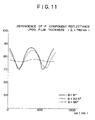
- Fig. 11 shows the change in reflectance R p of the deflecting reflection face for the P-polarized component, in ordinate, as a function of the optical film thickness (nd) of the anodic oxide film in abscissa.
- the range of optical film thickness (nd) in which the variation in reflectance of P-polarized component is within 5 % is 70 - 156 nm ( ⁇ /11.1 - ⁇ /5.0), 190 - 270 nm ( ⁇ /4.11 - ⁇ /2.89), 451 - 531 nm ( ⁇ /1.73 - ⁇ /1.47) or 609 - 650 nm ( ⁇ /1.28 - ⁇ /1.20).
- the range of optical film thickness (nd) in which the variation in reflectance of P-polarized component is within 3 % is: 83 - 110 nm ( ⁇ /9.4 - ⁇ /7.09), 216 - 243 nm ( ⁇ /3.61 - ⁇ /3.21) or 479 - 510 nm ( ⁇ /1.63 - ⁇ /1.53).
- rotary polygon mirrors have been explained as an example of light deflector, but the present invention is likewise applicable to a mirror with only one reflection face such as a Galvano mirror.
- the light deflector of the foregoing embodiment causes the linearly polarized light beam from the laser to enter the deflecting reflection face of the light deflector in the P-polarized state, and, when the light deflector is composed of aluminum with an aluminum oxide film on the reflection faces for increasing the reflectance, allows to suppress variation in the reflectance resulting from fluctuation in the thickness of said aluminum oxide film or resulting from variation in the incident angle, thereby enabling a precise scanning operation with uniform amount of light.
- the optical film thickness (nd) of aluminum oxide is 70 - 156 nm ( ⁇ /11.1 - ⁇ /5.0), 190 - 270 nm ( ⁇ /4.11 - ⁇ /2.89), 451 - 531 nm ( ⁇ /1.73 - ⁇ /1.47), or 609 - 650 nm ( ⁇ /1.28 - ⁇ /1.20).
- the linearly polarized light from the laser light source is made to enter said deflecting reflection faces in the S- or P-polarized state, thereby reducing the variation in reflectance resulting from fluctuation in the thickness of said aluminum oxide film or from the incident angle, thus achieving precise scanning operation on the scanned plane with a uniform amount of light.
Landscapes
- Physics & Mathematics (AREA)
- General Physics & Mathematics (AREA)
- Optics & Photonics (AREA)
- Mechanical Optical Scanning Systems (AREA)
- Laser Beam Printer (AREA)
- Optical Elements Other Than Lenses (AREA)
Claims (13)
- Déflecteur de lumière destiné à un dispositif optique de balayage de faisceau laser comprenant une source (1) de lumière qui émet un faisceau laser de longueur d'onde λ, ledit déflecteur de lumière comprenant :a) un élément (4) déflecteur de lumière constitué d'un matériau principalement composé d'un alliage d'aluminium ; etb) un film (22) d'oxyde d'aluminium formé sur une face réfléchissante de déflexion dudit élément (4) déflecteur de lumière, face sur laquelle le faisceau laser est incident,caractérisé en ce quec) l'épaisseur (nd) de film optique dudit film (22) d'oxyde d'aluminium se situe dans une gamme :
soit de λ/5,5 - λ/4,3;
soit de λ/3,12 - λ/2,23;
soit de λ/1,34 - λ/1,28;
soit de λ/0,64 - λ/0,61,
dans lequel la lumière dudit faisceau laser est à polarisation S. - Déflecteur de lumière selon la revendication 1,
caractérisé en ce que
ledit alliage d'aluminium constituant ledit élément (4) déflecteur de lumière a une teneur en Mg se situant dans une gamme de 2,5 - 5,5% en poids, une teneur en Si se situant dans une gamme de 0 - 0,5% en poids, et une teneur en autres impuretés ne dépassant pas 0,001% en poids. - Déflecteur de lumière destiné à un dispositif optique à balayage de faisceau laser comprenant une source (1) de lumière qui émet un faisceau laser de longueur d'onde λ, ledit déflecteur de lumière comprenant :a) un élément (4) déflecteur de lumière constitué d'un matériau principalement composé d'un alliage d'aluminium ; etb) un film (22) d'oxyde d'aluminium formé sur une face réfléchissante de déflexion dudit élément (4) déflecteur de lumière, face sur laquelle le faisceau laser est incident ;caractérisé en ce quec) l'épaisseur (nd) de film optique dudit film (22) d'oxyde d'aluminium se situe dans une gamme de:




- Dispositif optique à balayage comprenant une source (1) de lumière et un déflecteur de lumière selon l'une quelconque des revendications 1 à 3.
- Appareil d'enregistrement d'informations comprenant un élément (6) photosensible et des moyens (1-5) optiques agencés de façon à enregistrer des informations sur ledit élément photosensible, lesdits moyens à balayage optique comprenant une source (1) de lumière émettant un faisceau lumineux de longueur d'onde λ, et un déflecteur de lumière tel que défini dans l'une quelconque des revendications 1 à 3, ledit déflecteur de lumière étant positionné de façon que ledit élément (6) photosensible reçoive ledit faisceau lumineux dévié par ledit déflecteur de lumière.
- Procédé de formation d'un déflecteur de lumière destiné à un dispositif optique à balayage de faisceau laser comprenant une source (1) de lumière qui émet un faisceau laser de longueur d'onde λ, ledit procédé comprenant les étapes :a) d'utilisation d'un élément (4) déflecteur de lumière constitué d'un matériau principalement composé d'un alliage d'aluminium ; etb) de formation d'un film (22) d'oxyde d'aluminium sur une face réfléchissante de déflexion dudit élément (4) déflecteur de lumière, face sur laquelle le faisceau laser est incident,
caractérisé parc) la formation dudit film (22) d'oxyde d'aluminium avec une épaisseur (nd) de film optique qui se situe dans une gamme de :


- Procédé selon la revendication 6, caractérisé par la formation dudit film (22) d'oxyde d'aluminium par un procédé d'oxydation anodique.
- Procédé selon la revendication 6, caractérisé par la formation dudit film (22) d'oxyde d'aluminium par un procédé d'évaporation ou de pulvérisation (PVD).
- Procédé selon la revendication 6, caractérisé par la formation dudit film (22) d'oxyde d'aluminium par un procédé de dépôt chimique en phase vapeur (CVD) à plasma ou thermique.
- Procédé selon la revendication 6, caractérisé par la formation dudit film (22) d'oxyde d'aluminium par un procédé de traitement chimique.
- Procédé selon la revendication 6, caractérisé par la formation dudit film (22) d'oxyde d'aluminium par un procédé du type Sol-Gel.
- Procédé de formation d'un déflecteur de lumière destiné à un dispositif optique à balayage de faisceau laser comprenant une source (1) de lumière qui émet un faisceau laser de longueur d'onde λ, ledit procédé comprenant les étapes :a) de fourniture d'un élément (4) déflecteur de lumière constitué d'un matériau principalement composé d'un alliage d'aluminium ; etb) de formation d'un film (22) d'oxyde d'aluminium sur une face réfléchissante de déflexion dudit élément (4) déflecteur de lumière, face sur laquelle le faisceau laser est incident ;caractérisé parc) la formation dudit film (22) d'oxyde d'aluminium avec une épaisseur (nd) de film optique qui se situe dans une gamme de :




- Procédé selon la revendication 12, caractérisé par :
la formation dudit film (22) d'oxyde d'aluminium par un procédé d'oxydation anodique.
Applications Claiming Priority (6)
| Application Number | Priority Date | Filing Date | Title |
|---|---|---|---|
| JP199483/90 | 1990-07-26 | ||
| JP19948390A JP2810507B2 (ja) | 1990-07-26 | 1990-07-26 | 回転反射鏡 |
| JP2445991A JP3049662B2 (ja) | 1991-02-19 | 1991-02-19 | レーザー走査光学装置 |
| JP24459/91 | 1991-02-19 | ||
| JP19877591A JP2979754B2 (ja) | 1991-07-12 | 1991-07-12 | 光走査装置 |
| JP198775/91 | 1991-07-12 |
Publications (3)
| Publication Number | Publication Date |
|---|---|
| EP0468502A2 EP0468502A2 (fr) | 1992-01-29 |
| EP0468502A3 EP0468502A3 (en) | 1992-05-13 |
| EP0468502B1 true EP0468502B1 (fr) | 1997-03-05 |
Family
ID=27284659
Family Applications (1)
| Application Number | Title | Priority Date | Filing Date |
|---|---|---|---|
| EP91112514A Expired - Lifetime EP0468502B1 (fr) | 1990-07-26 | 1991-07-25 | Déflecteur de lumière |
Country Status (3)
| Country | Link |
|---|---|
| US (1) | US5604620A (fr) |
| EP (1) | EP0468502B1 (fr) |
| DE (1) | DE69124859T2 (fr) |
Families Citing this family (5)
| Publication number | Priority date | Publication date | Assignee | Title |
|---|---|---|---|---|
| EP0523677A3 (en) * | 1991-07-16 | 1994-10-19 | Canon Kk | Method and apparatus for anodic oxidation treatment |
| EP0550896A1 (fr) * | 1992-01-10 | 1993-07-14 | Eastman Kodak Company | Miroir optique avec réflectance uniforme |
| JP3507474B2 (ja) * | 2001-01-11 | 2004-03-15 | キヤノン株式会社 | 光走査装置及びそれを用いた画像形成装置 |
| US6847389B2 (en) * | 2003-05-02 | 2005-01-25 | Kabushiki Kaisha Toshiba | Optical beam scanning device and image forming apparatus |
| US20100181706A1 (en) * | 2005-07-13 | 2010-07-22 | Jari Ruuttu | Radiation Arrangement |
Family Cites Families (8)
| Publication number | Priority date | Publication date | Assignee | Title |
|---|---|---|---|---|
| JPS52119331A (en) * | 1976-03-31 | 1977-10-06 | Canon Inc | Laser recording device |
| JPS5546706A (en) * | 1978-09-29 | 1980-04-02 | Canon Inc | Phase difference reflecting mirror |
| JPS58184903A (ja) * | 1982-04-23 | 1983-10-28 | Hitachi Ltd | 回転反射鏡 |
| JPS59168411A (ja) * | 1983-03-16 | 1984-09-22 | Hitachi Ltd | 走査記録装置 |
| JPS59172624A (ja) * | 1983-03-23 | 1984-09-29 | Hitachi Ltd | 光偏向走査装置 |
| JPS6126765A (ja) * | 1984-07-13 | 1986-02-06 | Ricoh Co Ltd | 反射鏡の製造方法 |
| JP2653066B2 (ja) * | 1987-09-25 | 1997-09-10 | 富士ゼロックス株式会社 | 光ビーム偏向走査装置 |
| US5126873A (en) * | 1991-06-18 | 1992-06-30 | Xerox Corporation | Reflective surface coating for a uniform intensity of a polarized beam of a rotating polygon mirror optical scanning system |
-
1991
- 1991-07-25 EP EP91112514A patent/EP0468502B1/fr not_active Expired - Lifetime
- 1991-07-25 DE DE69124859T patent/DE69124859T2/de not_active Expired - Lifetime
-
1995
- 1995-06-07 US US08/474,969 patent/US5604620A/en not_active Expired - Lifetime
Also Published As
| Publication number | Publication date |
|---|---|
| EP0468502A2 (fr) | 1992-01-29 |
| DE69124859D1 (de) | 1997-04-10 |
| EP0468502A3 (en) | 1992-05-13 |
| US5604620A (en) | 1997-02-18 |
| DE69124859T2 (de) | 1997-07-03 |
Similar Documents
| Publication | Publication Date | Title |
|---|---|---|
| EP0468502B1 (fr) | Déflecteur de lumière | |
| US4753504A (en) | Mirror structure for laser printer | |
| JP3608504B2 (ja) | 赤外線レーザ用光学部品の製造方法 | |
| JP2810507B2 (ja) | 回転反射鏡 | |
| JPH10268107A (ja) | 反射防止膜付合成樹脂レンズ | |
| JPH0763903A (ja) | プラスチック製光学部品の光学薄膜およびその成膜方法 | |
| EP0161783B1 (fr) | Elément photorécepteur | |
| JP3689923B2 (ja) | 反射防止膜を有するプラスチックフィルムの製造方法 | |
| JPS61264350A (ja) | 電子写真感光体 | |
| JPS59109057A (ja) | 電子写真感光体 | |
| JP2956947B2 (ja) | 電子写真用感光体 | |
| JP2936743B2 (ja) | 電子写真感光体用基体およびその製造方法 | |
| JP3509414B2 (ja) | 反射鏡及びその製造方法 | |
| JPH11103106A (ja) | レーザー用反射鏡 | |
| JPS60257453A (ja) | 光受容部材 | |
| JPS61107252A (ja) | 電子写真用光受容部材 | |
| JPS6126046A (ja) | 光受容部材 | |
| JPS6120956A (ja) | 光受容部材 | |
| JPS60260055A (ja) | 光受容部材 | |
| JPS60225853A (ja) | 電子写真用光受容部材 | |
| JPS60144751A (ja) | 電子写真感光体の製造方法 | |
| JPS63279259A (ja) | 電子写真用光受容部材 | |
| JPS6336261A (ja) | 電子写真感光体 | |
| JPS61107253A (ja) | 光受容部材 | |
| JPH02198185A (ja) | 半導体レーザー装置 |
Legal Events
| Date | Code | Title | Description |
|---|---|---|---|
| PUAI | Public reference made under article 153(3) epc to a published international application that has entered the european phase |
Free format text: ORIGINAL CODE: 0009012 |
|
| AK | Designated contracting states |
Kind code of ref document: A2 Designated state(s): DE FR GB IT NL |
|
| PUAL | Search report despatched |
Free format text: ORIGINAL CODE: 0009013 |
|
| AK | Designated contracting states |
Kind code of ref document: A3 Designated state(s): DE FR GB IT NL |
|
| 17P | Request for examination filed |
Effective date: 19920819 |
|
| 17Q | First examination report despatched |
Effective date: 19940708 |
|
| GRAG | Despatch of communication of intention to grant |
Free format text: ORIGINAL CODE: EPIDOS AGRA |
|
| GRAH | Despatch of communication of intention to grant a patent |
Free format text: ORIGINAL CODE: EPIDOS IGRA |
|
| GRAH | Despatch of communication of intention to grant a patent |
Free format text: ORIGINAL CODE: EPIDOS IGRA |
|
| GRAA | (expected) grant |
Free format text: ORIGINAL CODE: 0009210 |
|
| AK | Designated contracting states |
Kind code of ref document: B1 Designated state(s): DE FR GB IT NL |
|
| REF | Corresponds to: |
Ref document number: 69124859 Country of ref document: DE Date of ref document: 19970410 |
|
| ET | Fr: translation filed | ||
| ITF | It: translation for a ep patent filed | ||
| PLBE | No opposition filed within time limit |
Free format text: ORIGINAL CODE: 0009261 |
|
| STAA | Information on the status of an ep patent application or granted ep patent |
Free format text: STATUS: NO OPPOSITION FILED WITHIN TIME LIMIT |
|
| 26N | No opposition filed | ||
| REG | Reference to a national code |
Ref country code: GB Ref legal event code: IF02 |
|
| PGFP | Annual fee paid to national office [announced via postgrant information from national office to epo] |
Ref country code: FR Payment date: 20090722 Year of fee payment: 19 |
|
| PGFP | Annual fee paid to national office [announced via postgrant information from national office to epo] |
Ref country code: NL Payment date: 20090717 Year of fee payment: 19 Ref country code: GB Payment date: 20090731 Year of fee payment: 19 |
|
| PGFP | Annual fee paid to national office [announced via postgrant information from national office to epo] |
Ref country code: IT Payment date: 20090717 Year of fee payment: 19 |
|
| PGFP | Annual fee paid to national office [announced via postgrant information from national office to epo] |
Ref country code: DE Payment date: 20100731 Year of fee payment: 20 |
|
| REG | Reference to a national code |
Ref country code: NL Ref legal event code: V1 Effective date: 20110201 |
|
| GBPC | Gb: european patent ceased through non-payment of renewal fee |
Effective date: 20100725 |
|
| REG | Reference to a national code |
Ref country code: FR Ref legal event code: ST Effective date: 20110331 |
|
| PG25 | Lapsed in a contracting state [announced via postgrant information from national office to epo] |
Ref country code: NL Free format text: LAPSE BECAUSE OF NON-PAYMENT OF DUE FEES Effective date: 20110201 Ref country code: IT Free format text: LAPSE BECAUSE OF NON-PAYMENT OF DUE FEES Effective date: 20100725 Ref country code: FR Free format text: LAPSE BECAUSE OF NON-PAYMENT OF DUE FEES Effective date: 20100802 |
|
| REG | Reference to a national code |
Ref country code: DE Ref legal event code: R071 Ref document number: 69124859 Country of ref document: DE |
|
| REG | Reference to a national code |
Ref country code: DE Ref legal event code: R071 Ref document number: 69124859 Country of ref document: DE |
|
| PG25 | Lapsed in a contracting state [announced via postgrant information from national office to epo] |
Ref country code: GB Free format text: LAPSE BECAUSE OF NON-PAYMENT OF DUE FEES Effective date: 20100725 |
|
| PG25 | Lapsed in a contracting state [announced via postgrant information from national office to epo] |
Ref country code: DE Free format text: LAPSE BECAUSE OF EXPIRATION OF PROTECTION Effective date: 20110726 |