EP0470740A2 - Plaquette à circuit imprimé et méthode pour la formation de celle-ci - Google Patents
Plaquette à circuit imprimé et méthode pour la formation de celle-ci Download PDFInfo
- Publication number
- EP0470740A2 EP0470740A2 EP91306862A EP91306862A EP0470740A2 EP 0470740 A2 EP0470740 A2 EP 0470740A2 EP 91306862 A EP91306862 A EP 91306862A EP 91306862 A EP91306862 A EP 91306862A EP 0470740 A2 EP0470740 A2 EP 0470740A2
- Authority
- EP
- European Patent Office
- Prior art keywords
- layer
- prepreg
- flexible
- layers
- rigid
- Prior art date
- Legal status (The legal status is an assumption and is not a legal conclusion. Google has not performed a legal analysis and makes no representation as to the accuracy of the status listed.)
- Granted
Links
Images

Classifications
-
- H—ELECTRICITY
- H05—ELECTRIC TECHNIQUES NOT OTHERWISE PROVIDED FOR
- H05K—PRINTED CIRCUITS; CASINGS OR CONSTRUCTIONAL DETAILS OF ELECTRIC APPARATUS; MANUFACTURE OF ASSEMBLAGES OF ELECTRICAL COMPONENTS
- H05K3/00—Apparatus or processes for manufacturing printed circuits
- H05K3/46—Manufacturing multilayer circuits
- H05K3/4688—Composite multilayer circuits, i.e. comprising insulating layers having different properties
- H05K3/4691—Rigid-flexible multilayer circuits comprising rigid and flexible layers, e.g. having in the bending regions only flexible layers
-
- H—ELECTRICITY
- H05—ELECTRIC TECHNIQUES NOT OTHERWISE PROVIDED FOR
- H05K—PRINTED CIRCUITS; CASINGS OR CONSTRUCTIONAL DETAILS OF ELECTRIC APPARATUS; MANUFACTURE OF ASSEMBLAGES OF ELECTRICAL COMPONENTS
- H05K2201/00—Indexing scheme relating to printed circuits covered by H05K1/00
- H05K2201/01—Dielectrics
- H05K2201/0183—Dielectric layers
- H05K2201/0187—Dielectric layers with regions of different dielectrics in the same layer, e.g. in a printed capacitor for locally changing the dielectric properties
-
- H—ELECTRICITY
- H05—ELECTRIC TECHNIQUES NOT OTHERWISE PROVIDED FOR
- H05K—PRINTED CIRCUITS; CASINGS OR CONSTRUCTIONAL DETAILS OF ELECTRIC APPARATUS; MANUFACTURE OF ASSEMBLAGES OF ELECTRICAL COMPONENTS
- H05K2201/00—Indexing scheme relating to printed circuits covered by H05K1/00
- H05K2201/03—Conductive materials
- H05K2201/0332—Structure of the conductor
- H05K2201/0335—Layered conductors or foils
- H05K2201/0355—Metal foils
-
- H—ELECTRICITY
- H05—ELECTRIC TECHNIQUES NOT OTHERWISE PROVIDED FOR
- H05K—PRINTED CIRCUITS; CASINGS OR CONSTRUCTIONAL DETAILS OF ELECTRIC APPARATUS; MANUFACTURE OF ASSEMBLAGES OF ELECTRICAL COMPONENTS
- H05K2203/00—Indexing scheme relating to apparatus or processes for manufacturing printed circuits covered by H05K3/00
- H05K2203/15—Position of the PCB during processing
- H05K2203/1536—Temporarily stacked PCBs
-
- H—ELECTRICITY
- H05—ELECTRIC TECHNIQUES NOT OTHERWISE PROVIDED FOR
- H05K—PRINTED CIRCUITS; CASINGS OR CONSTRUCTIONAL DETAILS OF ELECTRIC APPARATUS; MANUFACTURE OF ASSEMBLAGES OF ELECTRICAL COMPONENTS
- H05K2203/00—Indexing scheme relating to apparatus or processes for manufacturing printed circuits covered by H05K3/00
- H05K2203/30—Details of processes not otherwise provided for in H05K2203/01 - H05K2203/17
- H05K2203/308—Sacrificial means, e.g. for temporarily filling a space for making a via or a cavity or for making rigid-flexible PCBs
-
- H—ELECTRICITY
- H05—ELECTRIC TECHNIQUES NOT OTHERWISE PROVIDED FOR
- H05K—PRINTED CIRCUITS; CASINGS OR CONSTRUCTIONAL DETAILS OF ELECTRIC APPARATUS; MANUFACTURE OF ASSEMBLAGES OF ELECTRICAL COMPONENTS
- H05K3/00—Apparatus or processes for manufacturing printed circuits
- H05K3/02—Apparatus or processes for manufacturing printed circuits in which the conductive material is applied to the surface of the insulating support and is thereafter removed from such areas of the surface which are not intended for current conducting or shielding
- H05K3/06—Apparatus or processes for manufacturing printed circuits in which the conductive material is applied to the surface of the insulating support and is thereafter removed from such areas of the surface which are not intended for current conducting or shielding the conductive material being removed chemically or electrolytically, e.g. by photo-etch process
-
- Y—GENERAL TAGGING OF NEW TECHNOLOGICAL DEVELOPMENTS; GENERAL TAGGING OF CROSS-SECTIONAL TECHNOLOGIES SPANNING OVER SEVERAL SECTIONS OF THE IPC; TECHNICAL SUBJECTS COVERED BY FORMER USPC CROSS-REFERENCE ART COLLECTIONS [XRACs] AND DIGESTS
- Y10—TECHNICAL SUBJECTS COVERED BY FORMER USPC
- Y10T—TECHNICAL SUBJECTS COVERED BY FORMER US CLASSIFICATION
- Y10T29/00—Metal working
- Y10T29/49—Method of mechanical manufacture
- Y10T29/49002—Electrical device making
- Y10T29/49117—Conductor or circuit manufacturing
- Y10T29/49124—On flat or curved insulated base, e.g., printed circuit, etc.
- Y10T29/49155—Manufacturing circuit on or in base
Definitions
- the present invention relates to multi-layer combined rigid and flexible printed circuits having flexible printed circuits extending from a rigid circuit board and more particularly to improvements in the circuits and the process described in our US patent no. 4,800,461.
- a Rigid-Flex (Trade Mark) circuit board is shown wherein an epoxy-impregnated fibreglass rigid section (known as prepreg) is provided with an opening spanned by a flexible polyimide which is designed to provide flexible leads extending from the rigid portion of the board.
- prepreg epoxy-impregnated fibreglass rigid section
- the present invention is directed to an improved process for manufacturing such printed circuit boards where a rigid insulating layer supports one portion of the printed circuit and a flexible insulator supports another portion thereof to furnish flexible leads for connecting the printed circuit to an operative device.
- a first assembly comprising a partially cured rigid prepreg (preferably fibreglass-epoxy) having an opening for the flexible leads.
- a flexible insulating sheet such as a polyimide spans this opening and overlies the edges by a very small amount, of the order of 1.27mm (0.050 inch).
- This assembly is placed in contact with a deformable pressure transmitting body such as a flowable, curable conformable prepreg or "conformal" to form a sandwich.
- a deformable pressure transmitting body such as a flowable, curable conformable prepreg or "conformal"
- another partially cured windowed fibreglass/polyi- mide assembly is placed on the other side of the flowable conformal layer.
- the conformal prepreg is only a process element of the sandwich and is not to be incorporated in the final printed circuit, it is provided with release layers on both of it's surfaces to prevent bonding of the major area of conformal to the outer fibreglass prepreg layer.
- release layers are preferably smaller in dimension than the conformal and prepreg layers so that the fibreglass epoxy layers extend about an inch (25mm) beyond each edge of the release layers.
- the sandwich is made of two of the fibreglass-prepreg/polyimide sheets, one on each side of the deformable body. This sandwich is then placed between two hard smooth surfaces, such as steel plates, and pressed to partially cure the fibreglass-prepreg and bond the polyimide sheet firmly to the edges of the opening.
- the edges of the prepreg and conformal layers are bonded together, and the conformal layer is made rigid.
- Release layers are provided between the steel pressing plates and the top and bottom prepreg layers to prevent bonding to the steel plate. These outer release layers are removed before the second pressing operation.
- a very important aspect is the provision of a very smooth flat surface to the transition between the rigid-fibreglass and the flexible polyimide by creating the bond between the polyimide and the fibreglass under conditions where the surface to be mounted to the copper is held in contact with a smooth rigid plate and the other, back surface, is supported by a flowable curable member which compensates for the difference in thickness between the fibreglass and the polyimide sheet.
- the fibreglass sheet at the beginning of the pressing operation is 0.076mm - 0.116mm (0.003 - 0.005 inch) thickwhile the polyimide is only 0.025mm - 0.076mm (0.001 - 0.003 inch) thick.
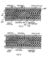
- the rigid section comprises a portion 41 having fibreglass epoxy layers 53, 42, 52 and 57 and copper layers 46 and 47.
- the flexible portion comprises polyimide layers 49, 43, and 48 and acrylic layers 51, 50, 45 and 44.
- Step A creates the smooth outer surface of the sandwich and Step B is the second processing step wherein the copper sheets are bonded to the smooth outer surfaces of the sandwich.
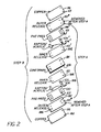
- the first layer is a bottom prepreg layer 100, on top of which are two smaller polyimide layers 104 of Kapton (Trade Mark), which overly cutouts 102 in the prepreg 100.
- Locating holes 101 are provided in each layer for precisely aligning the various layers.
- the locating holes 101 provided in the polyimide sheets 104, are positioned where they will not interfere with the printed circuit design.
- the surfaces of the polyimide layer 104 to be placed adjacent the prepreg 100 each have a layer of acrylic adhesive 106.
- a pair of conformal layers 108 which has the same approximate dimensions as the prepreg layer 100. Thus edge portions of the prepreg layer 100 and the conformal layer 108 abut each other without any intervening release layer.
- a second inner release layer 110', further polyimide layers 104' and a second prepreg layer 100' are provided on the outsides of the two prepreg layers 100,100'.
- additional release layers 110" On the outsides of the two prepreg layers 100,100' are provided additional release layers 110" which prevent adhesion of the prepreg layers 100,100' to the pressing plates.
- the polyimide layers 104,104' can be temporarily bonded to the release layer by localized application of heat and pressure around holes 105 to prevent lateral slippage of the polyimide with respect to the semi-rigid epoxy fibreglass layers 100,100' when assembling the sandwich for the first pressing operation.
- the first pressing operation partially cures the prepregs 100,100' and the conformals 108, and bonds all the curable layers together at their edges by pressing between a pair of steel sheets (not shown) to form a relatively rigid sandwich.
- the press is then opened, the outer release sheets 110" are removed and copper sheets 116,116' are positioned in the press by use of locating holes 117 and the pressing operation is continued at a higher temperature to bond the two copper layers firmly to the outer surfaces of the sandwich. Thereafter the two steel sheets are moved apart.
- the product can then be coated with a photo-resist and exposed to the necessary circuit diagram, the smooth copper surface lying in a single plane for accurate photo exposure. This exposure is preferably accomplished before disassembling the sandwich.
- the copper will have a smooth surface, since it was bonded in a ripple-free fashion, and can be held in a flat focal/plane.
- a sheet of fibreglass-epoxy prepreg 100 which is provided with an opening 102. Spanning the opening is a layer of polyimide 104 which overlaps the opening by approximately 1.27mm (0.050 inches).
- the outer surface of the polyimide is provided with a layer of acrylic adhesive 106.
- Behind the composite polyimide/fibreglass layer is a release layer 110 and then a conformal layer 108 which preferably is a flowable, curable fibreglass epoxy prepreg.
- the structure then follows the same order on the other side of the conformal 108.
- a pair of outer release layers 110" are provided.
- the purpose of the conformal is to fill in the space behind the polyimide film so as to compensate for the thinner polyimide sheet to force the upper surface of the polyimide sheet into conformance with a smooth surface of rigid plates 112.
- both the fibreglass prepreg and the conformal prepreg are partially cured so that they retain the shape obtained in the first pressing.
- the outer two release coats 110" are removed and replaced by two layers of copper 116 (see figure 4). Since the sandwich edges are sealed together, the various layer of the sandwich, comprising fibreglass-polyimide-conformal, remain as a relatively stiff unit. Pressing is then continued to bond the copper layers 116 to the outer surfaces of the sandwich.
- the two slightly smaller layers 110,11 0' of Teflon are provided, one on each side of the conformal, to prevent adhesion of the major portions of conformal to the outer layers of the sandwich so that the conformal can eventually be removed from the sandwich.
- adhesion between the rigid plates 112 and the fibreglass-polyimide acrylic system be prevented by use of release sheets 110" in the first pressing Step A.
- Fibreglass epoxy "No Flow" layers 100,100' are system "1080", in accordance with MIL-P13949, and are initially of the order of 0.076mm - 0.116mm (0.003 - 0.005 inches) thick.
- Polyimide layers 104,104' are preferably 0.025mm - 0.076mm (0.001 - 0.003 inch) thick DuPont Kapton.
- Acrylic adhesive 106 is on the order of 0.025mm - 0.076mm (0.001 - 0.003 inch) thick and is designated JW 712.
- Teflon release sheets 110,110' are preferably DuPont "superclean” grade TMR3, 0.025mm (0.001 inch) thick.
- Conformal prepreg 108 is preferably formed of two layers of fibreglass epoxy 1080 in accordance with the same specs as the fibreglass prepreg except that it is designated "High Flow” rather than "No Flow”. This permits the product of layer 108 to flow into the space adjacent the back of the polyimide sheet to permit creation of a smooth front surface.
- Copper sheets 116 are preferably IPC-CF-150 Type WRA. They are 0.107mm - 0.0174mm (0.0042 inch - .00075 inch, that is 3 ounce to 1/2 ounce), depending on the circuit requirements.
- the first pressing operation is conducted at 1.489 x 10 6 N.m- 2 (216 psi), and 127°C (250°F) for 30 minutes.
- the second pressing operation is carried out at the same pressure at 150°C - 182°C (300 - 360°F) for 60 minutes.
- the resulting sandwich, with the copper on the outside is removed from the press it is then treated in accordance with normal printed circuit technology. For example, it can be pumice cleaned.
- Photo-resist is then applied, the resist is exposed on both sides, the pattern is developed, the product is etched and optionally the copper is provided with a black oxide. Thereafter, the sealed "picture frame" edges are then cut and discarded to permit separation of the inner layers to remove the conformal layer and to provide a pair of rigid-flexible printed circuits.
Landscapes
- Engineering & Computer Science (AREA)
- Manufacturing & Machinery (AREA)
- Microelectronics & Electronic Packaging (AREA)
- Production Of Multi-Layered Print Wiring Board (AREA)
- Non-Metallic Protective Coatings For Printed Circuits (AREA)
- Structure Of Printed Boards (AREA)
- Polymers With Sulfur, Phosphorus Or Metals In The Main Chain (AREA)
Applications Claiming Priority (2)
| Application Number | Priority Date | Filing Date | Title |
|---|---|---|---|
| US565437 | 1990-08-09 | ||
| US07/565,437 US5095628A (en) | 1990-08-09 | 1990-08-09 | Process of forming a rigid-flex circuit |
Publications (3)
| Publication Number | Publication Date |
|---|---|
| EP0470740A2 true EP0470740A2 (fr) | 1992-02-12 |
| EP0470740A3 EP0470740A3 (fr) | 1992-12-30 |
| EP0470740B1 EP0470740B1 (fr) | 1995-01-11 |
Family
ID=24258595
Family Applications (1)
| Application Number | Title | Priority Date | Filing Date |
|---|---|---|---|
| EP91306862A Expired - Lifetime EP0470740B1 (fr) | 1990-08-09 | 1991-07-26 | Plaquette à circuit imprimé et méthode pour la formation de celle-ci |
Country Status (8)
| Country | Link |
|---|---|
| US (1) | US5095628A (fr) |
| EP (1) | EP0470740B1 (fr) |
| JP (1) | JP2832868B2 (fr) |
| AT (1) | ATE117160T1 (fr) |
| DE (1) | DE69106624T2 (fr) |
| DK (1) | DK0470740T3 (fr) |
| ES (1) | ES2066360T3 (fr) |
| GR (1) | GR3015668T3 (fr) |
Cited By (1)
| Publication number | Priority date | Publication date | Assignee | Title |
|---|---|---|---|---|
| WO1996018284A1 (fr) * | 1994-12-05 | 1996-06-13 | Teledyne Industries, Inc. | Fabrication de plaquettes de circuits imprimes rigides et souples combinees multicouches |
Families Citing this family (35)
| Publication number | Priority date | Publication date | Assignee | Title |
|---|---|---|---|---|
| US5147208A (en) * | 1991-06-28 | 1992-09-15 | Rogers Corporation | Flexible printed circuit with raised contacts |
| US5224023A (en) * | 1992-02-10 | 1993-06-29 | Smith Gary W | Foldable electronic assembly module |
| US5295838A (en) * | 1993-01-14 | 1994-03-22 | Hughes Aircraft Company | Raised feature/gold dot pressure interconnections of rigid-flex circuits and rigid circuit boards |
| US5428190A (en) * | 1993-07-02 | 1995-06-27 | Sheldahl, Inc. | Rigid-flex board with anisotropic interconnect and method of manufacture |
| US5376232A (en) * | 1993-08-23 | 1994-12-27 | Parlex Corporation | Method of manufacturing a printed circuit board |
| US5362534A (en) * | 1993-08-23 | 1994-11-08 | Parlex Corporation | Multiple layer printed circuit boards and method of manufacture |
| US5527998A (en) * | 1993-10-22 | 1996-06-18 | Sheldahl, Inc. | Flexible multilayer printed circuit boards and methods of manufacture |
| US5508558A (en) * | 1993-10-28 | 1996-04-16 | Digital Equipment Corporation | High density, high speed, semiconductor interconnect using-multilayer flexible substrate with unsupported central portion |
| US5877940A (en) * | 1993-12-02 | 1999-03-02 | Teledyne Industries Inc. | Fabrication multilayer combined rigid/flex printed circuit board |
| US6293008B1 (en) * | 1994-03-23 | 2001-09-25 | Dyconex Pantente Ag | Method for producing foil circuit boards |
| EP0675673A3 (fr) * | 1994-03-30 | 1997-03-05 | Nitto Denko Corp | Renforcement pour plaquette à circuit imprimé flexible et plaquette à circuit imprimé flexible renforcée. |
| US5499444A (en) * | 1994-08-02 | 1996-03-19 | Coesen, Inc. | Method of manufacturing a rigid flex printed circuit board |
| US5719749A (en) * | 1994-09-26 | 1998-02-17 | Sheldahl, Inc. | Printed circuit assembly with fine pitch flexible printed circuit overlay mounted to printed circuit board |
| US5629497A (en) * | 1994-10-04 | 1997-05-13 | Cmk Corporation | Printed wiring board and method of manufacturing in which a basefilm including conductive circuits is covered by a cured polyimide resin lay |
| JPH08107266A (ja) * | 1994-10-04 | 1996-04-23 | Cmk Corp | プリント配線板 |
| US5759047A (en) * | 1996-05-24 | 1998-06-02 | International Business Machines Corporation | Flexible circuitized interposer with apertured member and method for making same |
| US5784782A (en) * | 1996-09-06 | 1998-07-28 | International Business Machines Corporation | Method for fabricating printed circuit boards with cavities |
| US6099745A (en) * | 1998-06-05 | 2000-08-08 | Parlex Corporation | Rigid/flex printed circuit board and manufacturing method therefor |
| DE60143811D1 (de) * | 2000-10-16 | 2011-02-17 | Foster Miller Inc | Verfahren zur herstellung eines gewebeartikels mit elektronischer beschaltung und gewebeartikel |
| US6745463B1 (en) * | 2000-10-24 | 2004-06-08 | Unitech Printed Circuit Board Corp. | Manufacturing method of rigid flexible printed circuit board |
| DE10243637B4 (de) * | 2002-09-19 | 2007-04-26 | Ruwel Ag | Leiterplatte mit mindestens einem starren und mindestens einem flexiblen Bereich sowie Verfahren zur Herstellung von starr-flexiblen Leiterplatten |
| EP1659940B1 (fr) * | 2003-08-22 | 2014-07-23 | Foster-Miller, Inc. | Vetement de surveillance physiologique |
| US20070299325A1 (en) * | 2004-08-20 | 2007-12-27 | Brian Farrell | Physiological status monitoring system |
| KR101226541B1 (ko) * | 2004-08-31 | 2013-02-07 | 오베르메이어 헨리 케이 | 섬유 보강 복합물에 대한 고강력 결합 시스템 |
| KR100619347B1 (ko) * | 2004-10-28 | 2006-09-13 | 삼성전기주식회사 | 리지드-플렉서블 기판의 제조 방법 |
| US9211085B2 (en) | 2010-05-03 | 2015-12-15 | Foster-Miller, Inc. | Respiration sensing system |
| US9028404B2 (en) | 2010-07-28 | 2015-05-12 | Foster-Miller, Inc. | Physiological status monitoring system |
| US8585606B2 (en) | 2010-09-23 | 2013-11-19 | QinetiQ North America, Inc. | Physiological status monitoring system |
| US8683681B2 (en) * | 2010-12-07 | 2014-04-01 | Raytheon Company | Room temperature low contact pressure method |
| US10406791B2 (en) * | 2011-05-12 | 2019-09-10 | Elantas Pdg, Inc. | Composite insulating film |
| KR102042822B1 (ko) * | 2012-09-24 | 2019-11-08 | 한국전자통신연구원 | 전자회로 및 그 제조방법 |
| CN104582325B (zh) * | 2013-10-12 | 2018-03-27 | 鹏鼎控股(深圳)股份有限公司 | 刚挠结合板及其制作方法、电路板模组 |
| US10701799B2 (en) * | 2015-03-31 | 2020-06-30 | Hewlett-Packard Development Company, L.P. | Printed circuit board |
| US10595419B1 (en) | 2018-10-24 | 2020-03-17 | International Business Machines Corporation | 3-D flex circuit forming |
| CN113498249B (zh) * | 2020-04-07 | 2023-11-10 | 庆鼎精密电子(淮安)有限公司 | 软硬结合电路板及其制备方法 |
Family Cites Families (9)
| Publication number | Priority date | Publication date | Assignee | Title |
|---|---|---|---|---|
| US3393392A (en) * | 1966-04-27 | 1968-07-16 | Rca Corp | Printed circuit connector |
| US4001466A (en) * | 1973-11-27 | 1977-01-04 | Formica International Limited | Process for preparing printed circuits |
| US4037047A (en) * | 1974-12-31 | 1977-07-19 | Martin Marietta Corporation | Multilayer circuit board with integral flexible appendages |
| US4191800A (en) * | 1976-05-27 | 1980-03-04 | Bell Telephone Laboratories, Incorporated | Devices employing flexible substrates and method for making same |
| US4857400A (en) * | 1984-02-22 | 1989-08-15 | Gila River Products, Inc. | Stratiform press pads and methods for use thereof in laminating flexible printed circuits |
| DE3624719A1 (de) * | 1986-07-22 | 1988-01-28 | Schoeller & Co Elektronik | Vorlaminat fuer starr-flexible leiterplatten |
| US4800461A (en) * | 1987-11-02 | 1989-01-24 | Teledyne Industries, Inc. | Multilayer combined rigid and flex printed circuits |
| US4808461A (en) * | 1987-12-14 | 1989-02-28 | Foster-Miller, Inc. | Composite structure reinforcement |
| US4931134A (en) * | 1989-08-15 | 1990-06-05 | Parlex Corporation | Method of using laser routing to form a rigid/flex circuit board |
-
1990
- 1990-08-09 US US07/565,437 patent/US5095628A/en not_active Expired - Lifetime
-
1991
- 1991-04-12 JP JP3106570A patent/JP2832868B2/ja not_active Expired - Fee Related
- 1991-07-26 EP EP91306862A patent/EP0470740B1/fr not_active Expired - Lifetime
- 1991-07-26 ES ES91306862T patent/ES2066360T3/es not_active Expired - Lifetime
- 1991-07-26 DE DE69106624T patent/DE69106624T2/de not_active Expired - Lifetime
- 1991-07-26 AT AT91306862T patent/ATE117160T1/de not_active IP Right Cessation
- 1991-07-26 DK DK91306862.3T patent/DK0470740T3/da active
-
1995
- 1995-04-03 GR GR950400812T patent/GR3015668T3/el unknown
Cited By (1)
| Publication number | Priority date | Publication date | Assignee | Title |
|---|---|---|---|---|
| WO1996018284A1 (fr) * | 1994-12-05 | 1996-06-13 | Teledyne Industries, Inc. | Fabrication de plaquettes de circuits imprimes rigides et souples combinees multicouches |
Also Published As
| Publication number | Publication date |
|---|---|
| EP0470740B1 (fr) | 1995-01-11 |
| GR3015668T3 (en) | 1995-07-31 |
| ES2066360T3 (es) | 1995-03-01 |
| EP0470740A3 (fr) | 1992-12-30 |
| DK0470740T3 (da) | 1995-06-19 |
| JP2832868B2 (ja) | 1998-12-09 |
| DE69106624T2 (de) | 1995-08-10 |
| US5095628A (en) | 1992-03-17 |
| JPH06342980A (ja) | 1994-12-13 |
| DE69106624D1 (de) | 1995-02-23 |
| ATE117160T1 (de) | 1995-01-15 |
Similar Documents
| Publication | Publication Date | Title |
|---|---|---|
| EP0470740B1 (fr) | Plaquette à circuit imprimé et méthode pour la formation de celle-ci | |
| US5175047A (en) | Rigid-flex printed circuit | |
| US5633480A (en) | Printed wiring board having a cover lay laminated on a polyimide resin base film containing conductive circuits | |
| WO1993011652A1 (fr) | Combinaison de circuits imprimes et procede relatif a celle-ci | |
| JPH08139455A (ja) | リジットフレキシブルプリント配線板 | |
| JPH06204663A (ja) | プリント配線板の製造方法 | |
| JPH098457A (ja) | フレックスリジッド配線板の製造方法 | |
| JP2004153000A (ja) | プリント基板の製造方法およびそれにより製造されるプリント基板 | |
| JP2006216593A (ja) | リジッドフレックス多層配線板の製造方法 | |
| JP2609298B2 (ja) | 多層積層板の製造方法 | |
| JPH08107273A (ja) | プリント配線板の製造方法 | |
| JP3962119B2 (ja) | 多層プリント配線板製造用シート | |
| JPH07105599B2 (ja) | フレキシブルリジッドプリント板の製造方法 | |
| JPH06152136A (ja) | プリント配線板の製造方法 | |
| JP2864276B2 (ja) | プリント配線基板の製造方法 | |
| JP2583964B2 (ja) | 補強板付フレキシブルプリント配線板およびその製造法 | |
| JP3934826B2 (ja) | 多層配線板の製造方法 | |
| JPH06268354A (ja) | フレキシブル回路基板の製造方法 | |
| JPH0728127B2 (ja) | 多層回路積層板の製造方法 | |
| JP2000307247A (ja) | リジッドフレキシブル多層プリント配線板の製造法 | |
| JPH07135393A (ja) | リジッドフレキシブル多層プリント板 | |
| JPH05243708A (ja) | 補強板付きフレキシブルプリント配線板の製造方法 | |
| JP2568002B2 (ja) | フレキシブルプリント回路基板及びその製造方法 | |
| JPH0349290A (ja) | フレキシブルプリント配線板及びその製造方法 | |
| JPH08335758A (ja) | プリント配線板およびその製造方法 |
Legal Events
| Date | Code | Title | Description |
|---|---|---|---|
| PUAI | Public reference made under article 153(3) epc to a published international application that has entered the european phase |
Free format text: ORIGINAL CODE: 0009012 |
|
| AK | Designated contracting states |
Kind code of ref document: A2 Designated state(s): AT BE CH DE DK ES FR GB GR IT LI LU NL SE |
|
| PUAL | Search report despatched |
Free format text: ORIGINAL CODE: 0009013 |
|
| AK | Designated contracting states |
Kind code of ref document: A3 Designated state(s): AT BE CH DE DK ES FR GB GR IT LI LU NL SE |
|
| 17P | Request for examination filed |
Effective date: 19930625 |
|
| 17Q | First examination report despatched |
Effective date: 19940126 |
|
| GRAA | (expected) grant |
Free format text: ORIGINAL CODE: 0009210 |
|
| AK | Designated contracting states |
Kind code of ref document: B1 Designated state(s): AT BE CH DE DK ES FR GB GR IT LI LU NL SE |
|
| ITF | It: translation for a ep patent filed | ||
| REF | Corresponds to: |
Ref document number: 117160 Country of ref document: AT Date of ref document: 19950115 Kind code of ref document: T |
|
| REF | Corresponds to: |
Ref document number: 69106624 Country of ref document: DE Date of ref document: 19950223 |
|
| REG | Reference to a national code |
Ref country code: ES Ref legal event code: FG2A Ref document number: 2066360 Country of ref document: ES Kind code of ref document: T3 |
|
| ET | Fr: translation filed | ||
| REG | Reference to a national code |
Ref country code: DK Ref legal event code: T3 |
|
| REG | Reference to a national code |
Ref country code: GR Ref legal event code: FG4A Free format text: 3015668 |
|
| PGFP | Annual fee paid to national office [announced via postgrant information from national office to epo] |
Ref country code: LU Payment date: 19950801 Year of fee payment: 5 |
|
| PLBE | No opposition filed within time limit |
Free format text: ORIGINAL CODE: 0009261 |
|
| STAA | Information on the status of an ep patent application or granted ep patent |
Free format text: STATUS: NO OPPOSITION FILED WITHIN TIME LIMIT |
|
| 26N | No opposition filed | ||
| PG25 | Lapsed in a contracting state [announced via postgrant information from national office to epo] |
Ref country code: LU Free format text: LAPSE BECAUSE OF NON-PAYMENT OF DUE FEES Effective date: 19960726 |
|
| PGFP | Annual fee paid to national office [announced via postgrant information from national office to epo] |
Ref country code: ES Payment date: 20000808 Year of fee payment: 10 |
|
| PGFP | Annual fee paid to national office [announced via postgrant information from national office to epo] |
Ref country code: DK Payment date: 20010704 Year of fee payment: 11 |
|
| PG25 | Lapsed in a contracting state [announced via postgrant information from national office to epo] |
Ref country code: ES Free format text: LAPSE BECAUSE OF NON-PAYMENT OF DUE FEES Effective date: 20010727 |
|
| PGFP | Annual fee paid to national office [announced via postgrant information from national office to epo] |
Ref country code: GR Payment date: 20010731 Year of fee payment: 11 |
|
| REG | Reference to a national code |
Ref country code: GB Ref legal event code: IF02 |
|
| PG25 | Lapsed in a contracting state [announced via postgrant information from national office to epo] |
Ref country code: DK Free format text: LAPSE BECAUSE OF NON-PAYMENT OF DUE FEES Effective date: 20020731 |
|
| PG25 | Lapsed in a contracting state [announced via postgrant information from national office to epo] |
Ref country code: GR Free format text: LAPSE BECAUSE OF NON-PAYMENT OF DUE FEES Effective date: 20030206 |
|
| REG | Reference to a national code |
Ref country code: DK Ref legal event code: EBP |
|
| REG | Reference to a national code |
Ref country code: ES Ref legal event code: FD2A Effective date: 20020810 |
|
| REG | Reference to a national code |
Ref country code: FR Ref legal event code: TP |
|
| REG | Reference to a national code |
Ref country code: GB Ref legal event code: 732E |
|
| REG | Reference to a national code |
Ref country code: CH Ref legal event code: PUE Owner name: TELEDYNE TECHNOLOGIES INCORPORATED Free format text: TELEDYNE INDUSTRIES, INC.#1901 AVENUE OF THE STARS#LOS ANGELES/CA (US) -TRANSFER TO- TELEDYNE TECHNOLOGIES INCORPORATED#12333 WEST OLYMPIC BOULEVARD#LOS ANGELES, CA 90064 (US) |
|
| BECA | Be: change of holder's address |
Owner name: *TELEDYNE TECHNOLOGIES INC.12333 WEST OLYMPIC BOUL Effective date: 20050217 |
|
| NLS | Nl: assignments of ep-patents |
Owner name: TELEDYNE TECHNOLOGIES INCORPORATED, A DELAWARE COR |
|
| BECA | Be: change of holder's address |
Owner name: *TELEDYNE TECHNOLOGIES INC.12333 WEST OLYMPIC BOUL Effective date: 20050217 |
|
| PGFP | Annual fee paid to national office [announced via postgrant information from national office to epo] |
Ref country code: NL Payment date: 20100724 Year of fee payment: 20 Ref country code: CH Payment date: 20100726 Year of fee payment: 20 |
|
| PGFP | Annual fee paid to national office [announced via postgrant information from national office to epo] |
Ref country code: FR Payment date: 20100805 Year of fee payment: 20 Ref country code: DE Payment date: 20100728 Year of fee payment: 20 Ref country code: IT Payment date: 20100728 Year of fee payment: 20 Ref country code: SE Payment date: 20100728 Year of fee payment: 20 Ref country code: AT Payment date: 20100702 Year of fee payment: 20 |
|
| PGFP | Annual fee paid to national office [announced via postgrant information from national office to epo] |
Ref country code: GB Payment date: 20100726 Year of fee payment: 20 |
|
| PGFP | Annual fee paid to national office [announced via postgrant information from national office to epo] |
Ref country code: BE Payment date: 20100728 Year of fee payment: 20 |
|
| REG | Reference to a national code |
Ref country code: CH Ref legal event code: PFA Owner name: TELEDYNE TECHNOLOGIES INCORPORATED Free format text: TELEDYNE TECHNOLOGIES INCORPORATED#12333 WEST OLYMPIC BOULEVARD#LOS ANGELES, CA 90064 (US) -TRANSFER TO- TELEDYNE TECHNOLOGIES INCORPORATED#12333 WEST OLYMPIC BOULEVARD#LOS ANGELES, CA 90064 (US) |
|
| REG | Reference to a national code |
Ref country code: DE Ref legal event code: R071 Ref document number: 69106624 Country of ref document: DE |
|
| REG | Reference to a national code |
Ref country code: DE Ref legal event code: R071 Ref document number: 69106624 Country of ref document: DE |
|
| BE20 | Be: patent expired |
Owner name: *TELEDYNE TECHNOLOGIES INC. Effective date: 20110726 |
|
| REG | Reference to a national code |
Ref country code: NL Ref legal event code: V4 Effective date: 20110726 |
|
| REG | Reference to a national code |
Ref country code: CH Ref legal event code: PL |
|
| REG | Reference to a national code |
Ref country code: GB Ref legal event code: PE20 Expiry date: 20110725 |
|
| REG | Reference to a national code |
Ref country code: SE Ref legal event code: EUG |
|
| PG25 | Lapsed in a contracting state [announced via postgrant information from national office to epo] |
Ref country code: GB Free format text: LAPSE BECAUSE OF EXPIRATION OF PROTECTION Effective date: 20110725 |
|
| PG25 | Lapsed in a contracting state [announced via postgrant information from national office to epo] |
Ref country code: NL Free format text: LAPSE BECAUSE OF EXPIRATION OF PROTECTION Effective date: 20110726 |
|
| PG25 | Lapsed in a contracting state [announced via postgrant information from national office to epo] |
Ref country code: DE Free format text: LAPSE BECAUSE OF EXPIRATION OF PROTECTION Effective date: 20110727 |