EP0470827A2 - Circuit de sélection de signal de synchronisation - Google Patents
Circuit de sélection de signal de synchronisation Download PDFInfo
- Publication number
- EP0470827A2 EP0470827A2 EP91307254A EP91307254A EP0470827A2 EP 0470827 A2 EP0470827 A2 EP 0470827A2 EP 91307254 A EP91307254 A EP 91307254A EP 91307254 A EP91307254 A EP 91307254A EP 0470827 A2 EP0470827 A2 EP 0470827A2
- Authority
- EP
- European Patent Office
- Prior art keywords
- signal
- pulse
- synchronizing signal
- sync signal
- composite
- Prior art date
- Legal status (The legal status is an assumption and is not a legal conclusion. Google has not performed a legal analysis and makes no representation as to the accuracy of the status listed.)
- Granted
Links
Images




Classifications
-
- H—ELECTRICITY
- H04—ELECTRIC COMMUNICATION TECHNIQUE
- H04N—PICTORIAL COMMUNICATION, e.g. TELEVISION
- H04N5/00—Details of television systems
- H04N5/04—Synchronising
- H04N5/08—Separation of synchronising signals from picture signals
- H04N5/10—Separation of line synchronising signal from frame synchronising signal or vice versa
Definitions
- the present invention relates to a synchronizing signal selection circuit, and more particularly to a synchronizing signal selection circuit for extracting the timing of a horizontal synchronizing signal from a composite synchronizing signal.
- synchronizing signal is abbreviated as "sync signal”.
- a composite sync signal in which a vertical sync signal and horizontal sync signal are combined is supplied as a sync signal to a television apparatus.
- this composite sync signal is obtained by separating it from a composite video signal carried on a transmitted broadcast wave.
- a clock signal for sampling image signals in the LCD apparatus is generated. Since this clock signal must be precisely synchronous with the horizontal sync signal when display is performed based on the image information in the above-mentioned television system, the clock signal is generated using a PLL (Phase-Locked Loop) circuit 100 as shown in Figure 8.
- the PLL circuit 100 has a loop which comprises a voltage-controlled oscillator (VCO) 101, a frequency divider 102, a phase comparator 103 and a low-pass filter (LPF) 104. It is desirable to supply the horizontal sync signal as the sync signal Sync which is the input signal of the PLL circuit 100. In the prior art, however, the composite sync signal is supplied as it is.
- Figures 9A to 9C show composite sync signals used in the NTSC system.
- Figure 9A shows a composite sync signal in a transition period from an even field to an odd field.
- Figure 9B shows a portion of a composite sync signal in one field.
- Figure 9C a composite sync signal in a transition period from an odd field to an even field is shown.
- a vertical sync signal and an equalizing pulse 22 exist in the composite sync signal in the transition period from one field to the next field.
- the equalizing pulse 22 is inserted to equalize the waveforms of the composite sync signal in the portion of the vertical sync signal and in the peripheral portion thereof, during the transition period from the even field to the odd field and during the transition period from the odd field to the even field.
- the width of the horizontal sync signal 21 and that of the equalizing pulse 22 are half as compared with that of the normal horizontal sync signal 21.
- an AGC Auto Gain Control
- the AGC signal cannot be completely removed by a low-pass filter in the extraction of the composite sync signal from the composite video signal, and therefore, a pulse (which may be a spurious sync signal such as that shown in Figure 10) is mixed in immediately after the vertical sync signal in the extracted composite sync signal.
- this horizontal sync signal separation circuit has a slight imperfection in which the image quality quickly deteriorates as a result of discontinuous degradation of the quality of the separated horizontal sync signal.
- the synchronizing signal selection circuit of this invention which overcomes the above-discussed and numerous other disadvantages and deficiencies of the prior art, comprises: control signal generation means for, in response to the input of a vertical synchronizing signal extracted from a composite synchronizing signal, generating a control signal which is in a predetermined state during a certain period, said period beginning when a first predetermined time period has elapsed after said input of said vertical synchronizing signal and terminating when a second predetermined time period has elapsed after said input of said vertical synchronizing signal; and selection means for receiving said composite synchronizing signal, a horizontal synchronizing signal separated from said composite synchronizing signal, and said control signal, and for outputting said composite synchronizing signal when said control signal is in said predetermined state, and outputting said separated horizontal synchronizing signal when said control signal is in a state other than said predetermined state.
- said first predetermined time period is shorter than said second predetermined time period.
- said control signal generation means comprises: counting means for receiving a periodic pulse string, and for counting the number of pulses contained in said periodic pulse string; and decoding means coupled to the output of said counting means, for, when the output of said counting means becomes a first predetermined value, setting said control signal to said predetermined state, said first predetermined value corresponding to said first predetermined time period, and for, when the output of said counting means becomes a second predetermined value, setting said control signal to a state other than said predetermined state, said second predetermined value corresponding to said second predetermined time period.
- said counting means is reset by the rising edge of said vertical synchronizing signal.
- said control signal generation means comprises: first pulse signal generation means for, in response to the input of said vertical synchronizing signal, generating a first pulse signal, said first pulse signal ending when said first predetermined time period has elapsed after said input of the vertical synchronizing signal; second pulse signal generation means for, in response to said input of said vertical synchronizing signal, generating a second pulse signal, said second pulse signal ending when said second predetermined time period has elapsed after said input of said vertical synchronizing signal; and means for generating said control signal, based on said first and second pulse signals.
- said control signal generation means may comprise: first pulse signal generation means for, in response to said input of said vertical synchronizing signal, generating a first pulse signal, said first pulse signal ending when said first predetermined time period has elapsed after said input of said vertical synchronizing signal; second pulse signal generation means for, in response to the end of said first pulse signal, generating a second signal pulse signal, said second pulse signal ending when said second predetermined time period has elapsed after said end of said first pulse signal; and means for generating said control signal, based on said first and second pulse signals.
- Figure 1 is a block diagram showing a sync signal selection circuit in a first embodiment of the invention.
- Figure 2 is a timing chart illustrating the operation of the first embodiment.
- Figure 3 is a block diagram showing an example of a horizontal sync signal separation circuit used in conjunction with the sync signal selection circuit of the invention.
- Figure 4 is a timing chart illustrating the operation of the horizontal sync signal separation circuit of Figure 3 in a case that a pulse caused by noise is mixed into a composite sync signal.
- Figure 5 is a circuit diagram illustrating a second embodiment of the invention.
- Figure 6 is a circuit diagram illustrating a third embodiment of the invention.
- Figure 7 shows an example of a horizontal sync signal obtained from a composite sync signal by the sync signal selection circuit of the invention and the horizontal sync signal separation circuit shown in Figure 3.
- Figure 8 is a block diagram showing a PLL circuit used for generating a sampling clock in a prior art LCD apparatus.
- Figures 9A to 9C show composite sync signals used in the NTSC system.
- Figure 10 shows a composite sync signal obtained from a video tape which was subjected to a duplication prevention process.
- Figure 11 is a block diagram showing a fourth embodiment of the invention.
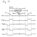
- Figure 12 is a timing chart illustrating the operation of the fourth embodiment.
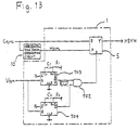
- Figure 13 is a block diagram showing an example of the variation of the fourth embodiment.
- Figure 14 is a block diagram showing a fifth embodiment of the invention.
- Figure 15 is a timing chart illustrating the operation of the fifth embodiment.
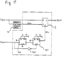
- Figures 16 and 17 are block diagrams showing examples of variations of the fifth embodiment.
- FIG. 1 is a block diagram of a first embodiment of the invention.
- a sync signal selection circuit 1 in Figure 1 comprises a counter 2, a decoder 3, an RS flip-flop 4 and a selector 5.
- the counter 2, the decoder 3 and the RS flip-flop 4 function together as a signal generation circuit for generating a selection signal SEL.
- a vertical sync signal V syn separated from a composite sync signal C sync is input to the clear terminal CL of the counter 2.
- the counter 2 is cleared by the rising edge of the vertical sync signal V syn .
- a circuit for separating the vertical sync signal V syn from the composite sync signal C sync is known from the Television Institute's publication, "Television" (Corona Publishing Co., Ltd, Japan.).
- a signal HSYO which is a periodic pulse string is input to the clock terminal CK of the counter 2.
- the counter 2 starts to count the pulses in the signal HSYO, immediately after being cleared, and the count result is supplied to the decoder 3.
- the decoder 3 outputs a set signal T S when the count result indicates a first predetermined value after a first predetermined time period has elapsed from when the counter 2 was cleared.
- the decoder 3 also outputs a reset signal T R when the count result indicates a second predetermined value after a second predetermined time period has elapsed from when the counter 2 was cleared.
- the set signal T S and the reset signal T R are supplied to the set terminal S and the reset terminal R, respectively, of the RS flip-flop 4. Therefore, a selection signal SEL output from the RS flip-flop 4 is set by the set signal T S to be HIGH, and is reset by the reset signal T R to be LOW.
- the composite sync signal C sync and a horizontal sync signal H syn obtained from the composite sync signal C sync by a horizontal sync signal separation circuit 10 are input to a terminal B and a terminal A, respectively, of the selector 5.
- the selection signal SEL is input to a terminal S of the selector 5.
- the selector 5 selectively outputs as a horizontal sync signal HSYN the composite sync signal C sync when the selection signal SEL is HIGH, and selectively outputs the separated horizontal sync signal H syn when the selection signal SEL is LOW.
- the signal HSYN output from the selector 5 becomes the horizontal sync signal that is finally used.
- the period from one vertical sync signal 25 to the next vertical sync signal 25 is the scanning period for one field, but the display period during which display is actually performed is a part of the scanning period as shown in Figure 2.
- the display period begins after a period of time T B has elapsed from the rising edge of the vertical sync signal 25, and it is completed after a period of time T E has elapsed.
- the first predetermined time period is set slightly shorter than the period of time T B
- the second predetermined time period is set slightly longer than the period of time T E . Therefore, the decoder 3 outputs the set signal T S immediately before the start of the display period and outputs the reset signal T R immediately after the completion of the display period.
- the selection signal SEL becomes HIGH during the display period, and becomes LOW during all other periods, i.e., during the vertical retrace line vertical. Therefore, the composite sync signal C sync is output from the selector 5 as the horizontal sync signal HSYN during the display period, and the separated horizontal sync signal H syn is output from the selector 5 as the horizontal sync signal HSYN during the vertical retrace line interval.
- the composite sync signal C sync is input to a rising edge detection circuit 11.
- the rising edge detection circuit 11 detects the rise of the composite sync signal C sync , it supplies a pulse signal HED to one input terminal of an AND gate 12.
- a counter 13 counts the number of pulses in the clock signal CLK.
- the output of the counter 13 is supplied to a decoder 14.
- the decoder 14 decodes the output of the counter 13 to output three timing signals t1, t2 and t3.
- the timing signals t1 and t2 are input to the set terminal S and the reset terminal R of an RS flip-flop 15, respectively.
- An output signal TPF of the RS flip-flop 15 is supplied to the other input terminal of the AND gate 12, and the pulse signal HED passes through the AND gate 12 while the signal TPF is HIGH. That is, the signal TPF is a control signal for the AND gate 12, and this control signal TPF is generated by the decoder 14 and the RS flip-flop 15 based on the output of the counter 13.
- the output of the AND gate 12 i.e., the signal HED that passes through the AND gate 12
- the timing signal t3 is supplied to the reset terminal R of an RS flip-flop 16.
- the output of the AND gate 12 is supplied to the set terminal S of the RS flip-flop 16.
- the composite sync signal C sync and a signal IH syn output from the RS flip-flop 16 are input to the two input terminals of an AND gate 17, respectively.
- the separated horizontal sync signal H syn is output from the AND gate 17.
- the rise of the pulse in the separated horizontal sync signal H syn essentially corresponds with the passage of the pulse signal HED through the AND gate 12 by the action of the RS flip-flop 16 and the AND gate 17.
- FIG 4 shows the composite sync signal C sync containing noise, and the control signal TPF, the signal IH syn and the separated horizontal sync signal H syn which are generated in the horizontal sync signal separation circuit 10 ( Figure 3) when the composite sync signal C sync containing noise is input.
- the composite sync signal C sync also contains pulses 41, 42, 43 and 44 caused by noise, in addition to the horizontal sync signal 21. Of these pulses, the pulses 41 and 42 do not affect the separated horizontal sync signal H syn , because they are removed by the control signal TPF.
- the pulses 43 and 44 are generated during the period when the control signal TPF is HIGH, they do affect the separated horizontal sync signal H syn .
- the pulse 43 causes the separated horizontal sync signal H syn to lose much of the waveform of the original horizontal sync signal 21 in the composite sync signal C sync .
- the original horizontal sync signal 21 may become completely nonexistent in the separated horizontal sync signal H syn due to pulse caused by noise.
- the PLL circuit to which the separated horizontal sync signal H syn is input is greatly affected, resulting in large shifts in the phase of the clock signal output from the PLL circuit.
- the separated horizontal sync signal obtained by the horizontal sync signal separation circuit 10 i.e., the horizontal sync signal H syn obtained by removing the vertical sync signal and equalizing pulse contained in the composite sync signal
- the horizontal sync signal HSYN only during the vertical retrace line interval during which the waveform of the composite sync signal C sync differs greatly from that of the horizontal sync signal 21.
- the composite sync signal C sync is output as the horizontal sync signal HSYN. Therefore, the quality of the horizontal sync signal HSYN does not fall below that of the original composite sync signal C sync , and resistance to noise in cases of high noise levels is improved.
- Figure 5 shows a second embodiment of the invention.
- the vertical sync signal V syn is input to the clear terminal CL of the counter 2 via a rising edge detection circuit 6.
- the rising edge detection circuit 6 comprises a resistor 651, a capacitor 652, a buffer 653, an inverter 654 and an AND gate 655.
- the counter 2 is a binary counter.
- the second, fifth and ninth outputs Q2, Q5 and Q9 of the counter 2 are supplied to the decoder 3.
- the output of a frequency divider 102 of a PLL circuit 100 similar to that in Figure 8 is used as the signal HSYO input to the clock terminal CK of the counter 2.
- the horizontal sync signal HSYN from the selector 5 is input to a phase comparator 103 of the PLL circuit 100. Since the separated horizontal sync signal H syn may contain pulses caused by noise as described above, it is not preferable to use the separated horizontal sync signal H syn as the signal HSYO.
- the decoder 3 comprises a NAND gate 351 which outputs the set signal T S , and an inverter 352 which outputs the reset signal T R .
- the outputs Q2 and Q5 of the counter 2 are input to the NAND gate 351. Therefore, the set signal T S is output when the value of the output of the counter 2 becomes 18 (decimal).
- the selection signal SEL becomes HIGH in response to the set signal T S .
- the output Q9 of the counter 2 is supplied to the inverter 352. Therefore, the reset signal T R is output when the value of the output of the counter 2 becomes 256 (decimal).
- the selection signal SEL becomes LOW in response to the reset signal T R .
- Figure 6 shows a third embodiment of the invention.
- components similar to those of the sync signal selection circuit 1 in Figure 1 are designated by the same reference numerals as those in Figure 1.
- a rising edge detection circuit 66 comprising a D-type flip-flop 661, an AND gate 662 and an inverter 663 is used in place of the rising edge detection circuit 6 in Figure 5.
- the signal HSYO obtained by the PLL circuit 100 in the same way as in Figure 5 is supplied to the clock terminal CK of the D-type flip-flop 661 via the inverter 663.
- a decoder 36 comprising a NAND gate 361 and a NOR gate 362 is used in place of the decoder 3 in Figure 5.
- the NAND gate 361 functions in the same manner as the NAND gate 351 in Figure 5.
- the output Q9 of the counter 2 and the output of the rising edge detection circuit 66 are input to the NOR gate 362 for outputting the reset signal T R .
- the reset signal T R is output and that the selection signal SEL is returned to LOW, even if the next rising edge of the vertical sync signal V syn is detected before the value of the output of the counter 2 reaches 256.
- the next rising edge of the vertical sync signal V syn may be detected before the value of the output of the counter 2 reaches 256.
- This embodiment normally functions even in such a case.
- Figure 7 shows the composite sync signal C sync into which a spurious sync signal similar to that in Figure 10 is mixed, and the horizontal sync signal HSYN obtained from the composite sync signal C sync by the combination of the horizontal sync signal separation circuit shown in Figure 3 and the sync signal selection circuit shown in Figure 5.
- the separated horizontal sync signal H syn output from the horizontal sync signal separation circuit is output as the horizontal sync signal HSYN during the vertical retrace line vertical.
- the composite sync signal C sync is output as it is as the horizontal sync signal HSYN.
- the vertical sync signal and equalizing pulse exist in the composite sync signal and a spurious sync signal is mixed with the composite sync signal only during the vertical retrace line vertical. Therefore, the use of the composite sync signal C sync as it is during the display period according to the invention conforms with the nature of the composite sync signal.
- FIG 11 shows a fourth embodiment of the invention.
- the sync signal selection circuit 1 of this embodiment comprises a first pulse generation circuit PG1 and a second pulse generation circuit PG2.
- the pulse generation circuits PG1 and PG2 generate pulses from the outputs Q in synchronous with the potential rise at their inputs B.
- the vertical sync signal V syn separated from the composite sync signal C sync is input to the inputs B of the pulse generation circuits PG1 and PG2.
- the output Pulse1 of the first pulse generation circuit PG1 is coupled to one input terminal of an AND gate 702 via an inverter 701.
- the output Pulse2 of the second pulse generation circuit PG2 is directly connected to the other input terminal of the AND gate 702.
- the output of the AND gate 702 is input to the terminal S of the selector 5 as the selection signal SEL.
- the period from one vertical sync signal 25 to the next vertical sync signal 25 is the scanning period for one field, but the display period during which display is actually performed is a part of the scanning period as shown in Figure 12.
- the display period starts after the period of time T B has elapsed from the rising edge of the vertical sync signal 25, and ends after the period time T E has elapsed.
- the pulse Pulse1 is generated by the first pulse generation circuit PG1 so that its pulse width is approximately equal to the period time T B .
- the pulse Pulse2 is generated by the second pulse generation circuit PG2 so that its pulse width is approximately equal to the period of time T E .
- the selection signal SEL output from the AND gate 702 is HIGH only during the display period in the scanning period of one field. For this reason, the composite sync signal C sync is selected and output as the output of the selector 5 during the display period, and the horizontal sync signal H syn separated by the horizontal sync signal separation circuit 10 is selected and output during the period other than the display period.
- Figure 13 shows the circuit diagram of a configuration in which the first pulse generation circuit PG1 and the second pulse generation circuit PG2 in the embodiment of Figure 11 are realized by two monostable multivibrators 703 and 704.
- the inverter 701 in Figure 11 is not used, and the pulse Pulse1 ⁇ is obtained directly from the output of the inverted logic output Q ⁇ of the monostable multivibrator 703.
- the width of each of the pulses is determined by appropriately setting the time constants determined by capacitors C1 and C2 and resistors R1 and R2. Generally, error is large in the control of the pulse widths determined by the time constant of C and R. Since it is not necessary to strictly control the widths of the pulses Pulse1 and Pulse2 as described below, there is no problem in practical application even if the pulse widths are predetermined by the time constant of C and R.
- Figure 14 shows a fifth embodiment of the invention.
- the output of the first pulse generation circuit PG1 is input to the second pulse generation circuit PG2 via an inverter 705, and the output of the second pulse generation circuit PG2 is input to the terminal S of the selector 5.
- T B is the time period from the rise of the vertical sync signal V syn to the beginning of the display period
- T DIS is the display period.
- the first pulse generation circuit PG1 generates the pulse Pulse1 of width T B from the rise of the vertical sync signal V syn
- the second pulse generation circuit PG2 generates the pulse Pulse2 of width T DIS from the rising edge of the inverted signal Pulse1 ⁇ of the pulse Pulse1 (i.e., the falling edge of the pulse Pulse1).
- This Pulse2 is supplied as it is as the selection signal SEL to the terminal S of the selector 5. Therefore, the composite signal C sync is selected and output as the output of the selector 5 during the display period, and the horizontal sync signal H syn separated by the horizontal sync signal separation circuit 10 is selected and output during the period other than the display period.
- the HIGH-level period of the selection signal SEL shown in Figures 12 and 15 coincides with the display period. That is, it is desirable that the rising and falling positions of the selection signal SEL agree with the start position and the end position of the display period, respectively.
- the HIGH-level period of the selection signal SEL occupies the major portion of the display period. Therefore, it is no necessary to strictly control the widths of the pulses Pulse1 and Pulse2.
- Figure 16 shows the circuit diagram of a configuration in which the first and second pulse generation circuits PG1 and PG2 in the embodiment of Figure 14 are realized by monostable multivibrators 706 and 707.
- the inverter 705 in Figure 14 is not used, and the pulse Pulse1 ⁇ is obtained directly from the output of the inverted logic output Q ⁇ of the monostable multivribrator 706.
- FIG 17 shows a variation of the example in Figure 16.
- the vertical sync signal V syn is input to the CLR input of the monostable multivribrator 707 via an inverter 708. Even if the next rise of the vertical sync signal V syn occurs while the output of the monostable multivribrator 707 (i.e., the selection signal SEL) is HIGH, the multivribrator 707 is reset at this time. Therefore, the horizontal sync signal H syn is output from the selector 5 as the horizontal sync signal HSYN from that time until the next rise of the selection signal SEL.
- the vertical sync signal contained in the composite sync signal C sync , or the spurious sync signal shown in Figure 10 can be prevented from being output as the horizontal sync signal HSYN. This may occur when a signal different from a regular NTSC signal is input as the composite video signal as in special effect playback (high speed search, pause, etc.) of video tapes, but this embodiment functions normally even under these conditions.
- a sync signal selection circuit is provided that is capable of obtaining a good horizontal sync signal from the composite sync signal, even in cases in which pulses and other signals caused by noise are mixed in the composite sync signal, by selectively using the composite sync signal and the horizontal sync signal separated from the composite sync signal.
- the sync signal selection circuit of the invention the high resistance to noise can be achieved in a display apparatus such as an LCD apparatus in which it is necessary to obtain a sampling clock signal from the composite sync signal.
- the invention can not only solve problems in video playback, but it also can contribute greatly to improved overall performance and display quality in an LCD apparatus.
Landscapes
- Engineering & Computer Science (AREA)
- Multimedia (AREA)
- Signal Processing (AREA)
- Synchronizing For Television (AREA)
Applications Claiming Priority (4)
| Application Number | Priority Date | Filing Date | Title |
|---|---|---|---|
| JP21060890 | 1990-08-08 | ||
| JP210608/90 | 1990-08-08 | ||
| JP261482/90 | 1990-09-28 | ||
| JP2261482A JP2685643B2 (ja) | 1990-08-08 | 1990-09-28 | 同期信号選択回路 |
Publications (3)
| Publication Number | Publication Date |
|---|---|
| EP0470827A2 true EP0470827A2 (fr) | 1992-02-12 |
| EP0470827A3 EP0470827A3 (en) | 1992-07-01 |
| EP0470827B1 EP0470827B1 (fr) | 1995-07-12 |
Family
ID=26518154
Family Applications (1)
| Application Number | Title | Priority Date | Filing Date |
|---|---|---|---|
| EP91307254A Expired - Lifetime EP0470827B1 (fr) | 1990-08-08 | 1991-08-07 | Circuit de sélection de signal de synchronisation |
Country Status (3)
| Country | Link |
|---|---|
| US (1) | US5245431A (fr) |
| EP (1) | EP0470827B1 (fr) |
| DE (1) | DE69111152T2 (fr) |
Families Citing this family (12)
| Publication number | Priority date | Publication date | Assignee | Title |
|---|---|---|---|---|
| JP2919278B2 (ja) * | 1994-09-14 | 1999-07-12 | 日本電気株式会社 | マルチシンク対応液晶ディスプレイ装置の表示制御装置及び表示制御方法 |
| US5610667A (en) * | 1995-08-24 | 1997-03-11 | Micron Display Technology, Inc. | Apparatus and method for maintaining synchronism between a picture signal and a matrix scanned array |
| US5635988A (en) * | 1995-08-24 | 1997-06-03 | Micron Display Technology, Inc. | Apparatus and method for maintaining synchronism between a picture signal and a matrix scanned array |
| KR0170730B1 (ko) * | 1996-01-12 | 1999-03-20 | 김광호 | 필드 동기신호 검출회로 및 그 방법 |
| EP0809409B1 (fr) * | 1996-05-24 | 2001-08-29 | Matsushita Electric Industrial Co., Ltd. | Procédé et circuit pour déterminer une valeur du bruit représentative du bruit dans un signal |
| US5854615A (en) * | 1996-10-03 | 1998-12-29 | Micron Display Technology, Inc. | Matrix addressable display with delay locked loop controller |
| JPH11355603A (ja) * | 1998-06-09 | 1999-12-24 | Fuji Film Microdevices Co Ltd | 水平同期検出回路 |
| DE19908071C2 (de) * | 1999-02-12 | 2001-08-02 | Lear Automotive Electronics Gm | Verfahren zur Stabilisierung der Horizontal- und Vertikalsynchronimpulse eines empfangenen Fernsehsignals und Schaltung zur Durchführung des Verfahrens |
| US6298100B1 (en) * | 1999-10-26 | 2001-10-02 | Thomson Licensing S.A. | Phase error estimation method for a demodulator in an HDTV receiver |
| US7282532B2 (en) * | 2003-06-06 | 2007-10-16 | M Management-Tex, Ltd. | Flexible bakeware |
| JP4149430B2 (ja) * | 2003-12-04 | 2008-09-10 | シャープ株式会社 | パルス出力回路、それを用いた表示装置の駆動回路、表示装置、およびパルス出力方法 |
| KR100602369B1 (ko) * | 2004-12-30 | 2006-07-18 | 매그나칩 반도체 유한회사 | 패리티 신호 생성장치 |
Family Cites Families (7)
| Publication number | Priority date | Publication date | Assignee | Title |
|---|---|---|---|---|
| DE3485007D1 (de) * | 1983-10-14 | 1991-10-10 | Hitachi Ltd | Verfahren und geraet fuer die abtastung und verarbeitung eines videosignals. |
| JPS60113585A (ja) * | 1983-11-24 | 1985-06-20 | Citizen Watch Co Ltd | 同期信号発生回路 |
| US4709268A (en) * | 1985-07-29 | 1987-11-24 | Fuji Photo Film Co., Ltd. | Automatic frequency pulling circuit |
| JPH01147975A (ja) * | 1987-12-04 | 1989-06-09 | Stanley Electric Co Ltd | 液晶テレビジョン |
| US4870297A (en) * | 1988-02-05 | 1989-09-26 | Karlock James A | Circuitry for removing information from, or modifying information in, the vertical interval of a television signal |
| JPH01298875A (ja) * | 1988-05-27 | 1989-12-01 | Mitsubishi Electric Corp | 同期信号分離回路 |
| JPH07110047B2 (ja) * | 1990-06-13 | 1995-11-22 | シャープ株式会社 | 水平同期信号分離回路 |
-
1991
- 1991-08-07 DE DE69111152T patent/DE69111152T2/de not_active Expired - Fee Related
- 1991-08-07 EP EP91307254A patent/EP0470827B1/fr not_active Expired - Lifetime
- 1991-08-08 US US07/742,899 patent/US5245431A/en not_active Expired - Lifetime
Also Published As
| Publication number | Publication date |
|---|---|
| DE69111152D1 (de) | 1995-08-17 |
| EP0470827B1 (fr) | 1995-07-12 |
| EP0470827A3 (en) | 1992-07-01 |
| US5245431A (en) | 1993-09-14 |
| DE69111152T2 (de) | 1996-01-25 |
Similar Documents
| Publication | Publication Date | Title |
|---|---|---|
| EP0461897B1 (fr) | Circuit de séparation de signal de synchronisation horizontale pour un appareil d'affichage | |
| EP0470827B1 (fr) | Circuit de sélection de signal de synchronisation | |
| US6462782B1 (en) | Data extraction circuit used for reproduction of character data | |
| JPS6337550B2 (fr) | ||
| US5633688A (en) | Image superimposing apparatus for superimposing the encoded color televison signal with the external composite video signal | |
| JPS649791B2 (fr) | ||
| JP2610726B2 (ja) | 同期信号復元回路 | |
| CA1143830A (fr) | Commande automatique de frequence et de phase pour oscillateur de television horizontal a detecteur de phase excite a une frequence double de la frequence horizontale | |
| US5426397A (en) | Phase detector for a phase-lock-loop | |
| GB2084415A (en) | Apparatus for regenerating a clock pulse signal from a stream of data | |
| US6741291B1 (en) | Synchronous signal detection with noise rejection | |
| US5258841A (en) | Horizontal synchronizing signal separation circuit | |
| KR950005055B1 (ko) | 동기신호 선택회로 | |
| US4851910A (en) | Synchronizing pulse signal generation device | |
| JP3133288B2 (ja) | タイムベースコレクタ | |
| GB2050730A (en) | Television horizontal oscillator synchronizing phase detector | |
| KR900001450B1 (ko) | 기록 재생 장치 | |
| JPH04243379A (ja) | Pll回路 | |
| JP3101689B2 (ja) | 映像信号処理装置の同期信号発生回路 | |
| JP2604424B2 (ja) | 同期分離回路 | |
| JPS60250780A (ja) | 水平同期回路 | |
| JPH09182110A (ja) | ディジタルデータ要素の復号化クロックを生成する方法及び装置 | |
| JPS60126972A (ja) | テレビジヨン受像機 | |
| JPH0662272A (ja) | 同期信号分離回路 | |
| JPH11112833A (ja) | 水平同期分離回路 |
Legal Events
| Date | Code | Title | Description |
|---|---|---|---|
| PUAI | Public reference made under article 153(3) epc to a published international application that has entered the european phase |
Free format text: ORIGINAL CODE: 0009012 |
|
| AK | Designated contracting states |
Kind code of ref document: A2 Designated state(s): DE FR GB NL |
|
| PUAL | Search report despatched |
Free format text: ORIGINAL CODE: 0009013 |
|
| AK | Designated contracting states |
Kind code of ref document: A3 Designated state(s): DE FR GB NL |
|
| 17P | Request for examination filed |
Effective date: 19920915 |
|
| 17Q | First examination report despatched |
Effective date: 19940729 |
|
| GRAA | (expected) grant |
Free format text: ORIGINAL CODE: 0009210 |
|
| AK | Designated contracting states |
Kind code of ref document: B1 Designated state(s): DE FR GB NL |
|
| REF | Corresponds to: |
Ref document number: 69111152 Country of ref document: DE Date of ref document: 19950817 |
|
| ET | Fr: translation filed | ||
| PLBE | No opposition filed within time limit |
Free format text: ORIGINAL CODE: 0009261 |
|
| STAA | Information on the status of an ep patent application or granted ep patent |
Free format text: STATUS: NO OPPOSITION FILED WITHIN TIME LIMIT |
|
| 26N | No opposition filed | ||
| PGFP | Annual fee paid to national office [announced via postgrant information from national office to epo] |
Ref country code: DE Payment date: 20010730 Year of fee payment: 11 |
|
| PGFP | Annual fee paid to national office [announced via postgrant information from national office to epo] |
Ref country code: GB Payment date: 20010801 Year of fee payment: 11 |
|
| PGFP | Annual fee paid to national office [announced via postgrant information from national office to epo] |
Ref country code: FR Payment date: 20010810 Year of fee payment: 11 |
|
| PGFP | Annual fee paid to national office [announced via postgrant information from national office to epo] |
Ref country code: NL Payment date: 20010830 Year of fee payment: 11 |
|
| REG | Reference to a national code |
Ref country code: GB Ref legal event code: IF02 |
|
| PG25 | Lapsed in a contracting state [announced via postgrant information from national office to epo] |
Ref country code: GB Free format text: LAPSE BECAUSE OF NON-PAYMENT OF DUE FEES Effective date: 20020807 |
|
| PG25 | Lapsed in a contracting state [announced via postgrant information from national office to epo] |
Ref country code: NL Free format text: LAPSE BECAUSE OF NON-PAYMENT OF DUE FEES Effective date: 20030301 Ref country code: DE Free format text: LAPSE BECAUSE OF NON-PAYMENT OF DUE FEES Effective date: 20030301 |
|
| GBPC | Gb: european patent ceased through non-payment of renewal fee |
Effective date: 20020807 |
|
| PG25 | Lapsed in a contracting state [announced via postgrant information from national office to epo] |
Ref country code: FR Free format text: LAPSE BECAUSE OF NON-PAYMENT OF DUE FEES Effective date: 20030430 |
|
| NLV4 | Nl: lapsed or anulled due to non-payment of the annual fee |
Effective date: 20030301 |
|
| REG | Reference to a national code |
Ref country code: FR Ref legal event code: ST |